FABRICATION OF PERIODIC NANOPARTICLE ARRAYS USING NANOSPHERE LITHOGRAPHY TECHNIQUE AND THIN FILM GOLD AS
ELECTRICALLY ENHANCED CATALYSTS
NOR RASHIDAH BTE MD JUREMI
A thesis submitted in
fulfillment of the requirement for the award of the Degree of Master of Electrical Engineering
Faculty of Electrical and Electronic Engineering Universiti Tun Hussein Onn Malaysia
ABSTRACT
ABSTRAK
Nanosphere Lithography (NSL) merupakan teknik yang mudah, serba guna dan teknik
nanofabrikasi yang selari khususnya dalam fabrikasi zarah-zarah kecil yang bersaiz
nano (PNPAs) seperti segitiga, lubang (PNHAs) dan cawan (NCs). Dalam penyelidikan
ini, lapisan pertama polystyrene nanospheres (PSNs) telah dipilih sebagai template dan
dijadikan sebagai pemalar dan manipulasi dengan menggunakan reactive ion etching
(RIE). Getaran ultrasonic dan pita pelekat digunakan sebagai proses lift-off semasa
fabrikasi PNPAs. Morfologi PNPAs telah dicirikan dengan menggunakan field
emission-scanning microscopy (FE-SEM) dan pengesahan unsur dicirikan oleh electron
dipersive x-ray spectroscopy (EDS atau EDX). Dalam laporan ini, filem nipis emas
LIST OF FIGURES
2.1 Size dependent of total surface area 8
2.2 Calculated fraction of Au atoms at corners (red), edges(blue) and crystal faces(green) in uniform NPs consisting of the top half of a truncated octahedron as a function of Au particle diameter. The insert shows a truncated octahedron and the position of
representative corner, edges and surface atom 10
2.3 Nanoscience Literature Citation Counts 13
2.4 Typical nanofabrication routes of NSL 14
2.5 Chemical model of benzene ring 15
2.6 Structure of carbon atoms connected by covalent bond in a (a) graphite’s sheet, (b) buckyball and
(c) single wall of carbon nanotubes (SWCNTs) 16
2.7 Nanomaterials used in consumer products 17
2.8 Model of polymerization of methyl methacrylate 18 2.9 Flexible solar panels used polymer as substrate 19 2.10 Third OE-A Roadmap describes future focus of the
Industry 20
2.11 Chemical structure of PEDOT:PSS 20
2.12 Organic materials sandwiched between two electrodes can work as (a) LED or (b) PV devices. In the former case electrons are collected at the metal electrode and
holes at the ITO electrode 21
2.13 Schematic illustration of the fabrication process of
xiii 2.14 Band gap energy of metal which (a) half filled and
(b) overlap, (c) semiconductor and (d) insulator 27 2.15 (a) Cubic and (b) cuboctahedral crystallity of Pt 29 2.16 Schematic diagram of electrocatalysts used in fuel cell 31 2.17 Schematic diagram of reactive ion etching 32 2.18 Schematic diagram of gas chromatography 33 3.4 Flow chart of RIE process by manipulating
of flow gasses control 37
3.5 Sputter-coater machine 38
3.6 Illustration of decreasing PSNs by RIE
technique (a) top and (b) side view 39
3.7 Flow chart of fabrication of periodic nanohole arrays
(PNHAs) 40
3.8 (a) Flow chart and (b) illustration on fabrication of NCs 41 3.9 Flow chart in investigating effect of positive bias voltage
applied on catalysts in oxidation of styrene 41 3.10 (a) Experimental setup in oxidation of styrene by
applying potential different on the catalysts and (b)
involvement of Si as substrate during the reaction 42
3.11 FE-SEM from JEOL JSM-7600F 43
3.12 Gas chromatography 44
3.13 General flow chart of the project 45
4.1 Self-assemble PSNs in region (a) monolayer and
(b) multi layer. 46
4.2 Graph average diameter (nm) PSNs vs. time
exposed to gases (s). 47
4.3 (a) original PSNs, PSNs etched with Ar/O2
at (b) 5 s, (c) 10 s, (d) 15 s, (e) 20 s and (f) 25 s. 48 4.4 (a) Nanotriangles washed away after lift-off
process,(b) periodically nanotriangles formed,
(c-f) PNHAs. 49
(d) 25 s, (e) shows the boundary of PNHAs and nanotriangles due to formation single layer and multi layers of PSNs and (f) in
high magnification image. 51
4.6 Cross section PNHAs after RIE with SF6. The thickness of Pt about 75.0 nm and the depth of the hole in range 103 nm to
164 nm 51
4.7 (a) PSNs on Pt above sticking tape before removing PSNs and (b) shows the Pt NCs using 500 nm PSNs as templates. Figure (c), (e), (g), (i), (k) and (m) shows the modified size of PSNs after exposing to Ar/O2 plasma at 0 – 25 s respectively while figure (d), (f), (h), (j), (l) and (n) shows the results of NCs
on the sticking tape. 53
4.8 Conformation element of Pt on NCs using EDX 54 4.9 (a) Cross section and (b) top view of modified
PSNs under exposing to Ar/O2 in 20 s duration. The PSNs sputtered with 75.0 nm of Pt to the whole of sample surface before lift-off process
using sticking tape. 54
4.10 (a) Nanotriangles Pt left after PSNs removed by sticking tape during formation of NCs and (b) the nanopillars after RIE with SF6 on
sample in figure (a). 54
4.11 Aurum layer coated on (a) Si, (b) PSNs 500nm diameter top view and (c) cross section image used as catalysts in
oxidation of styrene. 55
4.12 Confirmation element of Au coated on the PSNs
(a) before and (b) after reaction 56
xv
oxidation of styrene. 56
4.14 Illustration of (a) before and (b) after lift-off process which is NCs suspended in organic solvent during
fabrication of PNHAs. 60
4.15 Turnover frequencies for oxidation of CO at 300 K over spherical and hemispherical particles of Au and
Pt supported onTiO2. 61
4.16 Products from oxidation of styrene. 62
4.17 XPS spectra of 4 nm SiO2/Si with gold deposited on the overlayer without and with -10 V and +10V
external bias: (a) Si2p-Au4f region and (b) SiKLL region. 65 4.18 Real-space band diagram in the (a) absence and
(b) presence of electric field (ε0). 66
4.19 Movement of electrons in metal (a) without and (b) with external electric field. Electrons are accelerated toward the positive plate and decelerated in the
direction of the negative plate where (c) net movement of electrons is towards the positive pole while
current is in opposite direction. 68
4.20 Electronic states in the momentum (px –py) plane with the Fermi circle for 2 dimensional states model. Both states inside the Fermi circle shown are occupied in (a) without and
(b) with external electrical field. 69
4.21 Electronic states in the kx-ky plane and
(b) energy versus wavenumber for discrete energy levels. Only value of energy and wavenumber represented
LIST OF SYMBOLS AND ABBREVIATIONS
AFM - Atomic Force Microscopy
Ar - Argon gas
Au - Gold
B - Benzaldehyde
CaF2 - Calcium fluoride
CN - Coordination number
Cr - Chromium
Cu - Copper
DDA - Discrete Dipole Approximation
DI - Deionized
EB - Binding energy
EBL - Electron beam lithography
Ec - Conduction band
EDX or EDS - Electron Dispersed X-Ray Spectroscopy
EF - Fermi level/energy
EK - Kinetic energy
Ev - Valence band
FESEM - Field Emission Scanning Electron Microscopy
FIB - Focused ion beam
GC - Gas Chromatography
IR - Infrared
ITO - Indium-tin oxide
LED - Light emitting diode
LSPR - Localized Surface Plasmon Resonance
NCs - Nanocups
xvii NSL - Nanosphere Lithography
NSPL - Nanosphere photolithography
O2 - Oxygen gas
PA - Phenylacetaldehyde
PEDOT:PSS - Poly(3,4-ethylenediocythiophene) poly(styrenesulfonate)
PL - Photolithography
PLD - Pulse laser deposition PMMA - Polymethyl methacrylate PNHAs - Periodic nanohole arrays PNPAs - Periodic Particle Arrays PSNs - Polystyrene Nanosphere
Pt - Platinum
PV - Photovoltaic
PVD - Physical vapor deposition PZT - Lead zirconium titanate
RF - Radio frequency
RIE - Reactive ion etching
SERS - Surface Enhanced Raman Spectroscopy SF6 - Sulfur hexafluoride
Si - Silicon
SO - Styrene Oxide
STM - Scanning Tunneling Microscopy SWCNTs - Single wire carbon nanotubes TBHP - Tert-butyl hydroperoxide TEOS - Tetraethoxysilane TiO2 - Titanium dioxide
UV - Ultra violet
V - Volt (bias voltage)
VLS - Vapor-liquid-solid
VS - Vapor-solid
LIST OF TABLES
2.1 Characteristic lengths in solid state science model 8 3.1 Speed and duration time of spin-coating technique 37
3.2 Description of the symbol 41
4.1 Comparison of product based on graph
CHAPTER 1
INTRODUCTION
1.1 Background of Research
Advances in nanofabrication technique are basically categorized in two: the top-down and bottom-up approach (Masahide, et al., 2008). The bottom-up approach is to construct a micro/nano structures by piling up atoms based on the material design which adopts the concept of molecular self-assembly (Jennifer et. al, 2000), molecular recognition (Sarikayam, et al., 20003) and enzymatic assembly (Liu et al., 2010). This process however, is not useful for practical production because its production rate is very low where from the industrial point of view, productivity and cost is very important factor.
to a number of masks, limited in resolution by the fundamental limit diffraction of light, restricted to planar substrates, low particle throughput and incompatible with many organic (Moon et al., 2005) and biological materials (Dhananjay et al., 2007). PL patterning is essentially two-dimensional; it does not allow control over geometric parameters in the third dimension such as the surface profile and curvature (the topography) of fabricated features (Subramaniam et al., 2010). Although PL continues to achieve reductions in feature sizes (which are currently smaller than 100 nm), this reduction comes at great expenses.
“Unconventional” methods to fabricate micro and nanostructures are developed to overcome one or more of these limitations."Unconventional fabrication" is broadly defined as any fabrication method that provides some advantage over conventional patterning. Conventional patternings are usually referred to PL and unconventional nanofabrication technique were such as electron beam lithography (EBL), focused ion beam lithography (FIB) and etc. The best technique to produce nanoparticles (NPs) should be concerned about mass production, parallel nanofabrication system, precise in shape, size and position, cheap, easy to fabricate and materials general either the substrate or the NPs.
Electron beam lithography (EBL) technique (Tseng et al, 2003) has several advantages where the scale patterning is possible towards ~ 20 nm compared to the resolution of ~ 100 nm for conventional photolithography. EBL can be operated directly without using physical mask such as in PL, thus eliminating cost and time delays associated with mask production. Pattern of nanostructures can be optimized and changed using flexible CAD software. However there are disadvantages of EBL where electron beam must be scanned across patterned areas pixel by pixel. The patterning nanostructures therefore may take long hours to complete. Generally, EBL is an expensive tool with sophisticated accessories, thus high in maintenance costs.
3 transferred to the controlling computer, which then directs the electron/ion beam as to realize the pattern on the substrate pixel by pixel.
1.2 Problem Statements
The technical development of nanofabrication is driven by the demand of miniaturization of device features with improved performance and lower cost in the electronic and information industry. This development would provide new opportunities for fundamental research in low dimensional physics. Particularly, regular arrays of nanoparticles (NP)s can exhibit interesting physics and chemical properties. Physical properties mostly studied in characterization of optical and electrical (Su et al., 2009) areas however chemical properties usually studied in biomedical (Wood, 2007) and catalysis (Johnson, 2003). Polystyrene nanospheres (PSNs) in this research act as templates in fabrication of periodic nanoparticle arrays (PNPAs) i.e. nanotriangles, periodic nanoholes arrays (PNHAs) and nanocups (NCs).
One problem in nanopattern or nanoparticles (NPs) is about precise location of NPs. Wedge-shaped region between the spheres and the planar substrate provides a convenient location for the deposition of the nanoparticles. The direct formation of templates on the substrate enables us to avoid the problem such as inhomogeneous contact between rigid template and substrates, frequently issued during the patterning transfer in PL process. Using NSL technique, the NPs will be located precisely and periodically on the substrate which PSNs were easily self-assembled. PNPAs are unique materials as they exhibit different characteristic compared to the bulk properties due to high surface-to-volume ratios (corresponded to their shape and size) and high surface energies. These are some of characteristic to be good catalysts which in turn their surface atoms to be highly active (Zhou et al., 2005).
without being consumed or chemically altered. Catalysts are classified as homogeneous if they are present in the same phase as the reactant mean that catalysts are present as solutes in a liquid reaction mixture. Catalysts are heterogeneous if both catalysts and reactant are present in a different phase, usually the catalysts in solid phase and the reactant in liquid or gas phase. Heterogeneous catalyst is a type that industry preferred due to the temperature of the reaction is not high and easily separate the catalysts from the end product.
The themes of this research are enhancing the catalytic activity by applying positive bias voltage to the thin film catalysts supported on PSNs and to show the versatility of NSL technique by producing periodic nanoparticle arrays (PNPAs) in controlling manner (shape, size and position), cheap and easy to fabricate, materials generals and parallel nanofabrication system.
1.3 Research Objectives
Objectives of the research are as follow:
1. To fabricate periodic nanoparticles arrays (PNPAs) using Nanosphere Lithography (NSL) technique with different sizes and shapes of periodic nanoparticle arrays (PNPAs) on Si substrate.
2. To control the size of polystyrene nanospheres (PSNs) using Reactive Ion Etching (RIE) technique by controlling time exposure in several of gases such as argon (Ar) and oxygen (O2).
3. To study effect of positive bias voltage (dc current) applied to the thin film gold catalysts in the oxidation of styrene as chemical reaction model using PSNs as intermediate layer between thin film of metal and silicon substrate.
1.4 Research Scope
5 templates. Several gas during RIE process i.e. Ar, O2 or mixture of Ar and O2 gas with same parameters such as power, pressure and gas rate but differ in etching time used for controlling the opening of the deposition channels. The best gas/gases during in RIE process will be chosed to fabricate PNPAs depend on etching rate and shape of PSNs after bombardment (PSNs shape maintain in circle).
Thin layer of Au and Pt then sputtered onto the original and modified PSNs (after RIE bombardment). Subsequently, upper layer of PSNs need to be removed in order to produce PNHAs or nanotriangles on Si substrate using ultrasonic agitation. Ordinary sticking tape used as easy and cheapest alternative technique in fabricating of NCs. The morphologies and conformation elements of PNPAs and templates from the NSL technique will be characterized using Field Emission-Scanning Electron Microscopy (FE-SEM) and Electron Dispersed X-Ray Spectroscopy (EDX or EDS).
Effect of positive bias voltage which was applied to the Au catalysts was tested in oxidation of styrene. The oxidation products will be determined using Gas Chromatography (GC) to identify the chemical element involved as production of the reaction. There are three main products in oxidation of styrene which are benzaldehyde (B), phenylacetaldehyde (PA) and styrene oxide (SO). Positive bias voltage applied to the catalysts here to increase the reaction rate, to know which one product more dominant (selectively) and/or increased amount of products (activity) compare to the catalysts without apply positive bias voltage.
1.4 Organization of Thesis
reviewed. The basic operations of the main instruments which are reactive ion etching (RIE) and gas chromatography (GC) were briefly discussed in the thesis.
In chapter 3, research methodology and flow chart of research were discussed. Research methodology includes the techniques of NSL in formation of PNHAs and NCs by decreasing the size of PSNs as templates using the concept of electron bombardment during RIE processes. On the other hand, the thin film gold (Au) layered with PSNs supported on Si substrate were tested in oxidation of styrene inside reflux. The 5 experiments have been conducted using four different of samples as catalysts and one experiment without catalysts as reference.
In chapter 4, all results will be discussed include the morphology of PNPAs i.e. PNHAs, nanotriangles, nanopillars, NCs etc. Two different metals used in this study which is gold and platinum were characterized by using EDX. The products from oxidation of styrene have been characterized using GC machine and some calculation needed from GC analysis to get the percentage increment of products. Drift velocity of valence electrons, several related researches and effect of electric field to the Fermi circle were discussed.
CHAPTER 2
LITERATURE REVIEW
2.1 Introduction
Nanoparticles (NPs) are considered as advance materials as they behave differently from their bulk structures, posses unique chemical and physical properties compared to their corresponding bulk or isolated atoms and molecules. At the nm (nanometer) scale, in range of 1 – 100 nm, although it can be said as a flat surface from mesoscopic point of view, at this scale there are many properties changed drastically. One example is surface to volume ratio (A/V), which determine the uniqueness of the physical and chemical properties of NPs, therefore at nanoscale regime sizes, shapes and orientation of the nanoparticles become an important parameters as shown in equation 2.1 (Roduner, 2006). Assuming that spherical particles of diameter (d) with radius (r), the equation 2.1 gave an idea that the shrinkage of NPs will increase its surface atoms, therefore creating more sites for physical and chemical interaction. The relationship between total surface area and diameter of NPs shown in figure 2.1 where the total surface area inversely proportional to the diameter of NPs.
Figure 2.1: Size dependent of total surface area (Huang et al., 2010).
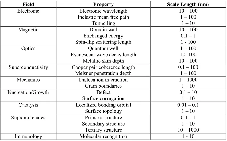
[image:18.612.127.525.430.677.2]Nanotechnology has become the new scientific field as it is found that the smaller the materials were fabricated, they will have unique and interesting physical and chemical characteristic. Nanotechnology have vast and infinity potentiality application such as quantum dot computing, nanopillars as electron emitters for liquid crystal display application and persistent current in nanoring for future energy devices. Scientists have fabricating devices down to atomic precision and the era of fabricating materials at atomic precision were said to be led by Nanotechnology. Table 2.1 shows some of the major research activities at nanoscale regime.
Table 2.1: Characteristic lengths in solid state science model (Murday, 2006).
Field Property Scale Length (nm)
Electronic Electronic wavelength Inelastic mean free path
Tunnelling
10 – 100 1 – 100
1 – 10
Magnetic Domain wall
Exchanged energy Spin-flip scattering length
10 – 100 0.1 – 1 1 - 100
Optics Quantum well
Evanescent wave decay length Metallic skin depth
1 – 100 10- 100 10 – 100 Superconductivity Cooper pair coherence length
Meisner penetration depth
0.1 – 100 1 – 100 Mechanics Dislocation interaction
Grain boundaries
1 – 1000 1 – 10
Nucleation/Growth Defect
Surface corrugation
0.1 – 10 1 – 10 Catalysis Localized bonding orbital
Surface topology
0.01 – 0.1 1 – 10 Supramolecules Primary structure
Secondary structure Tertiary structure
0.1 – 1 1 – 10 10 – 1000
9
At the bulk state, materials show their collected atom’s physical and chemical behaviour and the smaller the sizes of the materials fabricated, their physical and chemical properties will be determined more by the individual atoms such the behaviour of gold that is the main material in this report. At the bulk state, gold is well a known inert, shiny, yellow noble metal that does not tarnish (Hammer & Norskov, 1995) has a face centred cubic (fcc) structure, diamagnetic materials where melts at 1064.18˚C which is physical and chemically will not react with other substances at room temperature.
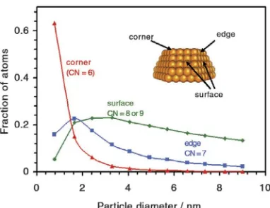
Gold will cease its inert or nobility at nm regime, such as at 3 -5 nm size gold NPs, about few hundred of atoms, they will become an active substances (Haruta et. al, 1997). Gold NPs size less than 2 nm exhibits considerable magnetic properties which turns to ferromagnetic properties (Yamamoto et al., 2006) due to the unpaired electron configuration of their surfaces. Gold NPs about 10 nm sizes will cease its stability of its fcc structure, thus they are arranged in icosahedral, decahedral or defective fcc structures form. By being able to fabricate and control the structure of NPs, scientists and engineers can influence the resulting properties and, ultimately, design materials to give desired properties.
Figure 2.2: Calculated fraction of Au atoms at corners (red), edges (blue) and crystal faces (green) in uniform NPs consisting of the top half of a truncated octahedron as a function of Au particle diameter. The insert shows a truncated octahedron and the
position of representative corner, edges and surface atom (Janssens et al., 2007).
Thin film of gold is an intermediate state between bulk and NPs state where the thickness in the range nanometers to several micrometer. Thin film gold is readily produced on almost any solid substrate either chemical or physical deposition. The example of chemical deposition such as chemical vapor deposition (CVD), electroplating, electroless deposition and so on while the physical deposition include the physical vapor deposition (PVD), pulse laser deposition (PLD) and others. Due to the nobility of gold, such films will generally remain unoxidized, and can be prepared down to a thickness of a few tens of nanometers.
11 2.2 Technique of Fabricating Nanoparticles
Lithography-based techniques are classified according to the tools used and the method of image transfer. These are mainly either direct write type or transfer of a pattern through a photo mask using conventional exposure and development routes. The lithography names varied depends on source of light introduced during the exposure process. For instance, during patterning of masks/ nanoparticles such as using uv light named Photolithography (PL), x-ray as source called X-Ray lithography (XRL), using electron as source of patterning that called Electron Beam Lithography (EBL) and so on. In this discussion, there are several types of patterning technique which will be further discussed in this chapter.
PL technique is a conventional patterning pattern on the substrate by allowing uv light passing through the mask and the patterning appear on the resist either positive resist or negative resist. Pattern which is exposed on the positive resist will become insoluble in developer or organic solvent. However, pattern exposed on the negative resist will become insoluble in the developer and the pattern will become inversed compared to it patterning mask (Jaeger, 2002). PL technique is costly and time consuming due to the series of masking required during the synthesis and the mass production is low.
materials without suffering from considerable distortion effects due to local charge build up (Yao, 2007).
Focused Ion Beam (FIB) technique has same principle as Scanning Electron Microscopy (SEM) or in EBL process; they consist of charged particles that are focused by a series of lenses and aperture onto a sample and employ similar method to produce and accelerate the particles from their source. But in FIB technique, they used bombardment of ion compare to the SEM/EBL which is using electron as source. The FIB have 4 basic function which is milling, deposition, implantation and imaging process. One of the major advantages with FIB compared to an electron beam, especially in patterning nano-magnetic devices, is that the electron beam tends to show physical shifting to an extent of 100 nm due to the interaction between the beam of charged electrons and the magnetic thin film on the substrate to be
patterned, which is almost negligible with an ion beam. Apart from these, the heavier mass of the ions allows direct etch or deposition, thus avoiding the patterning steps used in optical or electron beam (Yao, 2007).
Advances in existing production techniques are improving the quality and yields, providing a clear prospect of commercially viable volume production. World scientists, through investigating of various techniques at nanoscale regime, have shows new trend in nanotechnology research as can be seen in the figure 2.3. The self assemble technique in fabricating nanoparticles have been found to lead others techniques such as Atomic Force Microscopy (AFM) and Scanning Tunnelling Microscopy (STM), since it has these features to offer for future technological advancement.
1. Easy in fabricating nanoparticles. 2. Mass production
3. Versatile in shapes, sizes and materials
13
Figure 2.3: Nanoscience Literature Citation Counts (Murday, 2006)
Simple approaches of growing multidimensional nanostructures by self-assembly phenomena are vapor-liquid-solid (VLS) and vapor-solid (VS) process. VLS process include 2 step processes which is 1) formation of small liquid droplet as catalysts and 2) the alloying, nucleation and growth of nanostructure. However, VS process does not involve the 1st step of VLS process which is liquid droplet as catalysts. In many cases, the growth of 1D nanostructures such as ZnO nanowires were fabricated by decomposing ZnO powder in high temperature assisted by suitable flow gas under atmosphere pressure in the reaction chamber. Both techniques revealed fine nanostructures by controlling temperature, duration time, pressure, size of powder, vapor pressure and etc to vary the length, size and amount of ZnO powder (Fan et al., 2006). In particular, to fulfil the complex requirements and demands of a current nanotechnology, the challenges lie not only in growth themselves but also in the controlling of position makes them arrange in periodic arrays.
film highly ordered, 3D macroporous magnetic networks based on the polystyrene template and the results revealed the higher coercivity and irreversible field than non-templated samples of the same film.
15 2.3. Polystyrene Nanospheres as source of carbon based materials
2.3.1 Type of Nanospheres
[image:25.612.249.402.410.523.2]There are several different materials made of nanospheres such as silica, polystyrene and polymethyl methacrylate (PMMA) beads. Silica or Si2O nanosphere is absolutely made from silica which is semiconductor material. Not many researchers have done experiments using silica nanospheres due to the limitation of modification of chemical and physical properties. One solution of the limitation was introduced (Vossen et al., 2005) where the silica nanospheres were deformed by ion bombardment and expanded in the plane perpendicular to the ion beam. In 2008, Vossen and co-workers have been introduced the chemical modification of silica nanospheres which is more accurate tuning the hole size by controlling amount of tetraethoxysilane (TEOS) added. This method more easy to use, fast and inexpensive compares the previous method. However, PSNs was chosen in our research due to the advantages as describe below.
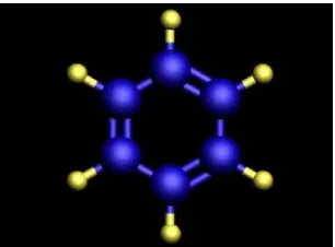
Figure 2.5: Chemical model of benzene ring (Hellrroy, 2008)
shown in Figure 2.5. This orbital allows the electrons to move freely around the ring of carbon atoms (delocalized electrons). Nanotechnologists have demonstrated that molecules such as benzene because they contain these handy delocalized electrons can be used to conduct electrical current in nano-scale electronic devices.
[image:26.612.150.498.402.651.2]We have long accepted that diamond and graphite are different allotropic forms of carbon (Mannion, 2006) which have distinctly different structures, bonding characteristics and therefore grossly different chemical and physical properties. However, graphite (the tip of pencil), also conducts electricity. A graphite molecule is, like benzene, a collection of carbon rings but it’s built differently: The same electrons that benzene uses to bond each carbon atom to a hydrogen atom are used instead to bond carbon atoms to other carbon atoms in adjacent carbon rings. As shown in figure 2.6 (1-c), in this structure, each carbon atom bonds covalently to three other carbon atoms. As with benzene, each carbon atom in graphite has an “extra” electron — one more than the number of atoms it’s bonded to. The atomic orbitals for these electrons overlap to form a molecular orbital that allows delocalized electrons to move freely throughout entire graphite sheet makes graphite conducts electricity.
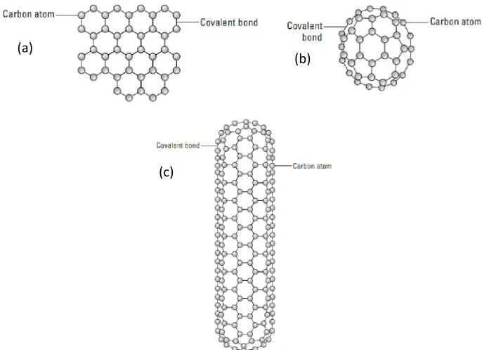
Figure 2.6: Structure of carbon atoms connected by covalent bond in a (a) graphite’s sheet, (b) buckyball and (c) single wall of carbon nanotubes (SWCNTs). (a)
(b)
17 Two properties of carbon group make them especially useful in nanotechnology: their strength and their ability to conduct electricity. Buckyballs and single wall carbon nanotubes (SWCNTs) are two types of simplest molecules composed of carbon atoms that have wide applications in nanotechnology such in electronics, biology, chemistry, medical, mechanical and etc (Harris, 2009). The simplest structure of buckyballs contain 60 carbon atoms form a single stable molecule only if they are arranged in 20 hexagons and 12 pentagons that are linked to form a sphere (Mitin et al., 2008) about 1 nm diameter.
Like bulkyballs, SWCNTs are combination of carbon atom instead of forming the shape of a sphere, the lattice forms the shape of a cylinder as illustrated on figure 2.4(c) which conduct electricity better than metals. When electrons travel through metal there is some resistance to their movement. This resistance happens when electrons bump into metal atoms. When an electron travels through a SWCNT, it’s travelling under the rules of quantum mechanicals with low or without scattering event thus travel in maximum mobility of bulk materials. Therefore the movement of electron in SWCNT called ballistic transport (O’Connell, 2006).
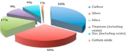
[image:27.612.219.435.577.664.2]Why is carbon material very important? This is due to the carbon materials relate to the chemistry, physics and biology of this versatile element described previously. Chemically, carbon is highly reactive and can be combined with many other elements to produce a wide variety of compound, either simple or complex compound (Jones, 2001). Nevertheless, carbon is very important in terms application because it has industrial and social uses and so are component of wealth generation. Figure 2.7 shows a summary of nanomaterials used in consumer as product. Carbon was selected as the most demanded by consumers as it is inexpensive materials and the ability to bond or easily join, some of the reasons why carbon include carbon compounds are common in our universe (Saucerman, 2005).
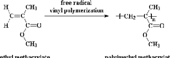
Nevertheless polymethyl methacrylate (PMMA) is a type of polymer, it can be fabricated in sphere shape or in liquid matter. PMMA does not have benzene ring in chemical structure as shown in figure 2.8 and to a certain extent, researchers not give much attention in modification of physical and chemical structures of PMMA nanospheres. For instance, magnetic hollow of PMMA nanospheres were successfully developed via in situ emulsion polymerization in the presence of oleic acid-modified Fe3O4@CaCo3 composite NPs and obtain the magnetic hollow by etching the CoCO3 as templates. Fe3O4 was proved to be existed in the hollow of PMMA nanosphere which endowed the PMMA nanospheres with magnetic properties. The magnetic properties have been shown by PMMA nanospheres could be applied in various fields of controlled release, drug delivery, target delivery and so on (Chunlei et al., 2010).
Figure 2.8: Model of polymerization of methyl methacrylate.
2.3.2 A flexible technology of polymer electronics
Polymer can be defined as the large chain of repeating structural unit called monomer. Polymers can be classified as natural if they made from nature such as rubber or protein and synthetic if they are human made such as polystyrene. In semiconductor industry, polymer as PMMA used as the polymer resist either positive or negative as previously described.
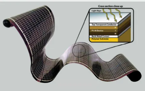
19 solar cells (Pagliaro, 2008) which the polymer used as the substrate in a sandwich layer of solar panel as shown in figure 2.9.
Figure 2.9: Flexible solar panels used polymer as substrate (Pagliaro, 2008).
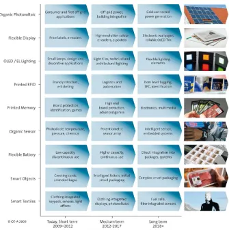
Figure 2.10: Third Organic Electronic Association (OE-A) Roadmap describes future focus of the industry (Hecker, 2009).
[image:30.612.191.460.492.643.2]21 In practise, the photoactive organic layer is placed between two different electrodes, the upper being transparent (figure 2.12 (a) and (b)). Charge separation takes place in the organic phase, the anode and cathode being chosen to have largely different (asymmetric) work functions, and thus to enhance modest charge separation. In photovoltaic (PV), light is absorbed mainly in the so-called donor material, a hole-conducting small molecule or conjucted polymer. The photogenerated singlet excitons diffuse within the donor towards the interface to the second material, the acceptor, which is usually strongly electronegative for example C60. However, mechanism in light emitting diode (LED) is opposite mechanism in PV by releasing light as shown in figure (a).
Figure 2.12: Organic materials sandwiched between two electrodes can work as (a) LED or (b) PV devices. In the former case electrons are collected at the metal electrode and holes at the iodium-tin oxide (ITO) electrode (Spanggaard & Krebs,
2004).
2.4 Nanosphere Lithography Technique
NSL also has other names: natural lithography (Deckman et al., 1982), colloidal lithography (Yang, et al., 2006), shadow nanosphere lithography (Kosiorek et al., 2005) and nanosphere photolithography (Wei, 2007). In 1981, Fischer and Zingsheim reported the use of a simple drop-coated, colloidal monolayer with diameter of 312 nm onto a glass plate as a lithographic mask for preparation of platinum (Pt) nanostructures. The size and the periodicity of the Pt patterns were smaller than the visible light (Fischer et al., 1981). However, the focus of this work was on replication of submicroscopic patterns using visible light and not realization of lithographic colloidal masks.
One year later, Deckman and Dunsmuir have extended the idea of this technique. They have shown results of two-fold mask preparation: using
electrostatic adsorption and the spinning coating technique. Because the mask preparation process was based on the naturally occurring self-assembly phenomenon, they named this strategy as “Natural Lithography” (Deckman et al., 1982).Over the last ten years Van Duyne et al. have popularized natural lithography under the name of “nanosphere lithography” (Haynes et al., 1995). Since the pioneering works of Fischer et al. and Deckman et al., many groups have started to develop new approaches and to improve established methods in order to fabricate better quality colloidal masks and more sophisticated nanostructures depending on application.
2.4.1 Modification of polystyrene nanospheres (PSNs)
Thermal energy is a simplest way or source of energy in modification of PSNs whether using oven, hot plate or microwave treatment. Fe2O3 and silica hexagonal periodic triangular prism nanopillars were successful fabricated by heat-induced deformation of PSNs using oven. Unheated PSNs will result truncated-hollow sphere Fe2O3 due to position of PSNs in close-packed lattice structures and contact with each other by quasi style in monolayer. However heating PSNs makes the contact of PSNs change from quasi point contact to facet contact resulting triangular prism nanopillars. Interestingly, the morphologies are different from those obtained by the templates with heating and without heating. However, over-heating PSNs will make the channel between PSNs will disappear, therefore no nanopillars were fabricated (Li et al., 2005).
23 the inefficiency of selectivity heating by hot plates. Additionally, no wirelike structures are formed because the arching of metal is inefficient. By employing the conventional heating source to anneal Au-polystyrene beads substrate is not effective in modifying the morphology of metals because high annealing temperature leads to the serve deformation of PSNs. Well-controlled postgrowth microwave treatment on the Au-PSNSs for effectively improving the SERS performance. This method enables the selective modification and discharging of Au films while minimizing the thermal effect on PSNs, thereby promoting greatly enhanced SERS activities (Clement et al., 2008).
The changes of physical properties of PSNs have been investigated by Agam and Guo (2007) by radiating the PSNs to the electron radiation under room temperature. The shrinkage of PSNs offers a new route in modification of NSL technique where the diameter of PSNs linearly decreased by increasing the duration time exposed. The shrinkage is likely to be caused by electron-induced damage of the polymer chain, resulting in partial loss of hydrogen and the formation of amorphous carbon like structures (Agam et al., 2007).
Wu and colleagues (2008) developed a maskless PL named nanosphere photolithography (NSPL) utilizing the silica micro-sphere (1 µm) to focus uv light for fabricating periodic metallic nanoholes perforated in gold and aluminium films. Silica micro-spheres were spun on a standard commercial positive and negative photoresist before exposing UV light. Metal layers of Au were deposited by electron-beam evaporator. After development, the positive resist will result in gold nanopost whereas the negative resist will result in gold nanoholes. The diameters of Au nanoholes and nanoposts about 180 nm. The simulation results show that even smaller nanoholes with tunable periods can be generated with a shorter wavelength.
2.4.2 NSL as versatile technique to produce periodic Nanoparticle Arrays (PNPAs).
Nanotriangles is a basic shape of nanostructure arrays fabricated using PSNs as templates by deposition of metal using metal deposition evaporator, electron-beam evaporator and etc., filled the voids between the arrangements of PSNs in hexagonal closed pack. Deckman et al. (1982) evaporated silver over hexagonal closed pack arrays of 0.4 µm PSNs and the nanotriangles left on the substrate after dissolved in methylene chloride. Haes et al (2005) have extended the basic shape of nanotriangles by releasing them in solution rather than on the substrate. They discovered that the nanoparticles are weakly attracted to the glass surface, therefore they take these advantages to released the nanotriangles and become suspended in the solution, which is ethanol. Later, they investigate the Localized Surface Plasmon Resonance (LSPR) spectrum of the nanotriangles suspended in the bulk ethanol and reported that there are two maximum peaks LPSR spectrums at 417.9 and 682.1 nm compared to nanotriangles on substrate that has only an extinction maximum at 645.6 nm. Later they tried to simulate the experimental results as they are interested to understand why nanoparticles in suspension solution showed two peaks at LPSR spectrum.
They started with Mia theory to model the LPSR spectrum of suspended nanoparticles in solution. They started with hexadecanethiol-coated Ag nanosphere with radius ranging from 5, 10, 15 and 20 nm. As the size of sphere radius increases the LSPR extinction maximum increase from ~390 nm to 410 nm. The model are further investigated using Discrete Dipole Approximation (DDA) to model the nanoparticles with different sizes and shapes, where the nanotriangles nanoparticles were represented as cubic lattice to formed as polarized points. From both theoretical results, the intense local maximum centered at ~ 420 nm (experimental) arises from the combined effect from the absorption of small spherical nanoparticles and the out-of-plane polarization of truncated tetrahedral nanoparticles are better explained (Haes et al., 2005).
67
REFERENCES
Agam, M. A. (2006). An Investigation of Physical Processes in Nanosphere Lithography. University of Birmingham: Ph.D. Thesis.
Agam, M. A. and Guo, Q. (2007). Electron Beam Modification of Polymer Nanospheres. Journal of Nanoscience and Nanotechnology, 7(10), pp. 1 – 5.
Amanda, J. H., Christy, L. H. and Richard, P. V. D. (2001). Nanosphere Lithography: Self-Assembled Photonic and Magnetic Materials. Mat. Res. Soc. Symp., 636.
Barbalace, K. (2007). Periodic Table of Elements - Sorted by Electronegativity
(Pauling). Retrieved March 03, 2012, from
http://EnvironmentalChemistry.com/yogi/periodic/electronegativity.html
Bartlett, P. N.,Ghanem, M. A., El Hallag, I. S., Groot, P. D. & Zhukov, A. (2003). Electrochemical Deposition of Macroporous Magnetic Networks Using Colloidal Templates. J. Mater. Chem., 13, pp. 2596–2602.
Basford, L. (1968). Electricity. Britain: Willam Heinemann Ltd. pp. 73 - 75.
Bechelany, M., Brodard, P., Philippe, L. and Michler, J. (2009). Extended Domains of Organized Nanorings of Silver Grains as Surface-Enhanced Raman Scattering Sensors for Molecular Detection. Nanotechnology, 20.
Blaber, M. G., Ford, M. J. & Cortie, M. B. (2009). Gold Science and Application. United States of America: CRC Press, pp. 21.
Bratlie, K. M., Lee, H., Komvopoulos, K., Yang, P. & Somorjai, G. A. (2007) Platinum Nanoparticle Shape Effects on Benzene Hydrogenation Selectivity. Nano Letters, 7(10), pp. 3097 – 3101.
Burgers, A. R., Bultman, J. H., Beneking, C., Nositschka, W. A., Voigt, O. and Kurz, H. (2000). Silicon Solar Cells Textured by Reactive Ion Etching with Natural Lithography. 16th European Photovoltaic Solar Energy Conference, pp. 1 – 4.
Byrne, D., Schilling, A., Scott, J. F. & Gregg, J. M. (2008). Ordered Arrays of Lead Zirconium Titanate Nanorings. Nanotechnology, 19(16), pp. 1 – 5.
Chen, H. L., Chuang, S. Y., Lin, C. H. and Lin, Y. H. (2007). Using Colloidal Lithography to Fabricate and Optimize Sub-Wavelength Pyramidal and Honeycomb Structures in Solar Cells. Optics Express, 15(22).
Cheung, C. L., Nikolic, R. J., Reinhardt, C. E. and Wang, T. F. (2006), Fabrication of Nanopillars by Nanosphere Lithography. Nanotechnology, 17(5), pp. 1339 – 1343.
Chunlei, W., Juntao, Y., Xuejun, C., Dengli, C. & Hongyan, W. (2010). Preparation and Characterization of Magnetic Hollow PMMA Nanospheres via in Situ Emulsion Polymerization. Colloids and Surfaces A: Physicochem. Eng. Aspects , 363(1-3), pp. 71-77.
Clark, J. (2011). How the heterogeneous catalyst works (in general terms). Retrieved
February 28, 2012, from
69 Clement, Y., Wei, Z. & Zhiwei, H. (2008). Improving Surface-Enhanced Raman Scattering Effect Using Gold-Coated Hierarchical Polystyrene Bead Substrate Modified with Postgrowth Microwave Treatment. Journal of Biomedical Optics, 13(6).
De Rogatis, L., Cargnello, M., Gombac, V., Lorenzut, B., Montini, T., Fornasiero, P. (2010). Embedded Phases: A Way to Active and Stable Catalysts. ChemSusChem. 3(1), pp. 24 – 42.
Deckman, H. W. & Dunsmuir, J. H. (1982). Natural Lithography. Appl. Phys. Lett. 41(4), pp. 377.
Dendukuri, D., Gu, S. S., Pregibon, D. C., Hatton, T. A. & Doyle, P. S. (2007). Stop-flow Lithography in a Microfluidic Device. Lab. Chip, 7(7), pp. 818 – 828.
Fan, H. J., Werner, P. & Zacharias, M. (2006). Semiconductor Nanowires: from Self-Organization to Patterned Growth. Small, 2(6), pp. 700-717.
Fengqiang, S., Weiping, C., Yue, L., Lichao, J. and Fang, L. (2005). Direct Growth of Mono- and Multilayer Nanostructured Porous Films on Curved Surface and Their Application as Gas Sensors. Adv. Mater., 17(23), pp. 2872 – 2877.
Fischer, U. C. & Zingsheim, H. P. (1981). Submicroscopic Pattern Replication with Visible Light. J. Vac. Sci. Technol., 19, pp. 881-885.
Flint, D. (2011). Why Are Transition Metals Good Catalysts? Retrieved: March 6, 2012 at http://www.ehow.com/about_6686789_transition-metals-good-catalysts_.html.
Frey, L., Lehreer, C. and Ryssel, H. (2003). Nanoscale Effects in Focused Ion Beam Processing. Applied Physics A Materials Science Processing, 76(7), pp. 1017 – 1023.
Fuhrmann, B., Leipner, H. S. & Hoche, H. –R. (2005). Ordered Arrays of Silicon Nanowires Produced by Nanosphere Lithography and Molecular Beam Epitaxy. Nano letters, 5(12), pp. 2524 – 2527.
Groenendaal, L. B., Jonas, F., Freitag, D., Peilartzik, H. & Reynolds, J. R. (2000). Poly(3,4-ethylenedioxythiophene) and its Derivatives: Past, Present, and Future. Advanced Materials, 12(7), pp. 481 – 494.
Haes, A. J., Jing, Z., Shengli, Z., Own, C. S., Marks, L. D., Schatz, G. C. & Duyne, R. P. V. (2005). Solution-Phase, Triangular Ag Nanotriangles Fabricated by Nanosphere Lithography. Journal of Physical Chemistry B, 109(22), pp. 11158-11162.
Hammer, B. & Norskov, J. K. (1995) Why Gold is the Noblest of All the Metals. Nature, 376(6537), pp. 238 – 240.
Hansen, G. W. (2007). Fundamentals of Nanoelectronics. Upper Saddle River, NJ : Prentice Hall, pp. 321 – 323.
Harris, P. J. F. (2009). Carbon Nanotube Science: Synthesis, Properties and Applications. Cambridge: Cambridge University Press. pp. 146 -220.
Haruta, M. (1997). Size and Support Dependency in the Catalysts of Gold. Catalysis Today, 36(1), 153 – 166.
71 Hecker, K. (2009). Third OE-A Roadmap Describes Future Focus of the Industry.
Retrieved March 7, 2011, from p. 1 at
http://www.nanowerk.com/news/newsid=11383.php
Holiday, R. & Corti, C. (2009). Miscellaneous Uses of Gold. in Gold: Science and Application. United States of America: CRC Press, pp. 400.
Huang, Y. –W., Wu, C. –H. & Aronstam, R. S. (2010). Toxicity of Transition Metal Oxide Nanoparticles: Recent Insights from in vitro Studies. Materials, 3(10), pp. 4842 – 4859.
Hulteen, J. C. & Duyne, R. P. V. (1995). Nanosphere Lithography: A Materials General Fabrication Process for Periodic Particle Array Surfaces. J. Vac. Sci. Technol. A 13(3), pp. 1553.
Jaeger, R. C. (2002). Introduction to Microelectronic Fabrication. United States of America: Prentice Hall, pp. 24.
Jang, S. G., Choi, D. –G., Heo, C. –J., Lee, S. Y. & Yang, S. -M. (2008). Nanoscopic Ordered Voids and Metal Caps by Controlled Trapping of Colloidal Particles at Polymeric Film Surfaces. Advanced Materials, 20(24), pp. 4862 – 4867.
Jang, S. G., Yu, H. K., Choi, D. –G. & Yang, S. –M. (2006). Controlled Fabrication of Hollow Metal Pillar Arrays Using Colloidal Masks. Chemistry of Materials, 18(26), pp. 6103 – 6105.
Janssens, T. V. W., Clausen, B. S., Hvolbaek, B., Falsig, H., Christensen, C. H., bligaard, T. & Norskov, J. K. (2007). Insights into the Reactivity of Support Au Nanoparticles: Combining Theory and Experiments. Topics in Catalysis, 44(1-2), pp. 15-26.
Jeong, G. H. Park, J. K., Lee, K. K., Jang, J. H., Lee, C. H., Kang, H. B. and Suh, S. J. (2010). Fabrication of Low-Cost Mold and Nanoimprint Lithography Using Polystyrene Nanosphere. Microelectronic engineering, 87(1), pp. 51 – 55.
Johnson, B. F. G. (2003). Nanoparticles in Catalysis. Topics in Catalysis, 24(1 – 4), pp. 147 – 159.
Jones, C. J. (2001). D- and f-Block. UK: Royal Society of Chemistry, pp. 57-59.
Kevan, S. D. (1990). Surface Fermi Surfaces. Phys. Scr. Vol. T31, pp. 32-34,
Kosiorek, A., Kandulski, W., Glaczynska, H. & Giersig, M. (2005). Fabrication of Nanoscale Rings, Dots and Rods by Combining Shadow Nanosphere Lithography and Annealed Polystyrene Nanosphere Masks. Small, 1(4), pp. 439 – 444.
Kulesza, P. J., Marassi, R., Karnicka, K., Wlodarczyk, R., Miecznikowski, K., Skunik, M., Kowalewska, B., Chojak, M., Baranowska, B., -Zurowska, A. K. & Ginalska, G. (2007). Electrocatalysis and Bioelectrocatalysis at Nanostructured Composite Films. Rev. Adv. Mater. Sci., 15, pp. 225 – 233.
Kulesza, P. J., Marassi, R., Karnicka, K., Wlodarczyk, R., Miecznikowski, K., Pagliaro, M., Ciriminna, R., & Palmisano, G. (2008). Flexible Solar Cells. Chem. SusChem, 1(11), pp. 880 -891.
Kuo, C., -W., Shiu, J. –Y., Cho, Y. –H. & Chen, P. (2003). Fabrication of Large-Area Periodic Nanopillar Arrays for Nanoimprint Lithography Using Polymer Colloidal Masks. Advanced Materials, 15(13), pp. 1065 – 1068.
73 Oxygen Reduction Catalyst. Abs. 321, 205th Meeting, The Electrochemical Society, Inc.
Li, C., Hong, G., Wang, P., Yu, D. & Qi, L. (2009). Wet Chemical Approaches to Patterned Arrays of Well-Aligned ZnO Nanopillars Assisted by Monolayer Colloidal Crystals, Chem. Mater., 21(5), pp. 891–897.
Li, Y., Cai, W., Cao, B., Duan, G. & Sun, F. (2005). Fabrication of the Periodic Nanopillar Arrays by Heat-Induced Deformation of 2D Polymer Colloidal Monolayer, Polymer, 46, pp. 12033 – 12036.
Ling, X., Wei, L., Jun, X., Jiang, Z., Liangcai, W., Xian-Gao, Z., Zhongyuan, M. & Kunji, C. (2009). Morphology Control and Electron Field Emission Properties of High-Ordered Si Nanoarrays Fabricated by Modified Nanosphere Lithography. Applied Surface Science, 255(10), pp. 5414–5417.
Liu, Y., Kim, E., Ghodssi, R., Rubloff, G. W., Culver, J. N., Brntley, W. E. & Payne, G. F. (2010). Biofabrication to Build the Biology-Device Interface. Biofabrication, 2(2).
Lu, Z. –C., Ruan, W. –D., Ren, L. –Q., Cong, Q. and Zhao, B. (2006). Fabrication of Large-Scale Nanostructure by Langmuir-Blodgett Technique. Journal of Bionic Engineering, 3(2), pp. 59 – 62.
Ma, Y., Wong, C. P., Zeng, X. T., Yu, T., Zhu, Y. and Shen, Z. X. (2009). Pulsed Laser Deposition Of ZnO Honeycomb Structures on Metal Catalysts Prepatterned Si Substrate. Journal of Physics D: Applied Physics, 42(6), pp. 1 – 6.
Marikani, A. (2009). Engineering Physics. New Delhi: PHI Learning Private Limited. pp. 230.
Masahide, T., Koji. U., Takahiro, M., Jianxi, Y., Yomei, T., Toshinobu, Y., Stefano, C., Luca, M. and Plinio, I. (2008). Bottom-up and Top-Down Approach for Periodic Microstructures on Thin Films by Controlled Photo-Activated Chemical Processes. J. Sol.-Gel Sci Technol 48, pp. 182 – 186.
Minges, M. L. (1989). Electronic Materials Handbook. ASM International, pp. 96.
Mitin, V. V., Kochelap, V. A & Stroscio, M. A. (2008). Introduction to Nanoelectronics: Science, Nanotechnology, Engineering and Applications.
Cambridge: Cambridge University Press, pp. 102 -103.
Moon, J. H., Jang, S. G., Lim, J. –M. & Yang, S. –M. (2005). Multiscale Nanopatterns Templated from Two-Dimensional Assemblies of Photoresist Particles. Advanced Materials, 17(21), pp. 2559 – 2562.
Moon, J. H., Yang, S. –M, Pine, D. J. & Chang, W. -S. (2004). Multiple-Exposure Halographic Lithography with Phase Shift. Applied Physics Letters, 85(18).
Murday, J. S. (2006). The Coming Revolution Science and Technology of Nanoscale Structures. The AMPTIAC Newsletter, 6(1), pp. 5 – 10.
Nakae, Y.,Seino, Y., Teranishi, T., Miyake, M., Yamada, S. & Hori, H. (2000) Anomalous Spin Polarization in Pd and Au Nano-Particles. Physica B, 284-288(Part 2), pp. 1758 – 1759.
Nave, R. (2002). Fermi Level. Retrieved March, 6, 2012 at http://hyperphysics.phy-astr.gsu.edu/hbase/solids/Fermi.html
75 Nur, H., Hayati, F. & Hamdan, H. (2007). On the location of deferent titanium sites in Ti–OMS-2 and their catalytic role in oxidation of styrene. Catalysis Communications, 8, pp. 2007–2011.
O’ Connell, M. J. (2006). Carbon Nanotubes: Properties and Applications. Boca Raton, FL: Taylor & Francis Group, pp. 85.
Overbury, S. H., Ortiz-Soto, L., Zhu, H., Lee, B., Amiridis, M. D. & Dai, S. (2004) Comparison of Au Catalysts Supported On Mesoporous Titania and Silica: Investigation of Au Particle Size Effects and Metal-Support Interactions. Catalysis Letters, 95(3-4), pp. 99 – 106.
Park, K. H., Lee, S., Koh, K. H., Lacerda, R., Teo, K. B. K. & Milne, W. I. (2005). Advanced Nanosphere Lithography for the Real-Density Variation of Periodic Arrays of Vertically Aligned Carbon Nanofibers. Journal of Applied Physics, 97(2).
Peacock, A. & Calhoun, A. (2006). Polymer Chemistry: Properties and Application. Munich: Hanser Publishers, pp. 309.
Ramaswamy, A. V. (2009). Homogeneous Catalysis and Fine Chemicals. in Viswanathan, B. Catalysis: Selected Application. Oxford: Alpha Science, 6.2
Roduner, E. (2006). Nanoscopic Materials: Size –Dependent Phenomena. Dorset: RCS Publishing, pp. 7.
Roduner, E. (2006). Size Matters: Why Nanomaterials are Different. Chem. Soc. Rev., 2006, 35(7), pp. 583 – 592.
Saucerman, L. (2005).Understanding the Element of the Periodic Table: Carbon. New York: Rosen Publication Group, pp 10.
Shishoo, R. (1996). Plasma Treatment – Industrial Application and Its Impact on the C&L Industry. Journal of Coated Fabrics, 26, pp. 26-35.
Spanggaard, H. & Krebs, F. C. (2004). A Brief History of the Development of Organic and Polymeric Photovoltaics. Solar Energy Materials & Solar Cells 83(2 – 3), pp. 125–146.
Su, H., Li, Y., Li, X. –Y. & Wong, K. S. (2009). Optical and Electrical Properties of Au Nanoparticles in Two-Dimensional Networks: An Effective Cluster Model. Optics Express, 17(24), pp. 22223 – 22234.
Subramaniam, A. B., Lecuyer, S., Ramamuthi, S., Losick, R. & Stone, H. A. (2010). Particle/Fluid Interface Replication as a Means of Producing Topographically Patterned Polydimethylsiloxane Surfaces for Deposition of Lipid Bilayers. Adv. Mater., 22(19), pp. 2142 – 2147.
Tao, A. R., Habas, S. & Peidong Y. (2008). Shape Control of Colloidal Metal Nanocrystals, Small, 4(3), pp. 310 – 325.
Tomasino, C., Cuomo, J.J., and Smith, C.B. (1995). Plasma Treatments of Textile. Journal of Coated Fabrics, 25, pp. 115-127.
Tripathi, P. K. (2012). Computer Interface to Accurately Determine Fermi Energy and Fermi Temperature of Materials. International Journal of Computer Applications, 38(2), pp. 44 – 49.
77 Ulgut, B & Suzer, S. (2003). XPS Studies of SiO2/Si System under External Bias. J.
Phys. Chem. B, 107(13), pp. 2939 – 2943.
Vossen, D. L. J., Fific, D., Penninkhof, J., Dillen, T. V., Polman, A. & Blaaderen, A. V. (2005). Combined optical Tweezers/Ion Beam Technique to Tune Colloidal Masks for Nanolithography. Nano Letters, 5(6), pp. 1175 – 1179.
Vossen, D. L. J., Penninkhof, J. J. & Blaadered, A. V. (2008). Chemical Modification of Colloidal Masks for Nanolithography. Langmuir, 24(11), pp. 5967 – 5969.
Wu, W., Dey, D., Memis, O. G., Katsnelson, A. & Mohseni, H. (2008). Fabrication of Large Area Periodic Nanostructures Using Nanosphere Photolithography. Nanoscale Res Lett, 3(10), pp. 351 – 354
Wu, W., Dey, D., Memis, O. G., Katsnelson, A. & Mohseni, H. (2008). A Novel Self-Aligned and Maskless Process for Formation of Highly Uniform Arrays of Nanoholes and Nanopillars. Nanoscale Research Letters, 3(3), pp. 123 – 127.
Wisitsoraat, A., Mongpraneet, S., Phatthanakun, R., Chomnawang, N., Phokharatkul, D., Patthanasettakul, V. & Tuantranont, A. (2010). Low-Cost and High-Resolution X-Ray Lithography Utilizing a Lift-Off Sputtered Lead Film Mask on a Mylar Substrate. J. Micromech. Microeng. 20, pp. 1 – 7.
Wood, M. A. (2007). Colloidal Lithography and Current Fabrication Techniques Producing in-Plane Nanotopography for Biological Applications. J. R. Soc. Interface, 4(12), pp. 1 – 17.
Yang, S. -M., Jang, S. G., Choi, D. -G., Kim, S. & Yu, H. K. (2006). Nanomachining by Colloidal Lithography. Small, 2(4), pp. 458-475.
Yao, N. (2007). Focused Ion beam Systems: Basics and Applications. Cambridge: Cambridge University Press, pp. 2-3.
Zeghbroeck, B. V. (2007). Semiconductor Fundamentals. Retrieved March 7, 2011, from http://ecee.colorado.edu/~bart/book/book/chapter2/ch2_3.htm#2_3_3
Zhang, Y. J., Li, W. and Chen, K. J. (2008). Application of Two-Dimensional Polystyrene Arrays in the Fabrication of Ordered Silicon Pillars. Journal of Alloys and Compounds, 450(1 – 2), pp. 512 – 516.
Zhou, B., Balee, R., Groenendaal, R. (2005). Nanoparticle and Nanostructure Catalysts: Technologies and Markets. Nanotechnology Law & Business, 2(3), pp. 222 – 229.
Zhou, X., Liu, K. Y., Knoll, W., Quan, C. & Zhang, N. (2010). 3D Profile Simulation of Metal Nanostructures Obtained by Closely Packed Nanosphere Lithography. Plasmonics, 5(2), pp. 141-148.
Zhou, X., Zhang, N., Liu, K. Y., Tan, C. & Knoll, W. (2009). Dispersion of Nanospheres on Large Glass Substrate by Amorphous or Polycrystalline Silicon Deposition for Localized Surface Plasmon Resonance. Journal of Nanoparticle Research, 11(8), pp. 2061 – 2069.
Zinola, C. F. (2010). Electrocatalysis: Computational, Experimental, and Industrial Aspects. Boca Raton: Taylor & Francis, pp. 43.