2017 International Conference on Computer, Electronics and Communication Engineering (CECE 2017) ISBN: 978-1-60595-476-9
Micromorphology of AlN Epilayers on Sapphire Substrates
Ştefan
ŢĂLU
1,*, Dinara SOBOLA
2, Pavel TOMÁNEK
2and Sebastian STACH
31Technical University of Cluj-Napoca, Faculty of Mechanical Engineering, Department of AET, Discipline of Descriptive Geometry and Engineering Graphics, 103-105 B-dul Muncii St.,
Cluj-Napoca 400641, Cluj, Romania
2Brno University of Technology, Faculty of Electrical Engineering and Communication, Physics Department, Technická 8, 616 00 Brno, Czech Republic
3University of Silesia, Faculty of Computer Science and Materials Science, Institute of Informatics, Department of Biomedical Computer Systems, ul. Będzińska 39, 41-205 Sosnowiec, Poland
*Corresponding author
Keywords: Aluminum nitride, Atomic force microscopy, Fractal analysis, Minkowsky functionals, Surface micromorphology.
Abstract. The purpose of this paper was to describe the 3D nano-scaled surface topography of the aluminum nitride on sapphire. The structures were prepared by magnetron sputtering with heating of the sapphire substrate. The dependence of the layers topography on the substrate temperature was presented. Surface appearance was studied by atomic force microscopy (AFM). The quantitative topography data from AFM were used for surface characterization by fractal analysis and statistical parameters. The results of fractal analysis show the correlation of fractal dimension and statistical characteristics of surface topography. The data may contribute to manufacture of AlN thin films with desired surface characteristics.
Introduction
The sizes of the electronic components decreases and causes study of advanced materials for electronics. Especially this is of great interest for power electronics, where components have to carry out heavy-duty applications. Market of power devices requires further application of prospective semiconductor materials. The choice of wide band gap semiconductors such as AlN for power electronics is obvious due to stability to extreme conditions of exploitation, to localization of electric and magnetic fields, local heating etc. [1, 2].
Aluminum nitride (AlN) is interesting for electronic engineering as a wide band gap semiconductor (6,2 eV) because the band gap can be changed in wide rage by using dopants. It provides and lot of possibilities for design of power electronics. The value of band gap also determines high intensity of electric field for a break down [1]. Structures on the basis of AlN are wide used for application at high temperatures.
AlN material could be found in electronics in different forms: powder, ceramic, layers in heterostructures, substrates. Nowadays there is a significant trend to decrease the size of devices. It means that choice of the materials depends both on the sizes of the semiconductor structures and their suitable physical properties and stability. Preparation of thin AlN layers contributes to the field of materials for power electronics. Since it hasn’t own substrates, fabrication of the AlN layers is a challenging task. There are different methods for preparation of the structures (atomic layer deposition, molecular beam epitaxy, magnetron sputtering, etc.) and every method has a number of parameters that influence the process and quality of the prepared semiconductor films. Here we study the influence of substrate temperature on the topography of the AlN film [1-3].
Materials and Methods
Magnetron sputtering was used for preparation of the AlN films. For the target material aluminum target was used. Nitrogen component was compensated from HF-activated plasma. The sapphire substrates were processed and then used for the films deposition. The experiment was carried out three times for different temperature of the substrate: 1000 K, 1300 K and 1500 K. The temperature of the sputtering process components plays a significant role for the result structures. The structural quality and composition were presented in studies [1].
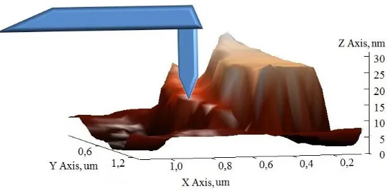
[image:2.612.239.522.284.423.2]AFM was used for study of the surface appearance. It is widely used for estimation of components quality in electronic engineering. AFM provides information about the surface in air without any special procedures of samples preparation. The real 3D topography parameters could be obtained after routine and careful calibration of the device. The obtained data could be presented as matrix of numbers: matrix has the size of the scan, where every number is a high of the sample at XY coordinates (Figure 1).
Figure 1. Scanning of the surface by AFM probe.
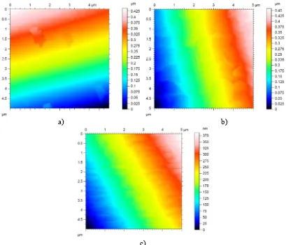
Results and Discussion
a) b)
[image:3.612.102.511.64.415.2]c)
Figure 2. A representative AFM image of AlN nanolayer on the sapphire substrate obtained, for scanning square areas of 5 × 5 m2, at: a) 1000 K, b) 1300 K, c) 1500 K.
Fractal Analysis of Surface Roughness
In our study the fractal geometry was used to characterize complex 3-D irregular patterns and surface structures [1, 3]. It is known that a fractal 3-D engineering surface exhibits topographical features that are independent of the measurement scale and is characterized by a spatial scale-invariance [3]. The fractal dimension D (a non-integer value within the range 2 ≤ D ≤ 3) is a quantitative parameter to globally estimate the 3-D fractal surface complexity [1, 3].
In this study, the fractal analysis was applied to the original AFM files using the cube counting method (derived directly from a definition of box-counting fractal dimension) with a linear interpolation type (the interpolated value in a point is calculated from the three vertices of the Delaunay triangulation triangle containing the point), which is described in detail in Ref. [4].
The fractal dimension of the surface samples, computed according the Ref. [4] is shown in Table 1. The average Df results were expressed as mean value and standard deviation.
Table 1. The fractal dimensions Df values, for scanning square areas of 5 × 5 m2, for AlN nanolayer
on the sapphire substrate obtained at: a) 1000 K, b) 1300 K and c) 1500 K.
The fractal dimensions Df of the surface samples
Samples at temperature 1000 K
Samples at temperature 1300 K
Samples at temperature 1500 K Df 2.29 ± 0.0001 2.42 ± 0.0001 2.66 ± 0.0001
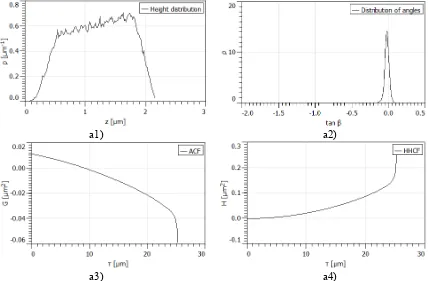
a1) a2)
[image:4.612.97.521.66.343.2]
a3) a4)
Figure 3. The height, the slope distribution function, the autocorrelation function (ACF), and the height-height correlation function (HHCF) for sample from Figure 2a (where p is the corresponding quantity, height or slope; and abscissa is the
tangent of the angle), computed as non-cumulative: a) 1000 K.
a1) a2)
a3) a4)
Figure 4. The height, the slope distribution function, the autocorrelation function (ACF), and the height-height correlation function (HHCF) for sample from Figure 2b (where p is the corresponding quantity, height or slope; and abscissa is the
[image:4.612.93.521.390.671.2]
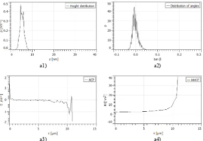
a1) a2)
[image:5.612.101.516.65.354.2]
a3) a4)
Figure 5. The height, the slope distribution function, the autocorrelation function (ACF), and the height-height correlation function (HHCF) for sample from Figure 2c (where p is the corresponding quantity, height or slope; and abscissa is the
tangent of the angle), computed as non-cumulative: a) 1500 K.
Summary
The AlN nanolayers on the sapphire substrate surface of all samples appeared relatively smooth, with very fine nano-asperities spread on the surface due to the preparation processes. Our results suggest that the AlN thin film surface morphology gets better with the increase in temperature of Al2O3
substrate and can be tailored to feature unusual properties. We have also demonstrated that the AlN thin films are fractal in nature.
The nano-topography of the AlN nanolayers on the sapphire substrate can open a new perspective and allow new interesting research on electro-physical, mechanical, and thermal properties, for the future expansion, both in breadth and depth. The fractal analysis in correlation with the AFM data information provides a greater insight into surface roughness quality control and performance of AlN thin films.
Acknowledgement
Research described in the paper was financially supported by the Ministry of Education, Youth and Sports of the Czech Republic under the project CEITEC 2020 (LQ1601), by project Sensor, Information and Communication Systems SIX CZ.1.05/2.1.00/03.0072 and by the Grant Agency of the Czech Republic under no. GACR 15-05259S.
References
[2] Ş. Ţălu, Micro and nanoscale characterization of three dimensional surfaces. Basics and applications. Napoca Star Publishing House, Cluj-Napoca, Romania, 2015.
[3] S. Stach, D. Dallaeva, Ş. Ţălu, P. Kaspar, P. Tománek, S. Giovanzana, L. Grmela, Morphological features in aluminum nitride epilayers prepared by magnetron sputtering. Mat. Sci Pol, 33 (2015), 175-184. DOI: 10.1515/msp-2015-0036.