General Purpose I/O Interface
(GPIO)
Technical Reference Manual
rAn-
HEWLETT
~~PACKA.RD
PRINTING HISTORY
The Printing History below identifies the Edition of this Manual and any Updates that are included. Periodically, update packages are distributed which contain replacement pages to be merged into the manual, including an updated copy of this Printing History page. Also, the update may contain write-in instructions.
Each reprinting of this manual will incorporate all past updates; however, no new infofmation will be added. Thus, the reprinted copy will be identical in content to prior printings of the same edition with the user-inserted update information. New editions of this manual will contain new information, as well as updates.
First Edition... December 1982
Second Edition... June 1983
Update 1 ... September 1983
Update 2 ... December 1984
NOTICE
The information contained in this document is subject to change without notice.
HEWLETT-PACKARD MAKES NO WARRANTY OF ANY KIND WITH REGARD TO THIS MATERIAL, INCLUDING, BUT NOT LIMITED TO, THE IMPLIED WARRANTIES OF MERCHANTABILITY AND FITNESS FOR A PARTICULAR PURPOSE. Hewlett-Packard shall not be liable for errors contained herein or for incidental or consequential damages in connection with the furnishing, performance or use of this material.
Section
GENERAL
I
INFORMATION
Physical Description ••••••••••••••••••••••.
Functional Description ••••.•••••.•••.••
Interface, I/O channel ••.•••••••.•••.
Equipment Supplied ...•.•..••..••••.
Identification.
The Produc t ..
Interface Card ..
Manuals ... .
Specifications.
Section II
INSTALLATION
Computation of Current Requirements ..
Logic Levels .•.•...•...•
Logic Sense ... .
Configuration Switch Definitions.
Data Input Register Clock Select ...
Full/Pulse Handshake Select ..
Internal Handshake ... .
Bidirectional Bus Enable.
PCNTL Sense.
PFLAG Sense ... .
PEND Sense ..
DOUT[15:0] Sense ..
PDIR Sense.
PSET Sense.
CTL and STS Signal Sense.
DIN[15:0] Sense ..
Timing Capacitors.
Write Delay One-Shot.
Internal Handshake Delay One-Shot ..
I/O Channel Interface ... .
Peripheral Device Interface.
Installation ... .
CONTENTS
Section III
PRINCIPLES OF OPERATION
Introduction •.•
~••.••••••••.••.
Functional Theory of Operation ..
Address Decode Circuit •••.••.
Command Processing Circuit .•.
SRQ and ARQ Control •••••••.•.
Input Data Circui t •••..••.••.
Output Data Circuit •.••.•.•
Status and Control Circuit.
Signal Definitions.
PDIR ... .
DIN [15:0] ...••.
DOUT [1 5 : 0] .
STS
[1: 0] ..CTL
[1: 0] ••PFLAG.
PCNTL ..
PEND ...
PRESET ..
Handshake Timing.
Data Handshake Overview.
Output Handshake Timing
Input Handshake Timing ..
Abnormal Termination ....
ARQ ... .
Aborted ARQs ..
Interrupt ARQs ..
Clearing ARQ Conditions.
Address Assignment Operation ..
Poll Operations ... .
Out-Of-Subchannel Operations.
Read_Sense ...
Wr i te_Control ..
Read_Status ...
Wr i te_Corrrnand ..
In-SubchannelOperation ... .
Subchannel Operation Summary ..
Write_Order.
Wr i te_Data ..
Write Register Summary ...•.
Data Output Register ....
Control Output Register •.
Read_!)a ta ..•.•.••.•..•
Read Register Summary •.•.
Data Input Register ..••..
Status Input Register.
Identity Register ..
GPIO Operation ... .
Initialization .... .
Establishing Subchannel Connection ...
SRQ Operation.
.
..
Interactions.
Ini t iat ion ..
Progression.
Termination ... .
Standard Interactions.
Standard Interaction Summary.
Identity Interaction...
. •..•.
!)ata Input Interaction.
Data Output Interaction ...
Status Input Interaction ..
Control Output Interaction .•.
Special Interactions ... .
Status/Control Interactions.
Status/Control Interaction Format ..
Data Interactions ... .
Data Interaction Format .. .
Section IV
MAINTENANCE.
Section V
REPLACEABLE PARTS
Replaceable Parts.
Ordering Information ..
3-22
3-23
3-23
3-23
3-24
3-25
3-25
3-25
3-26
3-26
3-26
3-27
3-27
3-28
3-28
3-28
3-28
3-28
3-29
3-29
3-29
3-29
3-29
3-29
3-29
3-29
Page
. 5-1CONTENTS
Section VI
Page
SCHEMATIC DIAGRAMS .•••••••••••••••••••••••••.••.•••.•••.•••••.••••• 6-1
GENERAL INFORMA TION
IF'~ijaj,
This manual provides general information, installation, theory of operation, maintenance
instruc-tions, replaceable parts information, and servicing diagrams for the Hewlett-Packard HP
27112A General Purpose Input/Output (GPIO) Interface. This section contains general informa-tion concerning the GPIO, and includes a descripinforma-tion and specificainforma-tions.
PHYSICAL DESCRIPTION
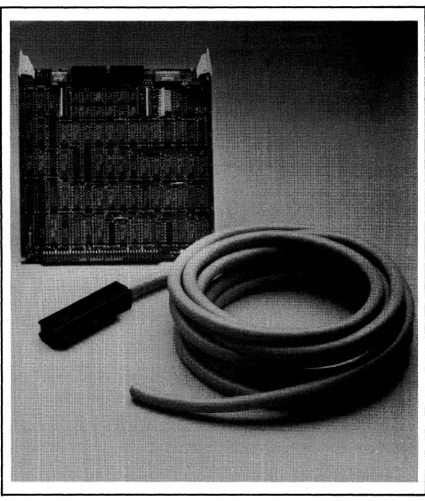
The HP 2 7112A General Purpose I/O Interface (GPIO) is shown in figure 1-1 and consists of a printed circuit assembly, a five-meter unterminated cable, and an installation manual.
FUNCTIONAL DESCRIPTION
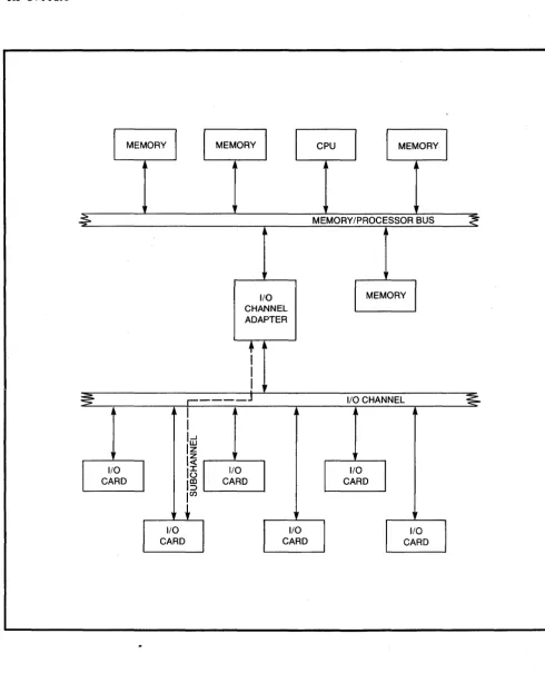
The GPIO provides 16-bit parallel data communication between a Hewlett-Packard computer sys-tem and a peripheral device.
Figure 1- 2 shows a typical Hewlett-Packard computer system using CHANNEL I/O and the GPIO. (CHANNEL I/O is a Hewlett-Packard standard defining the physical and electrical characteristics for an I/O system consisting of an I/O channel, an I/O channel adapter, and I/O cards. The GPIO is one of the I/O cards.)
Note that the computer system CPU and memory communicate directly along a Memory/Processor Bus (MPB). I/O data to/from peripheral devices reaches the CPU/memory through the I/O channel, the I/O channel adapter, and an I/O card such as the GPIO. The I/O data is received from and transmitted to peripheral devices by the I/O card, which converts device-specific data to a format compatible with the I/O channel, and thus the computer. The I/O channel interface (see figure
1-2) controls the flow of data traffic between the I/O channel and the memory/processor bus.
1
1
I...J
I/O
CHANNEL ADAPTER
I~
I~ ...--....1....--...
15
I~
1 (/) L . . - . _ _ _ ...
1/0
CARD
MEMORY/PROCESSOR BUS
[image:9.615.63.554.66.672.2]HP 27112A
EQUIPMENT SUPPLIED
The standard HP 2 7112A General Purpose I/O Interface consists of the following items (see figure 1-1 ):
GPIO interface card, part number 27112-60001
Five-meter unterminated cable, part number 27112-63002
_ ellS
Lit j:f' ::wg
/?-O ..
/hrS
,.."
J)v tJ()Nr cl'f
$k-t:.-SO Co /l.J7>u crof'l-. c!it.
.l.b /fW6 IiNN~-tJ (c)tfJl
2-? -If W 6; D /lAIN I4.J I (7.
C'
HP)7112A Installation Manual, part number 27112-90001The following options are available with the HP 2 7112A product:
001 Replaces unterminated cable (part number 27112-63002) with a 2.S-meter HP 9885 disc in-terface cable, part number 27112-63003
IDENTIFICA TION
The Product
Up to five digits and a letter (2 7112A in this case) are used to identify Hewlett -Packard products. The digits identify the product; the letter indicates the revision level of the product.
Interface Card
The interface card supplied with the HP 2 7112A is identified by a part number on the card. In addi-tion to the part number, the card is further identified by a letter and a four-digit date code (e.g., C-2308). This designation is placed below the part number. The letter identifies the version of the etched circuit on the card. The date code (the four digits following the letter) identifies the electrical characteristics of the card with components mounted. Thus, the complete part number on the GPIO card could be:
27112-60001 C-2308
If the date code stamped on the card does not agree with the date code on the title page of this
Manuals
The Installation Manual (part number 27112-90001), supplied with the HP 27112A product) and this manual (HP 2 7112A Technical Reference Manual, part number 27112-90003) are identified by name and part n urn ber (note that this manual is part. of the HP 271 32A Technical Reference Package). The
name, part number, and pUblication date are printed on the title page of each manual. If the manual
is revised, the publication date is changed. In this manual, the "Printing History" page (page ii) records the reprint dates. Printing history information for the Installation Manual is printed on the title page.
SPECIFICA TIONS
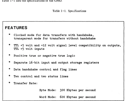
Table 1-1 lists the specifications of the GPIO.
Table 1-1. Specifications
FEATURES
*
*
*
*
*
*
*
Clocked mode for data transfers with handshake, transparent mode for transfers without handshake
TTL
+5
volt and +12 volt signal level compatibility on outputs, TTL+5
volt inputsPositive true or negative true logic
Separate 16-bit input and output storage registers
Data handshake control and flag lines
Two control and two status lines
Transfer Rate:
Byte Mode: 300 Kbytes per second
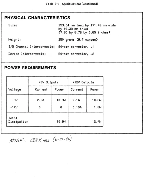
[image:11.617.50.494.273.627.2]Table 1-1. Specifications (Continued)
PHYSICAL CHARACTERISTICS
Size:
193.04 rrm long
by171.45 rrm wide
by
16.38 rrm thick
(7.60
by6.75
by0.65 inches)
Weight:
250 grams (S.7 ounces)
lID
Channel Interconnects: SO-pin connector, J1
Device Interconnects:
50-pin connector, J2
POWER REQUIREMENTS
+5V Outputs
+12V Outputs
Vol tage
Current
Power
Current
Power
+5V
2.2A
10.g.J
2.1A
10.SW
+12V
00
o
.15A
1 .8W
Total
Dissipation
10.g.J
12.4W
[image:12.618.74.555.84.741.2]INSTALLATION
1-~---~[[]
This section provides information on installing and checking the operation of the GPIO.
COMPUT A TION OF CURRENT REQUIREMENTS
The GPIO interface card obtains its operating voltages from the computer power supply through the I/O channel. Before installing the card, it is necessary to determine whether the added current will overload the power supply. The current requirements of the GPIO card are listed in the power requirements entry of table 1-1. Current requirements for all other I/O cards can be found in the appropriate Technical Reference Manuals.
LOGIC LEVELS
Peripheral device interface outputs are 7 5453B open-collector drivers with pull up resistors for 5-volt or 12-volt levels. The pullup voltages are determined by jumpers which select 5-volt or 12-volt
operation, depending on where the jumper is installed. If a jumper is installed in the 5-volt position,
the output voltage is + 5V; if the jumper is installed in the 12-volt position, the output voltage is
+ 12V. The locations of the jumpers on the card, and the positions of the jumpers for 5-volt or
12-volt operation, are shown in figure 2-1. The jumpers are listed below with the signals they con-trol.
JUMPER
W1
W2
W3
SIGNAL
DDUT[15:81
DDUT[7:01
CTL[1:01, PCNTL, DIR, PRESET
The peripheral interface signals DIN[ 15:0] and PEND use 5-volt LS-TTL levels. The remaining
HP 27112A
LOGIC SENSE
All peripheral interface signals can operate either positive true or negative true.
Positive true signals are considered "asserted" when their voltage level is 2.4 to 5 volts above ground potential (i.e.) is "high"). They are considered "deasserted" when their voltage level is less than 0.8 volts above ground potential ("low").
Negative true signals are considered "asserted" when their voltage level is low, and are considered "deasserted" when their voltage level is high.
CONFIGURA TION SWITCH DEFINITIONS
Two sets of switches are used to configure the GPIO: an eight-switch assembly (SWl) selects the logic sense of the peripheral interface signals, and a five-switch assembly (SW2) controls the handshake operation.
Switch functions are listed in tables 2-1 and 2-2, and the locations of the switch assemblies on the GPIO card are shown in figure 2-1.
Switch settings should be as shown below When the GPIO card is installed in an HP 9000 Computer System and is connected to an HP 9885 Disc Drive. Other switch settings depend on the host system in which the GPIO card is installed and the peripheral device which is connected to the GPIO card.
HP 9885 Disc Drive
C
closed
o
open
1 2
C C
3
C
SW1
4 5 6 7 8
C C C 0 C
Data Input Register Clock Select
SW2
1 2 3 4 5
o
0 0 C 0The Data Input register may be clocked by one of three selectable clocking events during data transfers. The specific clock is determined by the mode selected by switches 4 and 5 on switch as-sembly SW2 as shown in table 2-3. Data is clocked eyery time a clocking event occurs eve!lifthe old
data has not J2~~Il_read. ',,- - --- -' "- -..
,--Mode 1 selects the transition of the peripheral interface signal PFLAG from the ready state to the busy state within the data transfer.
Table 2-1. Configuration Switch SW 1 Definitions
SWITCH ASSEMBLY SW1
-
LOGIC SENSE SELECTION
SWITCH
CONTROLS
OPEN
CLOSED
I-f! -;.. I LO:: I
S1
DINE15:0]
POSITIVE TRUE
NEGATIVE TRUE
r
S2
CTL[1 :0] and STS[1:0] POSITIVE TRUE
NEGATIVE TRUE
S3
PRESET
POSITIVE TRUE
NEGATIVE TRUE
S4
PD IR
II
5.s o<.-Tl:!]).:-W K.J TEPOSITIVE TRUE
NEGATIVE TRUE
S5
DOUTE15:0]
POSITIVE TRUE
NEGATIVE TRUE
S6
PEND
POSITIVE TRUE
NEGATIVE TRUE
S7
PFLAG
POSITIVE TRUE
NEGATIVE TRUE
BUSY
=
HIGH
BUSY
=
LOW
READY
=
LOW
READY
=
HIGH
S8
PCNTL
POSITIVE TRUE
NEGATIVE TRUE
ACTIVE
=
HIGH
ACTIVE
=
LOW
IDLE
=
LOW
IDLE
=
HIGH
Table 2-2. Configuration Switch SW2 Definitions
SWITCH ASSEMBLY SW2 -
HANDSHAKE CONFIGURATION
SWITCH
CONTROLS
OPEN
CLOSED
S1
BIDIRECTIONAL BUS ENABLE
DISABLED
ENABLED
S2
INTERNAL HANDSHAKE ENABLE
DISABLED
ENABLED
S3
PULSE HANDSHAKE ENABLE
DISABLED
ENABLED
[image:15.615.68.549.117.656.2]HP 27112A
E15
E16
W3
W2
r
JUMPER IN 5V POSITION+5~+12
rJUMPER IN 1.2V POSITION
+6~+12
[image:16.617.69.540.75.655.2]Table 2- 3. Switch Settings for Data Input Register Clock Selection
SWITCH
SW2 - S5
SW2 - S4
MODE
DATA CLOCKED ON
CLOSED
CLOSED
0
Backplane 5ync cycle completion
CLOSED
OPEN
1 JReady to bU5y edge of PFLAG_
(leading edge)
OPEN
CLOSED
(~
,,~BU5Y to ready edge of PFLAG
(trailing edge)
OPEN
OPEN
3Backplane 5ync cycle completion
-
(Note that this mode i5 the 5ame
as mode 0)
Full/Pulse Handshake Select
The peripheral interface signal PFLAG, in addition to functioning as handshake acknowlege, can
function as a peripheralliREADY" signal. If the peripheral requires that before a data transfer may
begin the peripheral must be ready, then IIFull mode" is required and "Pulse Modell must be disabled.
Internal Handshake
Internal handshake is used in applications where a two-wire handshake is not required. When internal handshake is enabled, a one-shot provides an internal FLAG signal, eliminating the need for the peripheral signal PFLAG. The internal FLAG will be asserted approximately 3 usec after PCNTL is asserted. You can increase this delay by adding an additional timing capacitor. The signal PCNTL is still available externally and may be used to clock data.
Bidirectional Bus Enable
[image:17.618.79.556.91.353.2]HP 27112A
PCNTL Sense
The peripheral interface signal PCNTL is positive true when the PCNTL switch is open and nega-tive true when the switch closed. The deasserted state of PCNTL indicates that a GPIO data transfer is idle, and the asserted state indicates indicates that it is active.
PFLAG Sense
The peripheral interface signal PFLAG is positive true when the PFLAG switch is open and nega-tive true when the switch is closed. The de asserted state of PFLAG indicates ready and the asserted state indicates busy.
PEND
Sense
The peripheral interface signal PEND is positive true when the PEND switch is open and negative true when the switch is closed.
DOUT[ 15: 0] Sense
The peripheral interface signals DOUT[ 15:0] are positive true when the DOUT[ 15:0] switch is open and negative true when the switch is closed.
PDIR
Sense
The peripheral interface signal PDIR is positive true when the PDIR switch is open and negative true when the switch is closed. PDIR is asserted when a Write_data_order is present.
PRESET Sense
The peripheral interface signal PRESET is positive true when the PRESET switch is open and nega-tive true when the switch is closed.
CTL and STS Signal Sense
The sense of the peripheral interface signals CTL[I:0] and STS[I:0] is controlled by the CTL &
STS switch. When the switch is open all the signals operate in positive true mode. When the switch is closed all the signals operate in negative true mode.
DIN[ 1 5: 0] Sense
TIMING CAPACITORS
There are two one-shots (E 15) on the GPIO card which generate the write delay and the internal
handshake delay.
Write Delay One-Shot
The write delay one-shot (see figure 6-1, quadrant E5 of sheet 2) provides approximately 100 nsec for the output data to settle between the time it is clocked into the output latch and the assertion of PCNTL. When extra long cables are used or when the peripheral requires additional settling time for the data, the delay can be increased by adding a capacitor between pins 1 and 4 of the socket at E 16.
The formula for the value of the capacitor required is:
C
=
(T - 100) / 1.5where
C
=
Additional capacitance (in pf)
T
=
Total time delay reguired (in nsec)
Internal Handshake Delay One-Shot
The internal handshake delay one-shot (see sheet 2, D7 of figure 6-1) provides a delay of ap-proximately 3usec between the assertion of PCNTL and the assertion of FLAG when the card is in
internal handshake mode. It has no effect when internal handshake mode is disabled. The delay can
be increased by adding a capacitor between pins 5 and 8 of the socket at E 16.
The formula for the value of the capacitor required is:
c
= (
T - 3000 ) / 3where
C
Additional capacitance (in pf)
T
=
Total time delay reguired (in nsec)
1/0
CHANNEL INTERFACE
All interface between the GPIO and the host computer occurs on the I/O channel. An 80-pin
con-nector (J 1) located on the GPIO mates with a receptacle on the I/O channel. Connections to J 1
UP 27112A
Table 2-4. I/O Channel Connector J 1
PIN NO.
SIGNAL MNEMONIC
SIGNAL DEFINITION
A1
---
Not u5ed
A2
DB14-
Data BU5, bit 14
A3
DB12-
Data BU5, bi t 12
A4
GND
Ground
A5
DB10-
Data BU5, bit 10
A6
DB8-
Data BU5, bit
8A7
GND
Ground
A8
DB6-
Data BU5, bi t 6
A9
DB4-
Data BU5, bit 4
A10
GND
Ground
A11
DB2-
Data BU5, bit 2
A12
DBO-
Data BU5, bi t 0
A13
GND
Ground
A14
AD2-
Addre55 BU5, bit 2
A15
ADO-
Addre55 BU5, bi t 0
A16
GND
Ground
A17
DOUT-
Data Out
A18
BPO-
BU5 Primitive, bit 0
A19
CEND-
Channel End
A20
SYNC-
Synchronize
A21
GND
Ground
A22
---
Not u5ed
A23
GND
Ground
A24
BR-
Bur5t
A25
DBYT-
Device Byte
A26
MYAD-
My
Addre55
A27
GND
Ground
A28
---
Not u5ed
A29
---
Not u5ed
A30
---
Not u5ed
A31
---
Not u5ed
A32
---
Not u5ed
A33
PPON
Primary Power On
A34
GND
Ground
A35
---
Not u5ed
A36
---
Not u5ed
A37
---
Not used
A38
y+12
+12V
A39
---
Not u5ed
[image:20.613.68.551.106.716.2]Table 2-4. I/O Channel Connector Jl (Continued)
PIN NO.
SIGNAL MNEMONIC
SIGNAL DEFINITION
B1
---
Not u5ed
B2
DB15-
Data Bus, bi t 15
B3
DB13-
Data Bus, bit 13
B4
GND
Ground
B5
DB11-
Data Bus, bi t 11
B6
DB9-
Data Bus, bit
9B7
GND
Ground
B8
DB7-
Data Bus, bit 7
B9
DB5-
Data Bus, bit 5
B10
GND
Ground
B11
DB3-
Data Bus, bit 3
B12
DB1-
Data Bus, bit 1
!
B13
GND
Ground
B14
AD3-
Address Bus, bit 3
815
AD1-
Address Bus, bit 1
B16
GND
Ground
B17
UAD-
Unary Address
B18
BP1-
Bus Primitive, bit 1
B19
---
Not u5ed
B20
POLL-
Poll
B21
GND
Ground
822
IOSB-
I/O Strobe
823
GND
Ground
824
ARQ-
Attention Request
825
DEND-
Device End
826
IFC-
Interface Clear (Reset)
827
GND
Ground
828
---
Not used
829
---
Not used
830
---
Not used
B31
---
Not used
832
---
Not used
833
---
Not used
B34
GND
Ground
835
---
Not used
B36
---
Not u5ed
837
---
Not u5ed
838
+12
+12V
839
---
Not u5ed
[image:21.620.74.552.118.682.2]HP 27112A
PERIPHERAL DEVICE INTERFACE
A cable from connector J2 on the GPIO provides interface between the GPIO and the peripheral
device. Connections to J2 are listed in table 2- 5.
Table 2- 5. Device Connector J2
GPIO
9885
CONN.
SIGNAL
WIRE
CONN.
SIGNAL
PIN NO.
MNEMONIC COLOR
PIN NO.
DEFINITION
A1
Shield
Drain
1
Chassis Ground
A2
DOUT 15
BRN
18
Data Output, bit 15
A3
DOUT 14
RED
19
Data Output, bit 14
A4
DOUT 13
ORN
20
Data Output, bit 13
AS
DOUT 12
YEL
21
Data Output, bit 12
A6
DOUT 11
GRN
22
Data Output, bit 11
A7
DOUT 10
BlU
23
Data Output, bit 10
A8
DOUT 9
VIO
24
Data Output, bit 9
A9
DOUT 8
GRY
25
Data Output, bit 8
A10
DOUT 7
WHT
26
Data Output, bit 7
A11
DOUT 6
WHT-BLK
27
Data Output, bit 6
A12
DOUT 5
WHT-BRN
28
Data Output, bit 5
A13
DOUT 4
WHT-RED
29
Data Output, bit 4
A14
DOUT 3
WHT-ORN
30
Data Output, bit 3
A15
DOUT 2
WHT-YEL
31
Data Output, bit 2
A16
DOUT 1
WHT-GRN
32
Data Output, bit 1
A17
DOUT 0
WHT-BLU
33
Data Output, bit 0
A18
GND
WHT-VIO
8
Ground
A19
PCNTL
WHT-GRY
10
Peripheral control
A20
PDIR
WHT-BLK-BRN 15
Peripheral direction
A21
GND
WHT-GRN-BlU
NIC
Ground
A22
PRESET
WHT-BLK-RED 5
Peripheral reset
A23
CTlO
WHT-BLK-ORN 4
Control Output Bus, bi t 0
A24
CTl1
WHT-BLK-YEL 6
Control Output Bus, bi t 1
[image:22.612.63.549.89.734.2]Table 2- 5. Device Connector J2 (Continued)
GPIO
9885
CONN.
SIGNAL
WIRE
CONN.
SIGNAL
PIN NO.
MNEMONIC COLOR
PIN NO.
DEFINITION
B1
Shield
Shield
1
Ground Shield
B2
DIN 15
WHT-BLK-VIO 35
Data Input, bit 15
B3
DIN 14
WHT-BLK-GRY
36Data Input, bit 14
B4
DIN 13
WHT-BRN-RED 37
Data Input, bit 13
B5
DIN 12
WHT-BRN-ORN
38Data Input, bit 12
B6
DIN 11
WHT-BRN-YEL
39Data Input, bit 11
B7
DIN 10
WHT-BRN-GRN 40
Data Input, bit 10
B8
DIN 9
WHT-BRN-BLU 41
Data Input, bit 9
B9
DIN 8
WHT-BRN-VIO 42
Data Input, bit 8
B10
DIN 7
WHT-BRN-GRY 43
Data Input, bit 7
I
B11
DIN 6
WHT-RED-ORN 44
Data Input, bit 6
I
B12
DIN 5
WHT-RED-YEL 45
Data Input, bit 5
B13
DIN 4
WHT-RED-GRN 46
Data Input, bit 4
B14
DIN 3
WHT-RED-BLU 47
Data Input, bit 3
B15
DIN 2
WHT-RED-VIO 48
Data Input, bit 2
B16
DIN 1
WHT-RED-GRY 49
Data Input, bi t 1
B17
DIN 0
WHT-ORN-YEL 50
Data Input, bi t 0
B18
GND
WHT-ORN-GRN 9
Ground
B19
PFLAG
WHT-ORN-BLU 13
Peripheral flag
B20
GND
WHT-ORN-VIO 3
Ground
B21
PEND
WHT-ORN-GRY 16
Peripheral end
B22
---
WHT-YEL-GRN 17
Not used
B23
STS 0
WHT-YEL-BLU 14
Status Input Bus, bit 0
B24
STS 1
WHT-YEL-VIO 7
Status Input Bus, bit 1
B25
GND
WHT-YEL-GRY 12
Ground
---
---
N/C
34
Not used
N/C
---
BLK
2
Not used
[image:23.617.67.555.51.742.2]HP 27112A
I'NST ALLA TION
I
CAUTIONI
ALWAYS ENSURE THAT THE POWER TO THE BACKPLANE IS OFF BEFORE INSER TING OR
REMOVING THE GPIO CARD AND CABLE.
FAILURE TO DO SO MAY RESULT IN DAMAGE TO THE GPIO.
To install and check the operation of the GPIO card, follow the steps below in the order given:
1. Determine if your computer system can supply the power needed for the GPIO card. Refer to Section I, table 1-1 for power requirements.
2. Install jumpers in WI, W2, and W3, depending on whether S-volt or 12-volt logic levels are to be used. The locations of WI, W2, and W3, and the positions of the jumpers for +S-volt or + 12-volt operation are shown in figure 2-1.
3. Set the card's switches for proper operation in your system. Refer to tables 2-1, 2-2, and 2-3 for switch information. Actual switch settings will vary according to the computer system and the device which is connected to the GPIO card. However, switch settings for the HP 9885 disc drive (a typical device used with the GPIO) are shown below:
DEVICE SW1 SW2
1 2 3 4 5 6 7 8 1 2 3 4 5
HP 9885 Disk Drive
C C C C C C 0 C 0 0 0 C 0o
=
open
C
closed
4. There are two one-shots (E IS, see figure 2-1) on the GPIO card which generate the write delay and the internal handshake delay. The write delay one-shot provides approximately 100 nsec for the output data to settle. When extra long cables are used, or when the peripheral device requires additional settling time for the data, the delay can be increased by adding a capacitor between
pins 1 and 4 of the socket at E 16 (see figure 2-1 for location of E 16).
The formula for selecting the capacitor value is:
C
=
(T -
100)/1.5The internal delay one-shot provides a delay of approximately 3 usec between the assertion of PCNTL and the assertion of FLAG. The delay can be increased by adding a capacitor between
pins 5 and 8 of the socket at E 16 (see figure 2-1 for location of E 16).
The formula for the value of the capacitor is:
C = (T - 3000)/3
where,
C additional capacitance (in pf)
T total time delay reguired (in nsec)
5. Install the card in the appropriate slot in the computer. Refer to the computer system
in-stallation manual to determine the correct slot.
6. Connect the cable, supplied with the card, from J2 on the card to the peripheral device. If you have the test hood, which exercises more of the card's circuitry, and can be ordered (Hewlett-Packard part number 1251- 8003), connect it to J2 instead of connecting the cable.
NOTE
A "grounding grommet" on the interface cable allows the cable shield to be "grounded" at that point in some applications. Refer to your computer installation manual.
7. Turn on computer system power.
8. Run the card verification program. Refer to the appropriate host computer system manual for information on running this program.
9. If a test hood was used, turn off computer power and remove the test hood. Connect the cable
and, if necessary, reset the switches for your application.
RESHIPMENT
If the GPIO is to be shipped to Hewlett-Packard for any reason, attach a tag identifying the owner
and indicating the reason for shipment. Include the part number of the GPIO.
Pack the card in the original factory packing material, if available. If the original material is
PRINCIPLES OF OPERATION
1-~---~~
INTRODUCTION
The GPIO provides 16-bit parallel data communications between the I/O channel and a peripheral device. The devices supported by the GPIO fall into two categories: "word devices" and "bit devices". Word devices associate all the data communicated in parallel as one logical unit of information. Bit devices use the parallel bits independently.
Word devices that are commonly supported by the GPIO are paper tape readers and punches, card readers, line printers, disc drives (including flexible discs), and magnetic tape drives. These devices usually combine several units or words into records which have unit logical significance. These records are referred to as "messages".
Bit devices that are commonly supported by the GPIO are typically involved in low-level control operations. Relay sequencers and contact closures are bit-oriented. For example, relay one has a function independent of relay two even though data bits one and two are presented together by the GPIO.
FUNCTIONAL THEORY OF OPERA TION
A functional block diagram of the GPIO is shown in figure 3-1. Reference also should be made, as necessary, to the schematic logic diagram contained in figure 6-1. Note that figure 6-1
con-sists of four sheets. References to this figure will be as follows: l-A3, 6-1, 2-C8, 6-1, etc., where
the first number, 1 through 4, refers to the sheet number, the combination of letters A through E
and numbers 1 through 8 (A3, C8, etc.) refer to the quadrants on the sheet, and 6-1 refers to the
...J W Z Z ~ I U o ::::: RST
I PPON
I
UADAD
r
1.-
MYAD1=
DBYT...
[image:27.618.65.545.53.651.2]... BR
...
I
I
I POLL
I
I
SYNCI
1
BPI
I
DB~
...
... ARO
...
I
L
..
DEND~
...
-...
...
...
....
...
...
..
...
..
....
--...-... ...+
~ ~ ,.. OUTPUTADDRESS DATA
~
DECODE CIRCUIT
CIRCUIT
-..--
...
.A
"-'r
INPUT DATA
...
CIRCU!T--....-COMMAND
~
r--+
PROCESSING CIRCUIT
....
...
STATUS
t
AND L ...r
CONTROLCIRCUIT
...
..
,
SROAND ARO
CONTROL
....
...
...
...I
DO[.:I~)
I
I
I
... DI[0:15]
I
K ... I
-I
I
CTL[~:l]
....
..
_ STS[0:1]
!
...
J
PDIR
-PCNTL .... 1
PFLAG .... -,
PEND
-,
w U
>
wHP 27112A
The GPIO consists of six functional sections, as follows:
Address Decode Circuit (ADC)
Command Processing Circuit (CPC)
SRQ and ARQ Control (SAC)
Input Data Circuit (IDC)
Output Data Circuit (ODC)
Status and Control Circuit (SCC)
Address Decode Circuit
The components comprising the Address Decode Circuit (ADC) are shown on sheet 1 of figure 6-1. The ADC learns the GPIO device address at power up or after a reset. Once having learned the ad-dress, the ADC screens all addressed I/O channel bus operations and informs the Command Processing Circuit whether or not the current I/O channel operation is addressed to the GPIO. Finally, the ADC signals to the I/O channel interface that it is responding to the current ad-dressed I/O channel operation.
Command Processing Circuit
The CPC (figure 6-1, sheets 1 and 4) interprets channel operations and initiates the appropriate opera-tion throughout the GPIO. Two classes of operaopera-tions are interpreted by the CPC: GPIO-I/O channel operations and peripheral device-I/O channel operations. GPIO-I/O channel operations manipUlate the GPIO and affect GPIO interaction with the I/O channel, but have no direct effect on the peripheral device. Peripheral device-I/O channel operations are intended to transfer data to or from the device, or to directly affect the device; these are the primary operations of the GPIO.
SRQ and ARQ Control
Input Data Circuit
The Input Data Circuit (IDC) consists of a 16-bit register and 16 line receivers (see 3-B3, 6-0. The line receivers (with selectable data sense) connect directly to the peripheral device through connector J2. The IDC is clocked by the device handshake logic of the SRQ and ARQ Circuit except on input
DC"'- following mode. The Command Processing Circuit enables the outputs of the register, which transfers
e"U)Qe
"---the 16-bit incoming data, via the GPIO internal data bus (signals IDBO- through IDB 15-), to the I/O~\o ') channel when this bus is ready for read data.
ok
o
Output Data Circuit
The Output Data Circuit (ODC) consists of a 16-bit register (Output Data register) and 16 line drivers with selectable data sense (see 3-B5, 6-1). The line drivers connect directly to the peripheral device through connector J2. When the I/O channel has write data ready for transfer, the ODC is clocked by the Command Processing Circuit and the data is transferred via the internal data bus (signals IDBO-through IDB15-), the register, the line drivers and connector J2 to the peripheral device.
Status and Control Circuit
The Status and Control Circuit (SeC) consists of the Status register, Control register, line drivers, and line receivers (see 3-E2 to 3-E7, 6-1). The SCC facilitates control of the peripheral outside the data path by examining or asserting status and control signals as appropriate.
SIGNAL DEFINITIONS
The following paragraphs describe GPIO/peripheral device interface signals. Information included for each signal includes the signal name, where it originates, where it goes, its function, timing data, and where it can be found on the schematic logic diagram of figure 6-1 in Section 6. Pin connec-tions for the signals (connector J2) are presented in table 2-4, Section 2.
HP 27112A
PDIR
Full Hame:
Peripheral Data Direction
Driven
By:
GPIO
Received
By:
Peripheral device
Function:
PDIR signals when the GPIO
is set for Write-Pata
operations)
thus signalling the peripheral device that
the GPIO is going to assert DOUT[15:0J.
Primary use of
PDIR
occurs
in
bidirectional
data
bus
cable
configurations.
Timing:
PDIR is aS5erted upon receipt of a Write Data order.
PDIR
is deasserted when any order other than Write_Data
is received, or when GPIO reset conditions occur.
Schematic
Location:
DIN [15:0]
Sheet 2) B8
Full Hame:
Data Input Bus
Driven
By:
Peripheral device
Received
By:
GPIO
Function:
Data Input Bus receive5 data from the peripheral device.
Timing:
Data may be driven onto the DIN by the peripheral device
at any time.
Refer to the paragraph "Input Hand5hake
Timing" for additional timing data on Data Input Bus
operation.
Schematic
DOUT
Full Name:
Data Output Bus
Driven
By:
GPIO
Received
By:
Peripheral device
Function:
Timing:
Schematic
Location:
STS [1:0]
Data Output Bus transmits data from the GPIO
to the
peripheral device.
If the bidirectional bus switch (SW2-1) is closed, DOUT
signals
are
active
only when. PDIR
is asserted.
Otherwise, DOUT signals are always
active.
When
operating a bidirectional bus, DOUT[15:0] should be set
to a voltage high (regardless of logic sense) when input
data is transmitted.
Sheet 3, AS through DB
Full Name:
Status Input Bus
Driven
By:
Peripheral device
Received
By:
GPIO
Function:
Statu5 Input Bus provides an auxiliary data path and an
event detection path from the peripheral device. The
data path is normally used to receive peripheral device
status pertinent to the ongOing data transfer. Event
detection may be used to alert the host CPU
that a
statu5
transition
has
occured.
Schmitt trigger
receivers are used on these inputs.
Timing:
Status Input Bus signals may be driven by the peripheral
device at any time.
In order to cause an interrupt,
event detection must be enabled before operation. Refer
to the "Interrupt ARQs" paragraph for additional timing
data on Status Input Bus operation.
Schematic
HP 27112A
CTL [1:0]
Full Name:
Control Output Bus
Driven
By:
GPIO
Received
By:
Peripheral
devic~Function:
Control Output Bus provides an auxiliary data path to
the peripheral device. This data path is normally used
to transmit control information pertinent to the ongoing
data transfer.
Timing:
Control Output Bus signals are always active.
Schematic
Location:
PFLAG
Sheet 3, E8
Full Name:
Peripheral Flag
Driven
By:
Peripheral device
Received
By:
GPIO
Function:
Peripheral Flag signals completion of the data transfer
in progress (note that it does not signal termination
of the data transfer
interaction).
When
FULL
handshake mode
is selected, Peripheral Flag indicates
when the peripheral device is willing to partIcipate in
the next data transfer.
Timing:
Peripheral Flag may be driven at any time by the
peripheral device.
Refer to the IIHandshake Timing"
paragraph for additional timing data on Peripheral Flag
operation.
Schematic
PCNTL
Full Name:
Peripheral Control
Driven
By:
GPIO
Received
By:
Peripheral device.
Function:
Peripheral Control signals the beginning of a data
transfer.
(Note:
No signal defines the beginning of a
sequence of transfers; PCNTL defines the beginning of
each data exchange.)
Timing:
Peripheral Control
is asserted for each data
bus
transfer. Refer to the "Handshake Timing" paragraph for
additional timing data on Peripheral Control operation.
Schematic
Location:
PEND
Sheet 2, B8
Full Name:
Peripheral End
Driven
By:
Peripheral device
Received
By:
GPIO
Function:
Timing:
Schematic
Location:
Peripheral End signals termination of the current data
transfer interaction.
Peripheral End timing is the same as Data
Input Bus
timing, and may be asserted at any time.
HP 27112A
PRESET
Full Name:
Peripheral Reset
Driven
By:
GPIO
Received
By:
Peripheral device
Function:
Timing:
Schematic
Location:
PRESET signals the peripheral device to return to a
power-up state of readiness.
PRESET is asserted whenever the
liD
channel asserts
Reset
(RST),
or asserts Power On (PPON), or performs a
Write_Control (Device Clear) operation.
Sheet 2, B8
HANDSHAKE TIMING
Data is transferred between peripheral device and I/O channel (backplane) in a synchronous man-ner using the backplane signal SRQ and peripheral signals PCNTL) PFLAG) PDIR) and PEND. SRQ is asserted by the GPIO card when it is ready for the next backplane data transfer. PCNTL and PFLAG provide a two-line handshake for data transfers to the device. PDIR is driven by the GPIO to indicate the direction of data. PEND is asserted by the device to request termination of the transfer.
Data handshake timing depends on whether input data or output data is transferred) and whether the peripheral simply acknowledges data transfer or if data transfer must be postponed until the peripheral is ready. If the peripheral simply acknowledges data transfer) the handshake mode is
referred to as "Pulse ". If data transfer must be postponed until the peripheral is ready to
con-tinue the handshake mode is referred to as "Full".
If an external handshake is not required by the application) the internal handshake can be enabled
and a one-shot will provide an internal FLAG signal to replace PFLAG. The internal FLAG will be asserted approximately 3 usec after PCNTL is asserted. You can increase this delay by adding an
additional timing capacitor. If Internal Handshake Mode is enabled) then in the following
descriptions the internal FLAG replaces PFLAG and the card operates in Pulse Handshake Mode regardless of the switch setting.
If a handshake is not required and the delay incurred with internal handshake is undesirable) the PCNTL output can be connected to the PFLAG input. In this case the pulse width of PCNTL/PFLAG may be very short) so to ensure reliable operation it is recommended that only input following clocking mode· be used (Input Clocking Mode No. 0 or No.3).
PCNTL signals to the peripheral that the transfer has begun and the peripheral responds by gating read data onto the lines or accepting write data. When the data transfer is complete (i.e., the peripheral is sourcing read data or has accepted write data), the peripheral asserts signal PFLAG. At this point, if the "Pulse" handshake mode was selected, the GPIO card may begin the next data
transfer. If the "Full" handshake mode was selected, the GPIO card will wait until the ,signal PFLAG
returns to the ready state (i.e., PFLAG is deasserted).
Data transfers continue under PCNTL, PFLAG control until a terminating condition arises. One of two conditions will normally terminate data transfers: The channel asserts CEND (channel end) if it has detected an end condition (such as character match or transfer count completed), or the peripheral asserts signal PEND if it detects an end condition.
Output Handshake Timing
Figure 3-2 illustrates output data transfer timing with the GPIO in full handshake mode. All conditions significant to output data transfer are shown, including: duration of the or-der(write_data); backplane write data transfers; the backplane line CEND; GPIO lines SRQ, DOUT[15:0], PDIR, and PCNTL; and the peripheral line PFLAG.
PDIR INPUT
OUTPUT
WRITE DATA ORDER ~---+---~---4~)
WRITE DATA OPERATION (IOSBI DOUT [15:11] CEND
SRQ
ACTIVE
I I , I
WRITE DELAY
PCONT
IDLE I---~.
PFLAG BUSY
READY
1---...1
~--INITIATION CYCLE ---tl~-CONTINUATION CYCLE
Figure 3-2. Output Data Transfer Timing
/
[image:35.612.68.546.335.715.2]HP 27112A
The diagram describes the initiation, continuation (normal transfer), and the termination
cycles of an output data transaction. A transfer cycle follows a prescribed sequence of events as follows:
1. Initiation begins when the Write_order (write_data) is received. The PDIR line is asserted to show that an output data transaction is in progress. The PEND latch on the GPIO card is cleared to remove any old end conditions. SRQ is asserted unless the GPIO is in "full"
hand-shake mode and PFLAG is not ready) and GPIO waits for the fIrs a:tjCva1Ue:~~ f1 j ~
2. Write_data strobes the write data into the Output Data register and the data appears on DOUT[15:0].
vI!
,1\ ,,11
3. SRQ is deasserted and, after the write delay (settling time for outputs) PCNTL is asserted to
indi-cate data available to the peripheral. The GPIO then waits until ...
/' f3,(Jf:, '1
4. PFLAG is asserted by the peripheral to indicate data accepted .
... lv"t
5. PCNTL is then deasserted to acknowlege data acceptance. At this point the transfer is complete
if the pulse handshake mode was selected. If full handshake mode was selected, then the
GPIO card idles until PFLAG becomes ~ (deasserted).
6. The GPIO will reassert SRQ to indicate that the transfer has completed.
a. If CEND and DEND are deasserted, the process repeats at step 2 with the next write_data
operation.
or,
b. If the I/O channel asserted CEND (channel end) with the current data operation, no
more output data transfers are expected.
or,
c. If the peripheral asserted PEND (peripheral end) with the current data operation; the process
will repeat at step 2., the GPIO will assert DEND (device end) with the backplane transfer,
and the transaction will stop after step 6. is reached again.
Input Handshake Timing
PDIR
PEND CEND SRO PCONT
fCNiL-PFLAG
- - . . . - I ... CONTINUATION CYCLE TERMINATION CYCLE
CD READY TO BUSY TRANSITION OF PFLAG
I
@BUSY BACK TO READY TRANSITION OF PFLAG@ END OF BACKPLANE OPERATION PRIOR TO INPUT REGISTER + PEND CLOCKING READ_DATA OPERATION
Figure 3- 3. Input Data Transfer Timing
The diagram describes the initiation, continuation (normal transfer), and termination cycles of an input data transaction. A transfer cycle follows a prescribed sequence of events as follows:
1. Initiation begins when the Write_order (read_data) is received. The PDIR line is deasserted
to show that an input data transaction is in progress.
2. SRQ is deasserted and PCNTL is asserted to indicate that the GPIO is ready for data from the
peripheral.:tqhe GPIO then ~s.~
3. Data is sourced by the peripheral.
4. PFLAG is asserted by the peripheral to indicate that data is available. In clocking mode No. I,
data will be clocked at the time of PFLAG (indicator No. 1).
S. PCNTL is then deasserted: to acknowlege data acceptance. If pulse handshake mode was selected,
[image:37.612.45.543.75.445.2]be-HP 27112A
7. The channel performs a Read_data. In clockin mode 0 or 3, the data will have been clocked in
by the end of the backplane operation~.~ior tv the Read Data. If CEND and DEND are
deas-serted, the GPIO will assert SRQ when
ine~le complet~
to prompt the channel to Read_data,and the process repeats at step 2.
or,
a. If the channel asserted CEND (channel end) with the Read_data, no more input data
transfers are expected, and a new handshake with the device is not initiated.
or,
b. If the peripheral asserted PEND at the time DIN[ 15:0] was clocked, no more input data
transfers are expected, the GPIO asserts DEND (device end) during the Read_data, and a new handshake with the device is not initiated.
Abnormal Termination
The I/O channel may cause an abnormal termination at any time by issuing an abort command (refer to Write_command) which immediately terminates any data transfer in progress and disconnects the I/O channel. The peripheral can perform a similar function by stopping any transfers in progress (i.e., not asserting PFLAG in response to PCNTL), and by causing an interrupt, on STS[l] or STS[O] in order to cause an ARQ. (Note that interrupts on that input must be enabled, refer to
the paragraph "Control Output Registerll
.) A program must then respond to the ARQ by issuing an
a bort command.
ARQ
There are two sources of ARQ (Attention Request) on the GPIO card: acknowledgement of the abort command (ADT), and asynchronous event sense (AES).
Aborted ARQs
If the GPIO card has a valid subchannel (i.e., a transaction is in progress) and it receives an abort
command, it will abort the subchannel and drive the ARQ bit in the Sense register. The card will not
respond to SRQ polls. If ARQs are enabled (ARE), the card will also assert the ARQ signal and respond
to ARQ polls. The card will respond to a read_status with the ADT status byte. The low four bits of the status byte will contain the subchannel address. If there is no valid subchannel, nothing will happen.
Interrupt ARQs
dis-When an interrupt is detected, the GPIO card will assert the ARQ bit in the Sense register. If
ARQs are enabled, it will also assert the ARQ signal and respond to ARQ polls. The card will respond to read status with an AES status byte unless an ADT status byte is also present. If an ADT status byte and an AES status byte are both present, the first read status will return the ADT status and ARQ wilLremain until the AES byte is read by a second read status.
Clearing ARQ
Co-nditions
A reset to the card (PPON, IFC, or DCL) resets INT.EN, INTO, and INT 1. It also removes any pending AES or ADT status bytes and deasserts ARQ.
An ADT status byte is cleared by reading it, by resetting the GPIO card, or by connecting a new subchannel. The last condition should not occur in normal CHANNEL I/O operation. An AES status byte is cleared by reading it, by resetting the card, or by disabling the interrupt that caused it.
The GPIO card is the slave in a master/slave relation with the I/O channel adapter. As such, backplane operation is driven by the channel adapter via standard CHANNEL I/O bus operations. All CHANNEL I/O level 1 bus operations are supported by the GPIO card. Bus operations are specified by I/O channel signals SYNC, POLL, BP[1:0], DOUT, and AD[3:0] (see table 3-1).
Additionally, the GPIO card will respond to a special backplane operation for purposes of learning an operating (card) address.
Table 3-1. Operations Summary
SYNC
POLL DOUT BP[ 1 : 0]
AD[3:0]
BACKPLANE OPERATION
0
X1
00
card address
assign_address
*
0
1
X00
X poll_sr~grp_O0
1
X01
X poll_sr~grp_10
1
X10
X poll_ar~grp_O0
1
X11
Xpoll_arq....grp_1
1
0
0
00
subchannel address
read-data
1
0
001
card address
read_sense
1
0
010
Xno_operation
1
0
0
11
card address
read_status
1
0
1
00
subchannel address
write_data
1
0
1
01
card address
write_control
1
0
1
10
subchannel address
write_order
1
0
1
11
card address
-
write_comnand
[image:39.617.60.552.368.760.2]HP 27112A
ADDRESS ASSIGNMENT OPERATION
Address assignment is required for the GPIO card to qualify backplane operations. The GPIO card address is programmed by the I/O channel via a special Write_data operation. The Write_data
is additionally qualified by backplane signal VAD and the GPIO card state "no adapter address
cur-rently assigned".
A qualified Write_data operation assigns the GPIO card the address-specified by I/O channel signals AD[ 3:0], and the card does not use the signals DB[ 15:0]. Signals DB[ 15:0] may be used, however, to
drive signal VAD on the I/O channel itself.
The address assignment must be performed before any other I/O channel operation can be recognized. Also, once an address is assigned, further address assignment operations will be ignored until the I/O channel issues IFC or PPON to the GPIO card;
POLL OPERA TIONS
Poll operations, SRQ or ARQ, directly reflect requests for subchannel or GPIO card service, respectively. The frequency of poll operations determines the maximum throughput and worst case latency in data transfer.
Only one of the poll operations of each type, SRQ and ARQ, will be responded to by the GPIO card. The response depends on the previously assigned addresses for subchannel and card (see table 3-2).
Table 3-2. Poll Operations
BACKPLANE OPERATION
REQUIRED ADDRESS
*
I
poll_srCl-grp_O
subchannel address 0-7
I
poll_srCl-grp_1
subchannel address 8-15
iI
i
II
po ll_BrCl-grp_O
card address 0-7
I
poll_arCl-grp_1
card address 8-15
[image:40.615.74.566.451.651.2]If no subchannel address or card address has been assigned by the I/O channel adapter, .no SRQ or ARQ (respectively) response will be generated by the GPIO card.
OUT -OF -SUBCHANNEL OPERATIONS
Card operations, read_sense, write_control, read_status, and write_command directly control the GPIO card and its operation with the I/O channel. The sense and control operations affect signal)evel interaction, while status and command operations affect subchannel interaction.
Read Sense
Read_sense may occur at any time and immediately gates the sense byte to the backplane. The sense byte format is:
7 6 5 4 3 2 1 0
RFC PST PRE NMI
r ARE
r ARQ
where,
RFC
=
Ready For Command.
Thi5 bit i5 ALWAYS s55erted by
GPIO.
PST
=
Passed Self Test. This bit is ALWAYS aS5erted by GPIO.
PRE
=
Present. Thi5 bit i5 ALWAYS a55erted by GPIO.
NMI
=
Non-Maskable Interrupt. Thi5 bit i5 NEVER a55erted by
GPIO.
ARE
=
Attention Reque5t5 Enabled. Thi5 bit is aS5erted when
GPIO is enabled to re5pond to arq polls.
ARQ
=
Attention Reque5t. Thi5 bit i5 s5serted when GPIO
i5
requesting attention.
HP 27112A
Write_Control
Write_control may: occur at any time and immediately invokes the control action specified by the control byte. The control byte format is:
7 6 5 4 3 2 1 0
r
r DCl DEN NMK RQA ARE ARD
where,
r
=
re5erved
DCl
=
Device Clear. Thi5 bit e5tablishe5 an addre5sed device
clear condition.
DEN
=
Device Enable. Thi5 bit terminates an addressed device
clear condition.
NMK
=
Non-Maskable_interrupt acknowledge.
Ignored by GPIO.
RQA
=
Request Attention.
Ignored by GPIO.
ARE': Attention Request Enable. Sets the GPIO ARE
flip-flop
enabling assertion of the ARQ I/O channel signal.
ARD
=
Attention
flip-flop
;j
ignal.
Request Disable.
disabling a5sertion
NOTE
Resets the
GPIO
ARE
of the ARQ I/O channel
If both DeL and DEN are asserted, the state of the
Read Status
Read_status may only occur after an Attention Request (ARQ), because it may reset the reason for ARQ. The status byte indicates the reason for ARQ. The format of the status byte is:
7161514 31
21
11
0coding
n
*
where)
STATUS
RFC
AES
ADT(n)
CODING
**
o
=
=
Ready For Command.
for command and
!Status.
GPIO is
will not
ALWAYS
ready
arq with RFC
Asynchronous Event Sensed.
Indicates that
the GPIO has sensed an interrupt on STS[11
or STS[Ol. The interrupt must be enabled
in order to cause this condition.
3
=
Aborted - subchannel n.
transaction terminated.
GPIO subchannel
* -
n is only valid for the ADT(n) coding) n is undefined
otherwise.
HP 27112A
Write Command
Write_command may occur at any time and commands operation of the GPIO subchannel. The command byte format is:
coding
where)
COM'1AND
ABT(n)
STT(n)
31
21
11
0n
CODING
*
o
2
Abort
subchannel
currently
assigned
regardless of (n) and
subchannel operatlons.
n.
Aborts
the
GPIO
subchannel
disallows further
Start Transaction -
subchannel n.
Sets
GPIO subchannel to n and allows subchannel
operations.
* -
codings not specified may have unpredictable results.
IN .... SUBCHANNEL OPERATION
Subchannel operations read_data, write_data, and write_order compose the interactions of the subchannel with the backplane. All interactions begin with. a write_order operation which specifies the source or destination for succeeding data operations.
Subchannel operations are SRQ driven. Specifically, verification that srq is asserted (by poll_srq) should be performed before every subchannel operation. This insures that the GPIO subchannel is ready and can accurately complete the subsequent step in the subchannel interaction.
Subchannel Operation Summary
The three subchannel operations
Write_order( order)
Write_data ( data Lend])
Read_data ( data [, end])
are described in detail in the following paragraphs.
Write_Order
Write_order operations may occur whenever the subchannel is in connection. The write_order specifies the current interaction. The order byte format is:
7161514
31
21
11°
coding
x
where,
ORDER CODING
*
IDY
0Identify
DIS
3 =Disconnect
RS
4 =Read-peripheral_5tatu5
WC
5 =Write-peripheral_cQntrol
RD
6 =Read-peripheral_data
WD 7 =
Write-peripheral_data
*
codings not specified may have unpredictable result5.
HP 27112A
Write Data
Write_data_operations may occur whenever the subchannel is in connection. Data is im-mediately latched from the backplane into one of two output (write) registers (Data Output register and Control Output register). The write register is selected by the current interaction.
Write Register Summary
15 8 7
DATA OUTPUT REGISTER
I I I 1 I I I I 1 1CONTROL OUTPUT REGISTER
Data Output Register
15 0
MSB
I I I I I I I I I I t I I I I I ILSB
o
I I
The Data Output register holds the positive true state of the signals DOUT[ 15:0]. The data is clocked by the Write_data_operation into the Data Output register. The data remains in the Data Output register until the next write to the register or pptil a GPIO reset. Disconnection or completion of the current interaction will not affect the Data Output register.
The GPIO initiates a handshake with the peripheral at the completion of the
Wri te _ da ta _operation.
DEND:
Reflects PEND
Selected
by:
Write_order(WD)
Control Output Register
I I / '
1) \-1) 'C! -0 1
7
6 5 4 3 2 1 0I
I
L
c
CN
N
Nr
r
r
T
T
Msa
T
T
T
L
L
LSB
.
1 0 1 0E
N
where,
CTL[1:0]
=
Control Output
Signal~r
=
Reserved
INT[ 1 : 0]
=
status In