http://dx.doi.org/10.4236/cs.2013.48065
A Quadrature Oscillator Based on a New
“Optimized DDCC” All-Pass Filter
Achwek Ben Saied1,2, Samir Ben Salem2,3, Dorra Sellami Masmoudi1,2 1Computor Imaging and Electronic Systems Group (CIEL), Research Unit (ICOS), Sfax, Tunisia
2University of Sfax, National Engineering School of Sfax (ENIS), Sfax, Tunisia
3Development Group in Electronics and Communications (EleCom) Laboratory (LETI), Sfax, Tunisia Email: [email protected], [email protected]
Received November 13, 2013; revised December 13, 2013; accepted December 20,2013
Copyright © 2013 Achwek Ben Saied et al. This is an open access article distributed under the Creative Commons Attribution Li-cense, which permits unrestricted use, distribution, and reproduction in any medium, provided the original work is properly cited. In accordance of the Creative Commons Attribution License all Copyrights © 2013 are reserved for SCIRP and the owner of the intel-lectual property Achwek Ben Saied et al. All Copyright © 2013 are guarded by law and by SCIRP as a guardian.
ABSTRACT
In this paper, a new voltage-mode (VM), all-pass filter utilizing two second-generation current conveyors and tow dif-ferential difference current conveyors (DDCCs) is proposed. This filter uses a number of passive elements grounded capacitor. This structure of filter is used to realize a quadrature oscillator. The proposed circuits employ tow optimized differential difference translinear second generation current conveyers (DDCCII). These structures are simulated using the spice simulation in the ADS software and CMOS 0.18 μm process of TSMC technology to confirm the theory. The pole frequency can be tuned in the range of [11.6 - 39.6 MHz] by a simple variation of a DC current.
Keywords: Proposed Current Controlled Oscillators; CMOS 0.18 μm Process of TSMC; Current Conveyor;
Differential Difference Current Conveyors
1. Introduction
Differential difference current conveyors (DDCCs) are useful current-mode building blocks and many authors have demonstrated their versatility in CMOS analog cir- cuit esign [1]. Generalized impedance converter, filter, oscillator, quadrature oscillator, floating or grounding resistor and inductance simulation are an important do- main of application of DDCCs [2-4]. Indeed, the realize- tion of voltage-mode (VM) first-order all-pass filters is quite recent [5]. These structures present some advan- tages, such as the possibility to control the frequency or the gain after integration [6-8]. DDCC-based filter or quadrature oscillator presents a good solution to avoid limitations of Surface Acoustic Wave, such as problems of integration, impedance matching, tuning, linearity, etc [3,6].
In order to get tuning parameters for the proposed structure, translinear differential difference second gen- eration current controlled conveyor based structure seems to be the most attractive [9-11]. This DDCC gives a possibility to control the functions [5-8] characteristics by parasitic resistor at port X by means of a current source [12-14]. These DDCCs are extended in CMOS
technology to realize a high frequency application such as filters, oscillators, quadrature oscillator and buffer [10,15,16]. To minimize the problem given by the pas- sive element, floating and grounding resistor or floating and grounding capacitor or floating and grounding in- ductor, DDCC seems to be the most attractive [3,4,14].
designed and simulated using spice simulation in the ADS software.
2. The Proposed All-Pass Filter
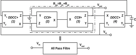
A number of current and voltage mode all-pass filters employing the DDCC have been suggested [17]. How- ever most of these realizations employ floating capacitors and resistors which require a large area to be imple- mented by MOS transistors. The proposed structure use two DDCC, two CCII and only grounded capacitor. The input of the voltage-mode (VM) all-pass filter is con- nected to the Y terminal (high input impedance) and its output is connected to the X terminal (low output im- pedance). For this reason the proposed structure doesn’t necessitate a buffer cascade with another bloc. The ar- chitecture of the filter is given in Figure 1.
The transfer function and the phase of this filter can be expressed by: out in 1 1 eq eq jCR w V V jCR
w (1)
w 2arctg
Req
Cw (2)
The pole frequency of the filter is calculated as: 1 2π o eq f CR
(3)
The type of the filter gives a good solution to realize a controlled Quadrature oscillator [17]. The oscillator fre- quency can be adjusted by means of the value of the ca- pacitor or the bias current of CCII2,3 (the value of Req).
[image:2.595.309.535.83.273.2]However the capacitor values are not variable after inte- gration, for this reason we present an ameliorate structure for the filter when we replaced the grounding capacitor by CMOS Varactors or by a multiplier capacitor [18].
Figure 2 displays the architecture of the ameliorated fil-
ter.
3. The Optimized Differential Difference
Translinear Current Conveyor
The DDCC is a four terminal active block. The symbol and the equivalent circuit of the the DDCC are illustrated in Figure 3.
Vin Vout Y Z X CCII+ (2) Y Z X CCII+ (3)
Y1 Y2
Z XDDCC+ (4) C Y1 Y2 Z X DDCC+ (1)
Vin V
out
Req=Rx1+Rx2
All Pass Filtre
Vin
[image:2.595.59.284.630.721.2]Vout
Figure 1. The proposed all-pass filter.
Y Z X CCII+ (2) Y Z X CCII+ (3) Y
1 Y2
Z XDVCC+ (4) Y1 Y2 Z X DVCC+ (1)
Vin Vout
Vctr
All Pass Filtre
CCMOS
Figure 2. The ameliorated all-pass filter.
Vy1 Vy2 DDCC Y1 Vz Ix Iy2 Iy1 Iz Y2 Z Vx
Figure 3. General representation of DDCC.
The DDCC ensures two functionalities between its te
follower between terminals X and Z. (Y -
r to get ideal transfers, a DDCC should be ch
rminals: A Current
A Voltage follower between terminals X and 1
Y2).
In orde
aracterized by low impedance on terminal X and high impedance on terminals Y1, Y2 and Z. In this configure-
tion, the relation between terminal voltages and currents can be given by the following matrix:
0 1 1 0
V I
1 1
2 2
0 0 0 0
0 0 0 0
1 0 0 0
x X Y Y Y Y Z Z I V I V I V (4)
To realize this structure it’s necessary to cascade C
Voltage Buffer
[3,4]. The input tra
MOS differential voltage buffer (DVB) with a CCII. An implementation of the CMOS differential voltage buffer (DVB) and the CCII are respectively shown in
Figures 4 and 5 [2-4].
A.CMOS Differential
The (DVB) is shown in Figure 4
nsconductance elements are realized with two differ- ential stages (M1 and M2, M3 and M4). The high gain stage is composed of a current mirror (M5 and M6). It converts the differential current to a single-ended output current (M7). The output voltage of this amplifier can be expressed as:
1 1 2 2
x y y y y
V V V (5) where
7 1 6 2 4 6
1
4 5 7 6 7 1 3 5
m m m d d d
Y
m m m m d d d d
g g g g g g
g g g g g g g g
(6)
5 7 2
4 5 7 6 7 1 3 5
m m m
Y
m m m m d d d d
g g g
g g g g g g g g
Vdd
Vss
M5 M6
X'
Y1 Y2
M1M2 M3M4
M10 M7
M9 M8
M11
Figure 4. CMOS differential voltage buffer.
Figure 5. Voltage DC transfer characteristic of the DVB (where Ya = Vx’ and Vy = Vy1 - Vy2).
euristic methodology To determinate the optimal transistor sizes (W and L) or this structure we will use the h
f
[6,7]. This strategy consists on minimizing the imped- ance output value, assuming that the current mirror has unity gain and closer βy1 and βy2 to the unity. The output
resistor is calculated as:
6 1 3 5
4 5 7
m d d d
x
m m m
g g g g
Z
g g g g
m6gd7 gd1gd3gd5 (8)
Simulation conditions are summarized in Ta
the resultant optimal transistor sizes (W and L) se
ble 1 and
are pre- nted in Table 2.
The optimized CMOS differential voltage buffer was simulated with Spice simulation in the ADS software. Main obtained results are represented in Figures 5 and 6. Figure 5 displays the DC transfer characteristics of the
DVB. The voltage transfer can be linear between −0.6 V and 0.6 V. Moreover, the bandwidths of output terminals are shown in Figure 6. The −3dB bandwidths of
1 2
x y y
V V V are located at 3.75 GHz.
The time-domain response of the optimized DVB is shown in Figure 7. A sine wave of 100 mV and −100
mV amplitude and 200 MHz is respectively applied as the input Y1 and Y2 to the filter. We notice that the out-
put Waveforms are confused with the differential input Waveforms Vy1(t) - Vy2(t). This result confirms the good
functionality of this structure.
Figure 6. Frequency response of the voltage follower Vx’/ (Vy1 - Vy2).
Figure 7. The simulation result of voltage waveforms of Vx’ and (Vy1 - Vy2).
logy 0.18 µm CMOS
Table 1. Simulation conditions.
Techno
Supply voltage 1.5 V
Bias current 100 µA
vice sizi
Device Name Aspect ratio W/L (µm)
Table 2. Optimal de ng.
M5-6 13.725/0.18
M1-4 0.25/0.18 M7 7/0.18 M8-11 (current mirrors) 3.05/0.18
B. Transinear Loop Based CCII Configurations
A the second-g translin-
ar loop based current conveyor with a positive current
8 [7]. In T
the translin- ea
4.
with the technol-
n implementation of eneration
e
transfer from X to Z (CCII+) is shown in Figure able 3 we give the different transistor size.
Table 3 shows the optimal device scaling that we get
after applying the optimization approach. The static and dynamic characteristics of r configuration are summarized at Table 4.
Simulation Results of the Proposed
All-Pass Filter
The VM all-pass filter (Figure 1) is simulated
Vdd
Vss
M10 M9 M8 M7
M1 M2
M3 M4
M5 M6
M11 M12
M13
Y X Z
Io
Figure 8. Translinear loop MOS based implementation of CCII.
Table 3. Optimal device sizing.
Device Name Aspect ratio W/L (µm)
M1, M2 6.1/0.18
M3, M4 27.45/0.18
Mxx (in mirrors)
Mxx (in NM nt mirrors)
PMOS current 13.725/0.18
OS curre 3.05/0.18
Tab tics of t CCII
with Io = 100 µA and 1.
Voltage gain β 0.943
le 4. Performance characteris he optimized 5 supply voltage.
Current gain α 1.1
Fci 2.7 GHz
4
Re r 0
Relative Voltage Error
Input Impedance (RY//CY) 1
In ) 24 fF
Fcv .33 GHz
lative current Erro .15%
0.093% 8 KΩ//87 fF
put Impedance (Rz//Cz KΩ//25
Input Resistance Rx 380 Ω
The offset current −2.2 µA
The offset voltage 13 mV
ogy. Th entation of the is shown
in Figu stor aspect ratios S transis-
r were c Tables 2 and 3 he supply
e CMOS implem DDCC+
re 9. The transi
hosen as in
of MO and t to
voltage was ±1.5 V. The biasing current was taken re- spectively as 100 µA for the DDCC and 30 µA for the CCII (Req = RX2 + RX3 = 1.5 KΩ). The simulation results
for the magnitude and phase responses of Vout are shown in Figure 10 where we take C = 6 pF. In this fig-
ure, the pole frequency of 19MHz is obtained. The pole frequency is 19 MHz instead of 17.7 MHz owing to the effect of the parasitic impedances of the DDCC. The relative error between theoretical and simulation value is equal to 7%.
To confirm this result, the circuit is inputted with a si- nusoidal signal of 19 MHz. The input and +90˚ phase shifted output (Vout) are shown in Figure 11. Figure 12
Vss
M5 M6
Y1 Y2
M7 M1M2 M3M4
M11 M9
M8
VDD
M10 I0
M23 M22
Z
M12 M14 M18
M15 M19
M16 M20
M21
M17 M13
Y X
Figure 9. CMOS realization of the DDCC.
Figure 10. Gain and phase responses of proposed all-pass section.
Figure 11. Input and output waveforms for the circuit at 19 MHz.
shows the variability of the pole frequency of Figure 1
lled in the range [11.6 MHz, 36.6 MHz] by vary- g I in the range [10 µA, 200 µA].
first-order all-pass buffer t with the bias current Io2,3. The pole frequency can be
contro in o2,3
5. Quadrature Oscillator Based on the
Proposed All-Pass Filter
To illustrate the utility of the proposed
filter (high input and low output impedances), no is required to connect it to the integrator circui
Vout 2 sRC
[18]), it is connected in cascade toOS DCCIIs, tow CCII
an integrator in a closed loop [17] to construct a quad- rature oscillator, as shown in Figure 13. It is seen that
Figure 12. Pole-frequency tuning with bias current Io2,3.
Vout1
Y
Z X
CCII+
(2) Y
Z
X CCII+
(3) C2
Y1
Y2
Z
X
DVCC+ (1)
Req=Rx1+Rx2
Y1 Y2
Z
X DVCC+
(4)
Y1 Y2
Z X
DVCC+ (5)
C2
Vout2
[image:5.595.125.469.84.274.2]Integrator All Pass Filter
Figure 13. The proposed quadrature oscillator implementation.
equation is given by:
2
1 eq
s s
C R
2 1 2
1 1 2
0 eq
RC C R C R
(9)
This leads to the following oscillation co oscillation frequency respectively:
ndition and
1
1 2
2π
o
eq f
C R C
(10)
2R
2
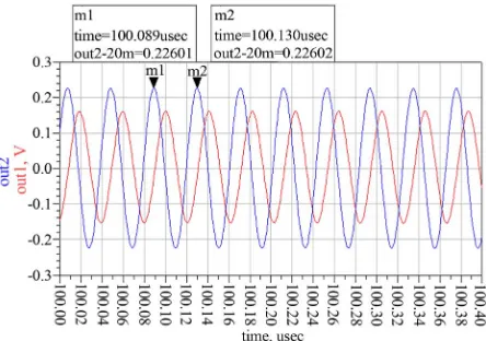
The confirmed performance of the quadrature oscilla- tor can be seen in Figure 14, showin
the oscillator where C = 6 pF, C = 10 pF, R = 600 Ω, an
1
: eq
CO C R C R (11)
g the responses of Figure 14. The simulated quadrature output waveforms of
Vout1 and Vout2.
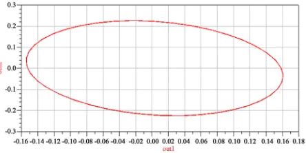
The quadrature relationships between the generated waveforms have been verified using Lissagous figure and shown in Figure 15.
1 2
d Io2,3 = 30 µA (Req = RX2 + RX3 = 1.5 KΩ). The phase
difference between two out puts Vout1 and Vout2 is 90˚ and
[image:5.595.313.535.502.658.2]Figure 15. Lissagous figure.
6. Conclusion
In this paper, we have proposed a new design of VM first-order all-pass filter. In order to get high perform
ances of the fi d CCII struc
tures are optimized in 0.18 µm CMOS process of TSMC. erified with the SPICE simu-
able for VLSI,” IEEE Transac-tions on Circuits and Systems II: Analog and Digital S
nal Processing . 663-670.
http://dx.doi.o
-
lter, a translinear DCCII an -
The theoretical analysis is v
lation program. The application example as the quadra- ture oscillator is included. It shows good usability of the proposed all-pass filter.
REFERENCES
[1] H. Elwan and A. Soliman, “A Novel CMOS Current Conveyor Realization with an Electronically Tunable Current-Mode Filter Suit
ig-, Vol. 43ig-, No. 9ig-, 1996ig-, pp rg/10.1109/82.536763
[2] U. Torteanchai and M. Kumngern, “Current-Tunable Current-Mode All-Pass Section Using DDCC,” Interna-tional Conference on Electronic Devices, Systems and Applications (ICEDSA), Kuala Lumpur, 25-27 April 2011, pp. 217-220.
http://dx.doi.org/10.1109/ICEDSA.2011.5959038 [3] S. Wang and H. Chen, “Tunable Voltage-Mode
Multi-function Biqaudratic Filter with Grounded Capacitors and Resistors Using Two DDCCs,” 3rd International Con-ference on Communication Software and Networks
(ICCSN), 2011.
[4] M. Somdunyakanok, K. Angkeaw and P. Prommee,
“Flo-g Minimum Components,” IEICE
Tran-ating-Capacitance Multiplier based on CCDDCCs and Its Application,” TENCON 2011-2011 IEEE Region 10 Con- ference, pp. 1367-1370.
[5] H. P. Chen and K. H. Wu, “Grounded-Capacitor First- Order Filter Usin
sactions on Fundamentals of Electronics, Communica-tions and Computer Sciences, Vol. E89-A, No. 12, 2006, pp. 3730-3731.
http://dx.doi.org/10.1093/ietfec/e89-a.12.3730
[6] S. B. Salem, M. Fakhfakh, D. S. Masmoudi, M. Loulou, P. Loumeau and N. Masmoudi, “A High Performances CMOS CCII and High Frequency Applications,” Journal
of Analog Integrated Circuits and Signal Processing, Vol. 49, No.1, 2006, pp. 71-78.
http://dx.doi.org/10.1007/s10470-006-8694-4
[7] S. B. Salem, D. S. Masmoudi and M. Loulou, “A Novel CCII-Based Tunable Inductance and High Frequency Current Mode Band Pass Fi
Circuits, Systems, and Computerslter Application,” (JCSC), Vol. 15, No. 6, Journal of 2006, pp. 849-860.
http://dx.doi.org/10.1142/S0218126606003386
[8] A. Bensaied, S. B. Salem and D. S. Masmoudi, “A new CMOS Current Controlled Quadrature Oscillator Based on a MCCII,” Circuit
[9] A. Khan and A. M. T. Ahmed, “Realization o
s and Systems, Vol. 2, No. 4, 2011. f Tunable Floating Resistors,” Electronics Letters, Vol. 22, 1986, pp. 799-800. http://dx.doi.org/10.1049/el:19860548
[10] P. Saaid and A. Fabre, “Class AB Current-Controlled Resistor for High Performance Current-Mode Applica-tions,” Electronics Letters, Vol. 32, 1996, pp. 4-5. http://dx.doi.org/10.1049/el:19960023
[11] R. Senani, A. K. Singh and V. K. Singh, “A New floating Current-Controlled Positive Resistance Using Mixed Translinear Cells,” IEEE Transactions on Circui Systems-II, Vol. 51, 2004, pp. 374-377. ts and http://dx.doi.org/10.1109/TCSII.2004.831381
[12] G. Wilson and P. Chan, “Floating CMOS Resistor,”
Electronics Letters, Vol. 28, 1993, pp. 306-307. http://dx.doi.org/10.1049/el:19930209
[13] V. Riewruja and W. Petchmaneelumka, “Floating Cur-
cations, rentcontrolled Resistance Converters Using OTAs,” In-ternational Journal of Electronics and Communi
Vol. 62, 2008, pp. 725-731.
http://dx.doi.org/10.1016/j.aeue.2007.09.007
[14] M. Kumngern, U. Torteanchai and K. Dejhan, “Voltage- Controlled Floating Resistor Using DDCC,” Radioengi- neering, Vol. 20, No. 1, 2011.
[15] P. Beg, I. A. Khan and M. T. Ahmed, “Tunable Four
ligarh, 14-16 March 2009, Phase Voltage Mode Quadrature Oscillator Using Two CMOS MOCCIIs,” Multimedia, Signal Processing and Communication Technologies, A
pp. 155-157.
http://dx.doi.org/10.1109/MSPCT.2009.5164198
[16] H. O. Elwan and A. M. Soliman, “Low-Voltage Low- Power CMOS Current Conveyors,” IEEE Transaction on Circuits and Sy
tions, Vol. 44, No. 9, 1997.
stems: Fundamental Theory and
Applica-034-010-9150-3
[17] S. Minaei and E. Yuce, “Novel Voltage-Mode All-Pass Filter Based on Using DVCCs,” Circuits, Systems and Signal Processing,Vol. 29, No. 3, 2010, pp. 391-402. http://dx.doi.org/10.1007/s00