Design & Implementation of High Speed Data
Transmission
Umme Habeeba1, S. Rekha2, Dr. A.M Bhavikatti3, Vivekanand M Bonal4
1Fourth Sem M. Tech Appa Institute of Engineering and Technology Karnataka, India 2Asoc. Professor Appa Institute of Engineering and Technology Karnataka, India, rekha_ 3HOD & Professor BKIT Bhalki , 4Head, R&D, Vivek InfoTehch, Kalaburagi, Karnataka.
Abstract:- In this paper, we present a set of data encoding schemes aimed at reducing the power dissipated by the links of an NoC. The proposed schemes are general and transparent with respect to the underlying NoC fabric (i.e., their application does not require any modification of the routers and link architecture). Experiments carried out on both synthetic and real traffic scenarios show the effectiveness of the proposed schemes, which allow to save upto 51% of power dissipation and 14% of energy consumption without any significant performance degradation and with less than 15% area overhead in the NI.
Keywords: Network-On-Chip, FPGA, virtual channel allocation, Switch allocation, Encoder Architecture, power analysis.
I. INTRODUCTION
The diminishing semiconductor transistor dimensions make it possible to integrate more Intellectual Property (IP) blocks in a single System-on-Chip (SoC). However, this poses fresh problems in inter-IP connectivity. Conventional shared bus interconnection lacks flexibility and scalability in dealing with a large number of IPs in a single chip. To ease these limitations, network-on-chip (NoC) has been introduced [1]. For maintaining good throughput, a router needs to perform NoC separates the computation from the communication several stages such as route computation, VC allocation, and parts, while providing a scalable and flexible modular design.
Switch allocation in parallel. In order to reduce on-chip memory usage, wormhole flow NoC router is still a challenge for on-chip systems [7].In order to reduce the communication latency while maintaining good throughput, a router needs to performs everal stages such as route computation, VC allocation, and switch allocation in parallel. However, designing a low latency NoC router is still a challenge for on-chip systems [7]. In this work, a microarchitecture for a low latency NoC router is proposed. The advantages of existing related works such as look-ahead routing computation [2, 3],combination of VC/SW allocation [4, 5], and replacing VC allocator with a queue of free VCs [3, 6] are used. Meanwhile, several optimization techniques such as efficient masking of the allocation requests and broadcasting only two status bits instead of using proxy credit register have been applied to provide high operating frequency, reasonable hardware cost, and high utilization of the available buffer space.
II. RELATED WORK
To purge the need for a separate pipeline stage for routing computation, look-ahead routing was proposed [12]. In the look-ahead routing, the output port is computed one router in advance and is attached to the header flit. Hence, at the header flit arrival time, the NoC router can start the sending of the allocation request to the precomputed output port while computing the next router output port in parallel. To remove the dependency between VC allocation and switch allocation, speculative switch allocator was proposed . In speculative allocation, a header flit is acceptable to send requests to both switch and VC allocators in parallel by speculating that an OVC will be assigned successfully. However, in the case when the VC allocation is unsuccessful, the granted switch allocation is ignored. Since ignoring a granted request results in an unused time slot, the NoC sets a higher priority to the switch allocation requests that have already been assigned OVCs (non speculative requests) to the ones that have not been assigned any OVC. The speculative allocation performs well when the router carries light traffic. However, in dealing with heavy traffic, it becomes inefficient due to the increase in unsuccessful speculations.
III. PROPOSED NOC ROUTER
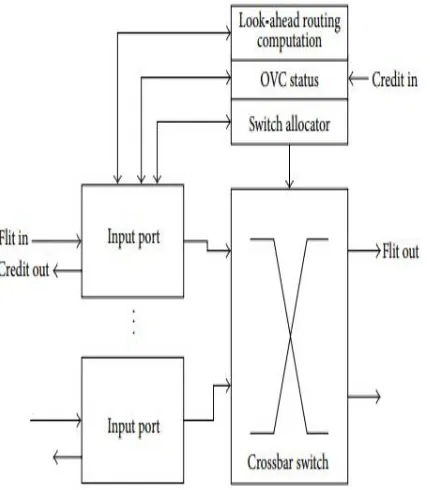
[image:3.612.207.422.196.441.2]In this paper , a two-clock-cycle latency router microarchitecture with parallel VC and switch allocator is used. Our proposed architecture eliminates the necessity of setting higher priority to any IVC requests. In the proposed NoC router architecture, any request which has been granted service by the switch allocator is able to pass a flit to the output port successfully. An well organized masking technique is proposed to sort all switch allocation requests that are not able to pass flits to the output port, either due to the lack of free space in assigned VC or due to the lack of free VC in the output port for non assigned VC requests. The masking technique also provides an efficient usage of VC memory buffers. Our proposed design has least impact in timing and area overhead of an NoC router. It is also fully parameterizable in terms of number of VCs, buffer width, and flit width.
Figure 1: Block diagram of the proposed NoC router.Figure 1 shows the block diagram of the proposed NoC router architecture. It consists of the following components;
A. Input Switches
In input port module is first to receive the data packet flits. After receiving a flit, the VC-ID of each flit is examined in order to allocate it into the respective VC FIFO buffer.
B. Look-Ahead Routing Computation Module
Look-ahead routing is applied in order to relax the dependencies of the first stage of conventional router, which is the route computation. Conventional VC allocator has two main drawbacks in terms of circuit complexity and high critical path delay
C. Ovc Status Modul
Using a conventional VC allocator, it is possible to allocate multiple OVCs inside the same output port in one clock cycle. However, in any clock cycle, only one flit can be passed to an output. Hence, multiple simultaneous OVC allocations will give no significant improvement in performance. A speculative NoC with canonical VC allocator may outperform a speculative NoC using queues of VCs in term sof performance, as simultaneous multiple VC allocations on one port reduce the number of speculative requests and thereby, speculation failure.
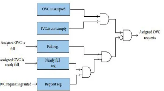
defined as an OVC which has not been assigned and has at least one available credit. In our approach, we propose a feedback of only two fixed status bits for each IVC. These two bits determine the condition of assigned OVCs which are full and nearly full (i.e., has only one empty place).
Figure 2: The status signals transferring from OVCs to an IVC
Figure 2 shows the architecture for transferring the assigned OVC status to an IVC. It consists of two levels of multiplexing, where the first level selects all OVC status inside the output port and the second level returns the assigned OVC status bits. This structure is repeated for each respective IVC. The status bits are registered at the input ports in order not to add the multiplexing time to the router critical path. The one clock-cycle delay in receiving status bit will be handled by the masking filter inside each input port. To this end, the granted IVC request that is delivered to each input port at the end of allocation stage is stored in a register. Hence, this register indicates the condition of IVC request in the last clock cycle.
1) Now, each IVC masks the requests if
a) The status registers show the full status for the assigned OVC and
b) An assigned OVC status register is nearly full and the request status register indicates that the previous IVC request has been granted by the allocator.
[image:4.612.180.460.422.578.2]In the second condition, when the last request is granted, the real OVC status is full but will be updated in the next clock cycle. The masking filter is shown in Figure 3.
Figure 3: The assigned OVC requests masking
D. SW allocator module
Figure 4: The switch allocator functional block diagram
IV. ENCODING ARCHITECTURE SCHEMES
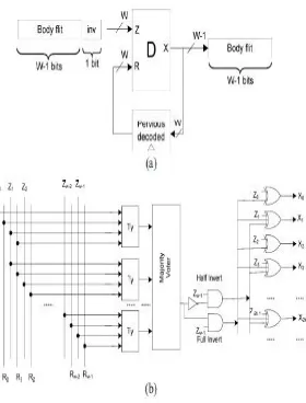
A. Scheme-i
The main purpose of proposed encoder design is secured data transmission in noc while keeping considerations of reducing power, area, delay both on software and hardware(FPGA).
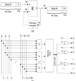
Figure 5: Encoder architecture Scheme-I:a)circuit diagram b)internal view of encoder block (E).
In the scheme 1 we have encoder E ,which is used to find the number of transitions. i.e bits changed from 1-0 or 0-1. EX:16 Bit data,1000001100110011. for finding the transitions in above data stream without encoder above it will consume more power. By using above scheme we only see the transitions which changing its state from 1-0 or 0-1 there are 6 transitions for given bit stream. To make the decision, the previously encoded flit is compared with the current flit being transmitted. This latter, whose w bits are the concatenation of w − 1 payload bits and a “0” bit, represents the first input of the encoder, while the previous encoded flit represents the second input of the encoder.
B. Scheme-Ii
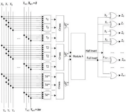
Figure 6: Encoder architecture Scheme-II
In scheme II there are T2,T4 blocks are present and Ty blocks are also present. In T2 block the number of maximum transitions are 2.In T4 block the number of maximum transitions will be 4.The scheme compares the current data with the previous one to decide whether the odd, full, or no inversion of the current data can give rise to the link power reduction. To check the Ty is odd invert or even invert, we have
(1)
Where W=size of input data the condition used to determine whether the odd inversion has to be performed or not. The second stage of the encoder, which is a majority voter block, determines if the condition given in eqn(1) is satisfied (a higher number of 1s in the input of the block compared to 0s). If this condition is satisfied, in the last stage, the inversion is performed on odd bits. The decoder circuit simply inverts the received flit when the inversion bit is high.
C. Scheme-Iii
Figure 7: Encoder architecture Scheme-III
[image:6.612.200.416.513.687.2]which is based on the even invert condition of (8),the full invert condition of (9), and the odd invert condition of (10), is shown in Fig. 6. we have four Ones blocks to determine the number of detected transitions for each Ty, Te, T2, T 4 , blocks. The output of the Ones blocks are inputs for Module C the operation of module C is based on counter. This module determines if odd, even, full, or no invert action corresponding to the outputs “10,”“01,” “11,” or “00,” respectively, should be performed. The outputs “01,” “11,” and “10” show that whether (8), (9),and (10), respectively, are satisfied. In this paper, Module C was designed based on the conditions given in (8), (9),and (10). Similar to the procedure used to design the decoder for scheme II, the decoder for scheme III may be designed.
[image:7.612.166.446.200.568.2]D. Scheme-II Decoder architecture
Figure 8: Decoder architecture Scheme-II
For the decoder, we only need to the Ty block to determine which action has been taken place in the encoder. Based on the outputs of these blocks, the majority voter block checks the validity of the inequality given by (1). If the output is “0” (“1”) and the inv = 1, it means that half (full) inversion of the bits has been performed. Using this output and the logical gates, the inversion action is determined. If two inversion bits were used, the overhead of the decoder hardware could be substantially reduced.
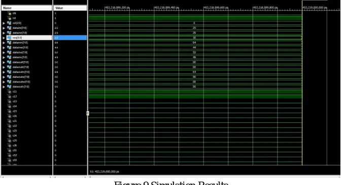
V. RESULTS AND DISSCUSSIONS
Figure 9 Simulation Results
The encoder schemeIII with NoC switch is used for high security, the encoder is used at the transmitter and decoder is used at receiver .The encoder output is the input to the decoder, the decoder is correct bits which are corrupted while transmitting through noisy channel and any media it uses xor operation for transimission of bits.
VI. CONCLUSION
The results are given by analysing different schemes of encoders for NoC. The proposed router micro architecture is optimized in three main criteria, which are area, minimum power dissipation ,and delay compared to existing works. The proposed typical NoC is simulated in XILINX 14.7 with Verilog HDL. The proposed NoC router has been implemented on Virtex-5 FPGA using Chip scope pro by itegrated logic analyzer (ILA) and integrated controller (ICON).
REFERENCES
[1]. W. Dally and B. Towles, “Route packets, not wires: on-chip interconnection networks,” in Proceedings of the Design Automation Conference, pp. 684–689,
2001.
[2]. R.Mullins, A.West, and S.Moore, “The design and implementation of a low-latency on-chip network,” in Proceedings of the Asia and South Pacific Design
Automation Conference, pp. 164– 169, January 2006.
[3]. D. U. Becker, Efficient microarchitecture for network-on-chip routers [Ph.D. thesis], Stanford University, Stanford, Calif, USA,2012.
[4]. S. T. Nguyen and S. Oyanagi, “The design of on-the-fly virtual channel allocation for low cost high performance on-chip routers,” in Proceedings of the 1st
International Conference on Networking and Computing (ICNC ’10), pp. 88–94, IEEE, November 2010.
[5]. Y. Lu, J. McCanny, and S. Sezer, “Exploring virtual-channel architecture in FPGA based networks-on-chip,” in Proceedings of the 24th IEEE International
System on Chip Conference (SOCC’11), pp. 302–307, September 2011.
[6]. R. Mullins, A. West, and S. Moore, “Low-latency virtual channel routers for on-chip networks,” in Proceedings of the 31st Annual International Symposium on