2018 International Conference on Computer, Electronic Information and Communications (CEIC 2018) ISBN: 978-1-60595-557-5
Multi-mode High-efficiency PWM AC/DC Controller Design
Min QI
1,2, Quan SUN
3,*and Dong-hai QIAO
11
Institute of Acoustics, Chinese Academy of Sciences, Beijing, 100190, China 2
University of Chinese Academy of Sciences, Beijing, 100049, China 3
Southern Methodist University, Dallas, TX, 75206, USA
*Corresponding author
Keywords: PWM, AC/DC, Controller, Logic controller, Multi-mode, Energy Star VI.
Abstract. This paper proposes a multi-mode pulse-width modulation (PWM) AC/DC controller, which was implemented on a 40-V 0.8-µm one-poly two-metal (1P2M) CMOS process. It can change the operation mode by using an inner logic controller to improve the conversion efficiency under all load conditions. The necessary protection circuits are integrated on chip to reduce the number and size of the discrete components. The area of the chip is as small as 1410 X 730 um2. The standby power is lower than 100mW, and the conversion efficiency is higher than 85%. Test results have met the most stringent power consumption standards of “Energy Star VI”. The Design has achieved the industrial mass production, used in portable electronic device adapter.
Introduction
Power supply is the power support of the electronic equipment in modern communication, aerospace, biotechnology and other high-tech fields. Switching power supply and linear power supply are the two main technologies of the modern electronic power supply, in which the switching power supply is characterized by lower power consumption, higher efficiency, smaller volume and lighter weight, etc. The average efficiency of the PWM switching power supply is usually up to 65~70%. However, with the increasingly market demand of the portable electronic devices, 70% conversion efficiency is not enough. In July 2013, the Department of Energy (DoE) pushed "the requirements of external power adaptors" to "Energy Star VI standards", as shown in table 1.
Table 1. DoE Level VI.
Average efficiency Standby power [mW]
≥ 85.00% < 100
This work recommends a high-performance PWM AC/DC controller using multi-mode quasi-resonant technology according to the Energy Star VI standard, which is implemented on a 40-V 0.8-µm 1P2M CMOS process [1]. It has been proved that the chip is smaller and costs lower than the mainstream products at home and abroad. Moreover, this design has been mass produced on an industrial scale utilized in power adapters of portable electronic devices.
In Section 1, the proposed high-efficiency AC/DC voltage controller is illustrated. Section 2 introduces the test results obtained for the overall chip, while Section 3 concludes by explaining how the application of the proposed AC/DC controller meets the Energy Star VI standard.
Controller Chip Design
Key Technologies of High-efficiency Switching Power Supply
widely used control mode. The traditional PWM is composed of reference voltage, comparator, error amplifier, oscillator and other modules, and is also the foundation of the AC/DC controller. The in-depth theory can be referred in reference [2].
There are three points about the key technologies of high-efficiency PWM AC/DC voltage controller. The first is to use the logic controller to control the working mode of PWM modulation under different loads, which can overcome the disadvantages of low efficiency of PWM in light load or no-load. Secondly, the switching loss of switching power supply is reduced by using the quasi-resonant technology. Thirdly, under high supply voltage, the working voltage of core circuit is reduced by the built-in low dropout (LDO), which reduces the power consumption of the entire system to a great extent. This paper introduces the first point in this design.
The common working modes are named as continuous current mode (CCM), discontinuous current mode (DCM), critical conduction mode (CRM) and Burst [3]. Under full load, PWM modulator usually works in CCM mode which is the optimization one due to the lower noise and higher efficiency. On the contrary, under light load or no load, if the switch operating frequency is changeless, the switching loss will be accounted for most of the system power consumption, resulting in lower system efficiency. The multi-mode modulating adopted in this design is a commendable method to solve this problem. The circuit can follow the load variation and adjust the working mode, which has a great relationship with the switching frequency. Multi-mode modulation greatly improves the efficiency under all kinds of load conditions.
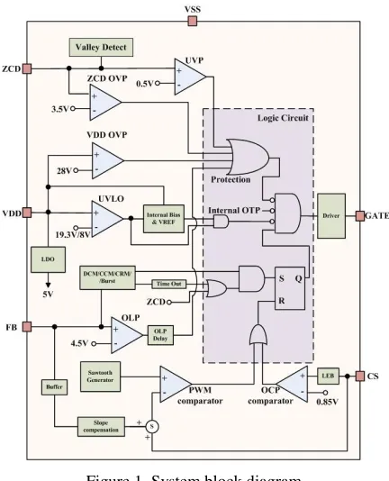
[image:2.612.197.413.355.622.2]Overview of the Chip Structure
Figure 1. System block diagram.
relationships are simply illustrated in figure 1. All kinds of these protections are used to prevent the circuit from being damaged due to the abnormal conditions. In addition, an on-chip 5-V low dropout (LDO), which powers the major blocks of the AC/DC controller, is also integrated. Furthermore, it has been proven that the controller is an ideal design for low-cost applications.
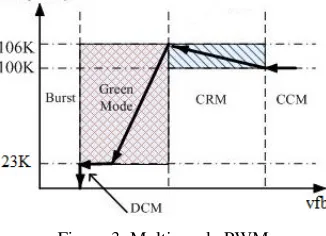
[image:3.612.166.448.154.321.2]Multi-mode PWM Modulation
Figure 2. Flyback topology.
Figure 2 is the recommended flyback topology circuit, which is the application circuit designed for system simulation and testing [6]. The multi-mode quasi-resonant PWM AC/DC conversion introduced in this paper can be perfectly implemented through this topology.
[image:3.612.223.386.461.579.2]In figure 2, U1 is the integrated circuit (IC) we designed which is used to drive the power MOSFET M1. There are also several precise references voltages produced in U1.The feedback voltage vfb is affected by the change of the load current through an optocoupler U2. Comparing the vfb and these references step by step, the inner logical controller adjusts the duty ratio of the output GATE to accommodate the load current. The inner logic controller changes the working mode according to the switching frequency and vfb voltage.
Figure 3. Multi-mode PWM.
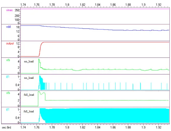
Figure 4. Simulation at no-load condition and full-load condition.
Chip Layout
[image:4.612.214.399.357.467.2]The design implemented on a 40-V 0.8-µm 1P2M CMOS process. The chip area only occupies 1410 X 730 um2, and the micrograph is in figure 5.
Figure 5. Chip micrograph.
Test Results
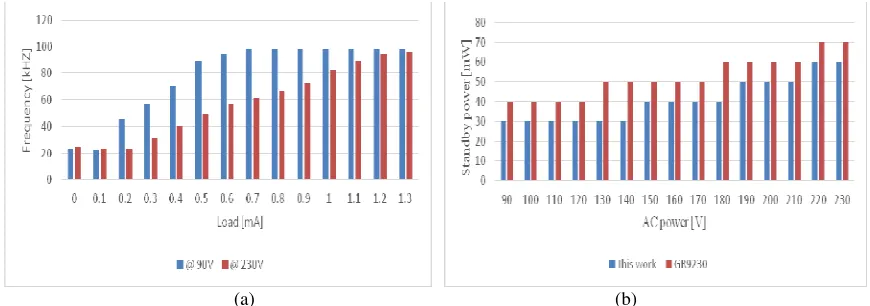
Figure 6 (a) demonstrates the relationship between the switching frequency and the load current. When the AC supply is fixed, the variation trend of switching frequency is as same as that of the load current. At light-load conditions, the lower switching frequency can save power effectively.
(a) (b)
Figure 6. (a) Frequency vs. Load. (2) Standby power vs. AC supply.
Conclusion
In this paper, a multi-mode high-performance PWM AC/DC controller is presented, which can drive a 650-V power MOSFET according to the Energy Star VI standard in typical applications of AC/DC adapters in portable electronic devices. This work is based on a 40-V 0.8-µm 1P2M CMOS
technology. The chip area only occupies 1410x730 µm2. The standby power is lower than 100mW and the conversion efficiency is higher than 85%. Furthermore, the controller can be applied in quick-charge applications, which are the most advanced power adapters in the market. The controller has been mass produced on an industrial scale.
Acknowledgement
This research was financially supported by the National Science and Technology Major Project.
References
[1] Yong Li, Jerry Zheng. A low-cost adaptive multi-mode digital control solution maximizing AC/DC power supply efficiency. Twenty-Fifth Annual IEEE Applied Power Electronics Conference and Exposition (APEC), 2010: 349-354.
[2] Seok-Kyoon Kim, Jung-Su Kim, Young Il Lee. A simple model predictive controller of a three-phase PWM AC/DC converter. International Conference on Control, Automation and Systems (ICCAS), 2013: 1571-1576.
[3] G. Rakesh, Naran M. Pindoriya. Simulation and experimental study of single phase PWM AC/DC converter for Microgrid application. IEEE 1st International Conference on Power Electronics, Intelligent Control and Energy Systems (ICPEICES), 2016: 1-6.
[4] Pan Hong, Wu Xiaobo, Chen Hai, et al. Power supply module design in the low power consumption application. IEEE Conference on Electron Devices and Solid-State Circuits, 2007: 401-404.
[5] Min-Hyeong Cho, Won-Ho Lee, Jin-Su Kim, et al. Development of undervoltage lockout (UVLO) circuit configurated Schmitt trigger. International SoC Design Conference (ISOCC), 2015: 59-60.
[image:5.612.88.523.66.219.2]