2018 International Conference on Applied Mechanics, Mathematics, Modeling and Simulation (AMMMS 2018) ISBN: 978-1-60595-589-6
Performance Analysis of a PWM DC–DC Converter for PEMFC Stack
Power Conditioning Applications
Makani MWINGA, Ben GROENEWALD
*and Michael MCPHERSON
Cape Peninsula University of Technology, Cape Town, South Africa *Corresponding author
Keywords: PEMFC, Voltage balancing, Interleaving, Power conditioning, DC – DC converters.
Abstract. A Fuel cell stack inherently generates low unregulated voltage, which is not useful for most power supply applications. In order to make this voltage useful, often a power conditioning system that consists of a converter or inverter or a combination of both is connected intermediate to the fuel stack. Several topologies for converters and inverters exist. In this paper, the performance of a transformerless pulse width modulated dc–dc interleaved boost voltage multiplier converter with current ripple reduction capability is analyzed for PEMFC stack power conditioning applications. Key experimental results are included, which indicate that the stack output voltage was regulated and boosted, and highlight the voltage balancing challenge arising from interleaving.
Introduction
Fuel cells (FCs) are considered to be among one of the better renewable energy generating sources [1]–[8]. Several types of fuel cells exist [9]–[11]. These can be classified according to the membrane used, the fuel requirements and the operating temperature range requirements[12]–[15]. FCs inherently produce low voltage, are susceptible to high current ripple and have slow dynamics [9]–[11], [16], [17]. Therefore, for practical power supply applications, the individual FCs are connected together to form a FC stack, which produces a higher voltage compared to that of individual FCs [16], [18]. However, the resulting FC stack voltage is unregulated and of small magnitude for most practical power supply voltage requirements [19]. In order to overcome the limitations of the generated FC stack voltage, a power conditioning system (PCS) is necessary [20], [21]. Often, a PCS is connected intermediate the FC stack and the load. The function of the PCS is to regulate and boost the FC stack voltage to a high voltage level, corresponding to that of the voltage specification of the load.
(a) (b) Load high Vdc Fuel Cell stack PWM Controller dc-dc converter Filtering elements Load high Vdc Fuel Cell stack PWM Controller dc-dc converter Filtering elements
Figure 1. Fuel cell power conditioning systems: (a) Voltage source dc–dc converter topology. (b) Current source dc – dc converter topology.
Converter Topology
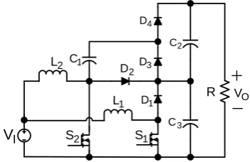
Fig. 2 shows the circuit of the interleaved boost voltage multiplier converter. The circuit topology is derived from the work of [39], [40]. The operation and mathematical modelling of converter is discussed in [41]. The converter comprises of two boost converters interleaved together with a diode–capacitor combination feature as the voltage multiplier. Under steady state analysis and considering continuous current condition mode (CCM) operation, the system exhibits two distinct voltage and current switching waveforms over one switching cycle. Where, one particular set of voltage and current switching waveforms is obtained for duty cycle values less than 0.5 and another for duty cycle values greater than 0.5. Details of the switching waveforms and dynamic equations thereof are given in [19].
The paralleling of inductors at the front end facilitates current ripple cancellation, and the diode– capacitor combination facilitates further voltage boosting. Ideally, this configuration should permit a reduction in the stack current ripple, while at the same time ensuring high voltage boosting without use of a transformer.
I
V S2
1 L D1
2 C R 1 C 2 L 1 S 2 D D3
[image:2.595.209.385.422.536.2]3 C 4 D O V
Figure 2. Interleaved boost voltage multiplier converter.
Experimental Results and Discussion
Experimental Setup
Fig. 3 shows the experimental setup for the IBVM converter prototype circuit. The setup consists of a dual dc power supply, 1 kW PEMFC stack and stack controller, DMM, variable electronic load, 100 MHz digital LeCroy oscilloscope, hydrogen gas supply pipe and the IBVM converter prototype circuit.
DMM 1 kW PEMFC stack Variable electronic load 100 MHz LeCroy digital oscilloscope Hydrogen gas supply pipe Laptop
Dual variable DC power supply
1 kW PEMFC stack controller
[image:3.595.167.428.73.253.2]IBVM converter prototype circuit
Figure 3. Experimental setup for the IBVM converter prototype circuit.
[image:3.595.71.527.350.480.2]IBVM Converter Prototype Circuit
Table I shows the design specifications which were adopted for the design and development of the IBVM converter prototype Circuit.
TABLE I. Design Specifications of Converter Prototype Circuit.
Parameter Value Comments
O
P 0 – 900 W 0 – 30 W nominal output power
I
V 36 – 67 V dc 58 V dc nominal input voltage
O
V 200 V dc nominal converter output voltage
0.9 efficiency at full-load
I
I 0.3 of IL Input current ripple
O
v
0.3of VO Output voltage ripple
S
f 50kHz Switching frequency
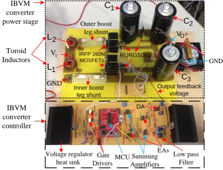
Fig. 4 shows the IBVM converter prototype circuit and controller. The circuit comprises of the input voltage terminals VI , two toroid input inductors L1 and L2, an outer and inner boost leg shunt,
two IRFP260N power MOSFETs, two TLP251 gate drivers, four RURG5060 ultrafast diodes, a controller and three aluminium electrolytic capacitors: C1, C2 and C3. The PEMFC stack voltage is
coupled to the IBVM converter prototype circuit via the converter input voltage terminal. The converter boosts and regulates the stack voltage to a high converter output voltage of about 200 V dc. Toroid Inductors 1 L 2 L I V GND 2 C 1 C 3 C IRFP 260N MOSFETs Outer boost leg shunt Inner boost leg shunt IBVM converter controller Voltage regulator
heat sink MCU
Gate Drivers EAs Summing Amplifiers Low pass Filter DA RURG5060 Output feedback voltage O V GND IBVM converter power stage
[image:3.595.184.409.587.758.2]An MSP430G2553 low cost and low power mixed signal microcontroller unit (MCU) was utilized for PWM control. The MSP430G2553 has several pinouts and programmable peripherals. The MCU generated two PWM gate signals required for switching of the converter MOSFET switches. Key MCU peripherals utilized for the converter controller application include input/output (I/O) pins, system clock, timers, ADC10 module and CPU. A comprehensive description of the device features can be found in the device data sheet.
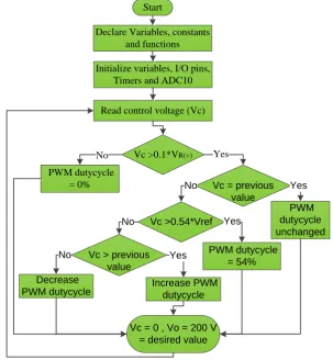
Fig. 5 shows the key program algorithm adopted in the development of the software program for the generation of two PWM gate signals, using the MSP430G2553 MCU. First, the MCU is powered up at start-up; then the variables, constants and functions are declared; followed by the initialization of variables, I/O pins, functions, timers and ADC10 module. Once the initialization process is complete, the ADC10 module continuously samples the analog feedback voltage via the MCU analogue input pins. The sampled analogue voltage is then converted into digital format.
Vc >0.1*VR(+)
Start
No
Vc >0.54*Vref
Yes
PWM dutycycle = 0%
Declare Variables, constants and functions
Initialize variables, I/O pins, Timers and ADC10
Read control voltage (Vc)
Vc = previous value
PWM dutycycle unchanged
Yes No
Decrease PWM dutycycle
No
PWM dutycycle = 54% Yes
Vc > previous value No
Increase PWM dutycycle
Yes
[image:4.595.145.449.246.575.2]Vc = 0 , Vo = 200 V = desired value
Figure 5. Key program algorithm steps adopted for C code program write–up required for generation of two PWM gate signals using an MSP430G2553 MCU.
Special functions registers were used in order to configured and initialize I/O pins, timers, ADC10 module and other required peripherals.
Timer0_A3 and Timer1_A3 were configured to operate at a fixed switching frequency of 50 kHz as up/down counters. Timer1_A3 counter was programmed to have a count delay of 180o phase from that of Timer0_A3, in order to warrant a 180o phase shift between the two generated PWM gate signals.
NADC = 1023[(VC – VR(–))/ (VR(+) – VR(–))] (1)
Where NADC in Eq. 1 is the decimal value of the analogue-to-digital conversion of the ADC10 module, VR(–) and VR(+) are the negative and positive reference voltages of the ADC10 module. For
our application, VR(+) and VR(–) were set to 2.5 V and 0 V respectively.
The ADC10 module continually samples the analogue control voltage, VC, and simultaneously
performs analogue-to-digital conversion of the sampled analogue voltage. By default, the ADC10 conversion results are stored in the ADC10MEM register. Another option is to store them in global variables, for ease manipulation of the data. For our application, two global variables, ADCRead and ADCRead1 were selected. Timer0_A3 and Timer1_A3 use the values in the global variables to adjust the duty cycle of the generated pulse width modulated (PWM) gate signals. The duty cycle is proportional to the ratio of control voltage to positive reference voltage. Once the duty cycle of the gate signals is changed, the program loops back to the sampling phase of the analogue control voltage, then MCU updates the global variables and the process repeat indefinitely.
Experimental Results
The experimental results of the IBVM converter prototype circuit and the PEMFC stack are discussed in this section. A 100MHz LeCroy oscilloscope with a sampling rate of 1 GS/s was used to capture the experimental measurements. The following experimental measurements were obtained: gate-to-source and drain-to-source voltages of the MOSFETs, inductors current ripples, capacitor voltage, PEMFC stack output voltage and IBVM converter output voltage.
A 350 W variable electronic load was utilized as the load for the converter. Due to limitations in the power handling capability of the prototype circuit, the load was varied over a range of 0 W to 30 W, in increments of 20 W and 10 W.
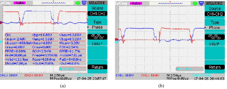
Fig. 6 (a) shows the gate-to-source voltage waveforms of the MOSFETs at 20 W of power–load. The waveform shown at CH1 corresponds to the voltage across the gate and source of the inner boost leg MOSFET. On the other hand, the waveform shown at CH2 corresponds to the voltage across the gate and source of the outer boost leg MOSFET. The results indicate that the voltage across the gate-to-source terminal of the MOSFETs has a frequency of 49.99 kHz, amplitude of 13.6 V, 39 % duty cycle, 188.1o phase shift and a period of 20 µs.
Fig. 6 (b) shows the gate-to-source voltage waveforms of the MOSFETs at 30 W of power–load. The inner boost leg MOSFET has a mean of 7.60 V, amplitude of 13.6 V, peak–to–peak of 18 V and maximum of 14 V. On the other hand, the outer boost leg MOSFET has a mean of 7.20 V, amplitude of 13.2 V, peak–to–peak of 19.2 V and maximum of 14.8 V.
(a) (b)
Figure 6. (a) The gate–to–source voltage waveforms of the MOSFETs at 20 W of power–load. (b) The gate–to–source voltage waveforms of the MOSFETs at 30 W power–load.
[image:5.595.71.530.531.711.2]maximum of 278 V. On the other hand, the outer boost leg MOSFET has a mean of 56 V, peak to peak of 126 V, amplitude of 110 V and maximum of 118 V. The results indicate that the voltage measurements for the inner boost leg MOSFET are greater than those for the outer boost leg MOSFET. Results also show that the inner boost leg MOSFET voltage has oscillations before turn off, while that of the outer boost leg has smooth turn on and turn off transitions.
Fig. 7 (b) Shows the drain-to-source voltage waveforms of the MOSFETs at 30 W of power–load. The inner boost leg MOSFET retains oscillates before turn off, has a mean of 64 V and all other measurements stay the same. On the other hand, the outer boost leg MOSFET retains smooth turn on and turn off transitions, has a mean of 60 V, peak–to–peak of 128 V, amplitude of 112V and maximum of 120 V.
Fig. 7 (c) and (d) show the voltage waveform corresponding to the inductors current ripples. The waveforms indicate that the inductor current ripples are out of phase. LTSR 25–NP current sensors were used to measure the current. An LTSR 25–NP sensor outputs a voltage proportional to the current flowing through it. The current measured by the sensor is given by Eq. 2. Where Vsensor is the
sensor voltage corresponding to the sensed current, VR is the reference voltage for the sensor
specified as 2.5 V and Imax is the maximum current rating of the sensor specified as 25 A.
I = (Vsensor / VR)Imax (2) The voltage measurements for the inductors current ripples are given as 68 mV for L1 and 40 mV
for L2. Substituting these values in Eq. 2, the inductors current ripples were calculated and they are
given as 0.68 A and 0.4 A.
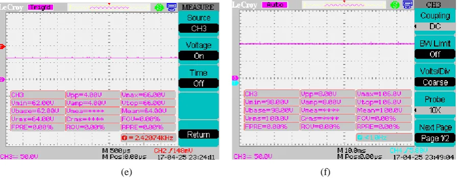
Fig. 7 (e) shows the measurements of the PEMFC stack voltage waveform for open circuit (no– load) condition. The open circuit voltage of the stack has a maximum voltage of 66 V, which is approximately equal to the rated stack open circuit voltage of 67 V.
Fig. 7 (f) shows voltage measurements of the voltage across C3 at 20 W of power–load. The
voltage across C3 has a peak–to–peak of 8 V and a mean of 204 V. The measured voltages across all
capacitors are approximately equal; thus the converter output voltage is approximately twice the voltage across C3. This validates the voltage balancing feature analysis of the IBVM converter
discussed previously.
(a) (b)
[image:6.595.108.490.471.777.2]
(e) (f)
Figure 7. (a) The drain-to-source voltage of the MOSFETs at 20 W of power–load. (b) The drain–to–source voltage of the MOSFETs at 30 W of power–load. (c) The voltage waveform corresponding to the inductor current ripple of L1.
(d) The voltage waveform corresponding to the inductor current ripple of L2. (e) The open–circuit voltage waveform and voltage measurements for the PEMFC stack. (f) The voltage waveform and voltage
measurements across C3 at 20 W power–load.
Fig. 8 (a) shows voltage measurements of the converter output voltage. The converter output voltage has a peak–to–peak of 12 V, a mean of 204 V. Fig. 8 (b) shows the converter and PEMFC stack output voltage waveforms and converter voltage measurements at 30 W of power–load. The converter output voltage measured at CH3 has a peak–to–peak voltage of 20 V, a mean of 204 V and maximum of 218 V. On the other hand, the PEMFC stack voltage measured at CH4 has a peak–to– peak voltage of 26 V and a mean of 56 V.
(a) (b)
Figure 8. (a) The converter output voltage waveform and voltage measurements at 20 W power–load. (b) The converter and PEMFC stack output voltage waveforms at 30 W of power–load.
Conclusion
The focus of this paper was on the performance analysis of a dc–dc IBVM converter prototype circuit for PEMFC stack power applications. Specific experimental measurements were carried out to evaluate the performance of the system. Due to limitations in the power handling capability of the PCB, the maximum power of the system was restricted to 30 W instead of 1 kW.
[image:7.595.76.525.72.247.2] [image:7.595.71.526.408.593.2]shifted, therefore warranting ripple cancellation and thereby facilitating a reduction in the stack output ripple.
The results reveal a disparity between the drain-to-source voltages of the MOSFETs, with voltage oscillations and high power dissipation occurring across the inner boost leg MOSFET. The disparity in the voltage measurements can be attributed to the imbalance resulting from the voltage sharing between the inner and outer boost legs of the converter. This imbalance also leads to high power dissipation across the inner boost leg MOSFET. On the other hand, the voltage oscillations can be attributed to the parasitic elements and presence of a high drain-to-source voltage across the inner boost leg MOSFET. Effects of the voltage oscillations include reduced on-time duty cycle induced by early turn off transitions.
Implementation of converter interleaving needs to consider better solutions that can eliminate or reduce to a negligible value the imbalance in the voltage sharing between interleaved converter legs and the disparity between the drain–to–source voltages of the MOSFETs.
Acknowledgment
The author would like to thank HySA systems centre at the University of the Western Cape, South Africa, for the permission to use their lab facility during the experimentation phase of the converter prototype circuit.
Further thanks goes to my supervisors for their contribution towards the work presented herein.
References
[1]L. Zhao et al, “Fuel Cells for Data Centers : Power Generation Inches from the Server,” J. Power Sources, 2014.
[2]J. M. Corrêa, F. A. Farret, L. N. Canha, and M. G. Simoes, An electrochemical-based fuel-cell model suitable for electrical engineering automation approach, IEEE Trans. Ind. Electron., 2004. [3]C. Li, R. Zhou, and T. Li, Enabling distributed generation powered sustainable high-performance data center, HPCA, 2013.
[4]W. Katsak, K. Le, T. D. Nguyen, R. Bianchini, and Í. Goiri, Parasol and GreenSwitch: Managing Datacenters Powered by Renewable Energy, SIGARCH Comput. Arch. News, 2013. [5]Y. Li et al, SizeCap: Efficiently handling power surges in fuel cell powered data centers, HPCA, 2016.
[6]S. Yu, T. Fernando, T. K. Chau, and H. H.-C. Iu, Voltage Control Strategies for Solid Oxide Fuel Cell Energy System Connected to Complex Power Grids Using Dynamic State Estimation and STATCOM, IEEE Trans. Power Syst., 2017.
[7]L. Zhao et al, Fuel Cell Powered Data Centers: In-Rack DC Generation, ECS Trans., 2016. [8]J. Brouwer, S. James, and E. Peterson, Servers Powered By a 10kW In-rack Proton Exchange Membrane Fuel Cell System, Proc. Int. Conf. Energy Sustain. 2014.
[9]A. Kirubakaran, S. Jain, and R. K. Nema, A review on fuel cell technologies and power electronic interface, Renew. Sustain. Energy Rev.13 (2009) 2430–2440.
[10]F. Mueller, F. Jabbari, R. Gaynor, and J. Brouwer, Novel solid oxide fuel cell system controller for rapid load following, J. Power Sources, 2007.
[11]F. Mueller, F. Jabbari, and J. Brouwer, On the intrinsic transient capability and limitations of solid oxide fuel cell systems, J. Power Sources, 2009.
[13]O. Z. Sharaf and M. F. Orhan, An overview of fuel cell technology: Fundamentals and applications, Renewable and Sustainable Energy Reviews. 2014.
[14]L. Carrette, K. A. Friedrich, and U. Stimming, Fuel Cells: Principles, Types, Fuels, and Applications, ChemPhysChem, 2000.
[15]U.S. Department of Energy, Types of Fuel Cells, Energy Effic. Renew. Energy, 2011.
[16]J. Larminie and A. Dicks, Fuel cell systems explained, 2nd ed. John Wiley & Sons, W Sussex, 2003.
[17]A. Vazquez, C. Aguilar, F. Canales, and M. Ponce, Integrated power conditioner topology for fuel cell based power supply systems, IEEE PESC (2008) 223–229.
[18]S. Boddu and V. Agarwal, Maximum power extraction from series-connected fuel cell stacks by the current compensation technique, IEEE Trans. Power Electron., 2015.
[19]M.Mwinga, Design and development of a fuel cell power supply unit, M. Eng. thesis, Faculty of Engineering, Cape Peninsula University of Technology, Cape Town, 2017.
[20]C. Restrepo, T. Konjedic, J. Calvente, R. Giral, A Review of the Main Power Electronics’ Advances in Order to Ensure Efficient Operation and Durability of PEMFCs, J. Autom., 53(2012) 184–198
[21]M. S. Ali, S. K. Kamarudin, M. S. Masdar, and A. Mohamed, An Overview of Power Electronics Applications in Fuel Cell Systems: DC and AC Converters, Sci. World J., 2014 (2014) 1–9.
[22]X. Yu, M. R. Starke, L. M. Tolbert, and B. Ozpineci, Fuel cell power conditioning for electric power applications : a summary, IET Electr. Power Appl., 2007.
[23]J. Rodríguez, J. S. Lai, and F. Z. Peng, Multilevel inverters: A survey of topologies, controls, and applications, IEEE Trans. Ind. Electron., 2002.
[24]S. H. Shehadeh, H. Aly, and M. E. El-Hawary, An overview of inverter topologies for photovoltaic electrical energy, EPEC, 2013.
[25]M. Mohr and F. W. Fuchs, Voltage fed and current fed full bridge converter for the use in three phase grid connected fuel cell systems, 5th CES/IEEE IPEMC, 2007.
[26]N. Vázqueze et al, A different multilevel current-source inverter, IEEE Trans. Ind. Electron., 2010.
[27]M. Mohr and F. W. Fuchs, Current-fed full bridge converters for fuel cell systems connected to the three phase grid, IECON, 2006.
[28]L. Palma, DC/DC converter topology selection for low frequency ripple reduction in PEM fuel cell applications, SPEEDAM, 2012.
[29]A. Vazquez-Blanco, C. Aguilar-Castillo, F. Canales-Abarca, and J. Arau-Roffiel, Two-stage and integrated fuel cell power conditioner: Performance comparison, IEEE APEC (2009) 452–458. [30]A. Kolli et al, A review on DC/DC converter architectures for power fuel cell applications, Energy Conversion and Management. 2015.
[33]A. Andreičiks, I. Steiks, and O. Krievs, Design of efficient current fed DC / DC converter for fuel cell applications, Fuel Cell (2011) 206–210.
[34]S. Zhang, Design Considerations of the Interleaved Boost Converter in Photovoltaic / Fuel Cell Power Conditioning System, INTELEC, 2012.
[35]M. Mohr, W. T. Franke, B. Wittig, and F. W. Fuchs, Converter systems for fuel cells in the medium power range-a comparative study, IEEE Trans. Ind. Electron. 57 (2010) 2024–2032.
[36]G.-Y. Choe, J.-S. Kim, H.-S. Kang, and B.-K. Lee, An Optimal Design Methodology of an Interleaved Boost Converter for Fuel Cell Applications, J. Electr. Eng. Technol., 2010.
[37]M. Al Sakka, J. Van Mierlo, H. Gualous, and P. Lataire, Comparison of 30KW DC/DC Converter topologies interfaces for fuel cell in hybrid electric vehicle, 13th Conf. on EPE, 2009. [38]A. Lachichi and N. Schofield, Comparison of DC-DC converter interfaces for fuel cells in electric vehicle applications, IEEE VPPC, 2006.
[39]J. S. A. Rahavi, T. Kanagapriya, and R. Seyezhai, Design and analysis of Interleaved Boost Converter for renewable energy source, ICCEET (2012) 447–451.