© 2018, IRJET | Impact Factor value: 6.171 | ISO 9001:2008 Certified Journal | Page 3124
Power Optimization of Linear Feedback Shift Register (LFSR) using
Power Gating
Rebecca Angela Fernandes
1, Niju Rajan
21
Student, Dept. of E&C Engineering, N.M.A.M Institute of Technology, Karnataka, India
2Assistant Professor, Dept. of E&C Engineering, N.M.A.M Institute of Technology, Karnataka, India
---***---Abstract -
In this paper a method to reduce the powerconsumption of the popular Linear Feedback Shift Register is presented. A traditional 16-bit Linear Feedback Shift Register (LFSR) without power gating technique is implemented and the leakage power report is then compared with LFSR designed using different power gating techniques. In the circuit as the scaling increase the leakage power increases. Out of all the available solutions to reduce leakage power dissipation, power-gating has proved to be efficient in reducing stand-by leakage currents in the idle mode. Power gating is a technique used to reduce the power consumption in integrated circuit design, by shutting off the current to blocks of the circuit that are not in use. The basic element used for shutting down the power in power gating technique is a sleep transistor. The basic idea of power gating is to separate the
𝑉𝐷𝐷 or GND power supply from the standard cells of the specific design hierarchy. Appropriate sized PMOS or NMOS transistors are used as sleep transistor.
Key Words:
Power gating, Linear Feedback Shift Register
(LFSR), Fine Grain Power Gating (FGPG), Coarse Grain Power Gating (CGPG), Leakage power.
1. INTRODUCTION
Electronic circuits are confronted with the problem of delivering high performance with limited power consumption. Low power consumption is required to increase the battery life of various components and also to reduce many impacts like induced noise cooling and heat dissipation. Electronic circuits are made up of heterogeneous components and at different interval of time they may consume power from the power budget. Dynamic Power Management methodology will reconfigure the system to provide the requested services with minimum number of active components by turning-off components in sleep mode [1].
Power dissipation can be mainly classified into dynamic power dissipation and static power dissipation. Dynamic power dissipation is due to switching activity and it contributes to the major power dissipation in VLSI circuits. Various clock gating techniques are used to reduce dynamic power dissipation in circuits. Static power dissipation is due to leakage current and it is very small in VLSI circuits. Power gating techniques are used to reduce leakage power in circuits. Reducing both these power dissipation can reduce the power in circuits. It is difficult to reduce leakage power when the circuit is working or operating. Therefore it is
easier to reduce the leakage power during idle or sleep mode of the circuit [2].
In power gating technique a NMOS sleep transistor is inserted between the virtual and actual ground rail and a PMOS sleep transistor is inserted between the virtual and actual 𝑉𝐷𝐷. The input to the sleep transistor can be through a gate control or by a source. The sleep transistor will be turned-on when the circuit is in active mode and in order to reduce the leakage path the sleep transistor will be turned-off during the sleep mode [3].
2. TRADITIONAL LFSR
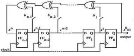
The Linear Feedback Shift Register (LFSR) is a shift register which sequences through (2n-1) states, where n is the total number of shift registers used in designing the LFSR [7]. This is achieved by an array of D flip-flops where, XOR or XNOR gates are used for performing linear functions, as given in Fig.1[4], [6].They are described by the polynomial,
(1)
[image:1.595.324.548.583.677.2]Where the coefficients denoted as represents the polynomial characteristic. LFSR exhibits high-speed bit generation and used in pseudo Noise sequences, digital counters etc. High power utilization is the disadvantage of these generators [4], [5]. LFSRs are frequently used as pseudorandom pattern generators to generate a random number of 1s and 0s. There are two types of LFSR’s-external feedback LFSR’s and internal feedback LFSR’s. The maximum-length of an LFSR sequence is 2n-1.
Fig. -1: Traditional n-bit LFSR
3. POWER GATING TECHNIQUES
3.1 Fine Grain Power Gating (FGPG)
© 2018, IRJET | Impact Factor value: 6.171 | ISO 9001:2008 Certified Journal | Page 3125 transistor is added to every cell that is to be turned off
[image:2.595.308.560.79.199.2]imposes a large area penalty and individually gating the power of every cluster of cells creates timing issues introduced by inter-cluster voltage variation, these are very difficult to resolve.
Fig. -2: Fine Grain Power Gating
3.2 Coarse Grain Power Gating (CGPG)
The CGPG [8] Process implements the grid style sleep transistors which drives cells locally through shared virtual ground and virtual 𝑉𝐷𝐷 networks. This technique introduces
less sensitive to PVT variation & imposes a smaller area overhead than the implementations based on cell- or cluster. In Fig.3 one sleep transistor is added to a cluster of cells.
Fig. -3: Coarse Grain Power Gating
4. IMPLEMENTATION AND RESULTS
D flip-flop and Linear Feedback Shift Register (LFSR) circuits are designed using Cadence Virtuoso tool with 90nm CMOS technology. The transient analysis is done by launching ADEL for verification of schematic results. The power report is obtained for D flip-flop, 16-bit and 32-bit Linear Feedback Shift Register (LFSR) with and without using power gating technique.
4.1 D Flip-Flop
Fig.4 shows the schematic of 2-input NAND gate and 3-input NAND gate respectively. These circuits are used to design the D flip-flop without using power gating.
[image:2.595.107.223.153.282.2]
Fig. -4: Schematic of 2-input and 3-inputt NAND gate
[image:2.595.310.561.275.423.2]Fig.5 shows the schematic of D flip-flop without using power gating. Fig.6 shows the transient response of D flip-flop which is obtained by launching ADEL.
[image:2.595.104.224.420.545.2]Fig. -5: Schematic of D flip-flop
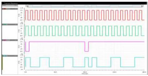
Fig. -6: Transient response of D flip-flop
[image:2.595.308.561.445.609.2]© 2018, IRJET | Impact Factor value: 6.171 | ISO 9001:2008 Certified Journal | Page 3126
Fig. -7: 2-input and 3-input NAND gate used in D flip-flop with FGPG
[image:3.595.39.285.82.207.2]Fig.8 shows the schematic of D flip-flop using Fine Grain Power Gating (FGPG), where one NMOS sleep transistor is inserted between the virtual and actual ground rail of each NAND gate and one PMOS sleep transistor is inserted between the virtual and actual 𝑉𝐷𝐷. Fig.9 shows the transient response of D flip-flop which is obtained by launching ADEL.
Fig. -8: Schematic of a D flip-flop with Fine Grain Power Gating
Fig. -9: Transient response of D flip-flop with Fine Grain Power Gating
Fig.10 shows the schematic of 2-input NAND gate and 3-input NAND gate, where only one NMOS and PMOS sleep transistor needs to be inserted between all the NAND circuits used to design the D flip-flop. These circuits are used to design the D flip-flop with Coarse Grain Power Gating (CGPG).
[image:3.595.308.561.341.460.2]
Fig. -10: 2-input and 3-input NAND gates used in D flip-flop with CGPG
[image:3.595.37.290.344.464.2]Fig.11 shows the schematic of D flip-flop using Coarse Grain Power Gating (CGPG), where one NMOS sleep transistor is inserted between the virtual and actual ground rail of all the NAND gates and one PMOS sleep transistor is inserted between the actual and virtual 𝑉𝐷𝐷. Fig.12 shows the transient response of D flip-flop which is obtained by launching ADEL.
Fig. -11: Schematic of D flip-flop with Coarse Grain Power Gating
Fig. -12: Transient response of D flip-flop with Coarse Grain Power Gating
From Fig.6, Fig.9 and Fig.12 it can be observed that the D flip-flop captures the value of the D-input at a definite portion of the clock cycle (such as the rising edge of the clock). That captured value becomes the Q output. At other times, the output Q does not change.
[image:3.595.306.560.502.633.2] [image:3.595.36.290.507.645.2]© 2018, IRJET | Impact Factor value: 6.171 | ISO 9001:2008 Certified Journal | Page 3127 subsequent changes on the D input will be ignored until the
next clock event.
4.2 16-bit Linear Feedback Shift Register
The 16-bit LFSR is designed for the
polynomial . Fig.13 shows the
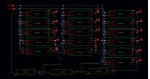
[image:4.595.307.562.74.221.2]schematic for 16-bit LFSR, where the 16-bit LFSR is designed using D flip-flop without using power gating as shown in Fig.5. Fig.14 shows the transient response of 16-bit LFSR.
[image:4.595.34.289.211.343.2]Fig. -13: Schematic of 16-bit LFSR
[image:4.595.308.562.332.474.2]Fig. -14: Transient response of 16-bit LFSR
Fig.15 shows the schematic for 16-bit LFSR with Fine Grain Power Gating (FGPG) technique, where the16-bit LFSR is designed using power gated D flip-flop as shown in Fig.8 and XOR gates. Fig.16 shows the transient response of 16-bit LFSR using FGPG.
Fig. -15: Schematic of 16-bit LFSR with Fine Grain Power Gating
Fig. -16: Transient response of 16-bit LFSR with Fine Grain Power Gating
Fig.17 shows the schematic for 16-bit LFSR with Coarse Grain Power Gating (CGPG) technique, where the LFSR is designed using power gated D flip-flops as shown in Fig.11 and XOR gates. Fig.18 shows the transient response of 16-bit LFSR using CGPG.
Fig. -17: Schematic of 16-bit LFSR with Coarse Grain Power Gating
Fig. -18: Transient response of 16-bit LFSR with Coarse Grain Power Gating
[image:4.595.309.560.518.657.2] [image:4.595.36.290.601.734.2]© 2018, IRJET | Impact Factor value: 6.171 | ISO 9001:2008 Certified Journal | Page 3128 Fig.18 that the sequence repeats after every 65,535 clock
cycles.
5. POWER ANALYSISP
[image:5.595.40.295.192.295.2]The Leakage power dissipation is calculated using Cadence tool Calculator.
Table -1: Power analysis of D Flip-Flop
D flip-flop Maximum Leakage Power Dissipation
D flip-flop without power gating 35.60 uW
D flip-flop with Fine Grain Power
Gating 27.09 uW
D flip-flop with Coarse Grain
Power Gating 15.92 uW
[image:5.595.41.294.437.538.2]Table 1 shows the leakage power of a normal D flip-flop and also power gated D flip-flop’s with Fine Grain Power Gating (FGPG) and Coarse Grain Power Gating (CGPG) techniques. There is 23.90% leakage power reduction in D flip-flop implemented using Fine Grain Power Gating (FGPG) technique and 55.20% leakage power reduction in D flip-flop implemented using Coarse Grain Power Gating (CGPG) technique compared to the normal D flip-flop.
Table -2: Power analysis of 16-bit LFSR
16-bit LFSR Maximum Leakage Power Dissipation
16-bit LFSR without power gating 688.2 uW 16-bit LFSR with Fine Grain Power
Gating 425.6 uW
16-bit LFSR with Coarse Grain
Power Gating 177.5 uW
Table 2 shows the leakage power of a normal 16-bit LFSR and also power gated 16-bit LFSR implemented using D flip-flop’s with Fine Grain Power Gating (FGPG) and Coarse Grain Power Gating (CGPG) techniques. There is 38.15% leakage power reduction in 16-bit LFSR implemented using Fine Grain Power Gating (FGPG) technique and 74.2% leakage power reduction in 16-bit LFSR implemented using Coarse Grain Power Gating (CGPG) technique compared to the normal 16-bit LFSR.
6. CONCLUSION
The 16-bit Linear Feedback Shift Register (LFSR) has been
designed for the polynomial .The
D-flip flop, XOR gate and LFSR were designed using Cadence Virtuoso tool. The leakage power of normal D flip-flop and 16-bit LFSR has been compared with the power gated D flip-flop and 16- bit LFSR, it is observed that there is leakage
power reduction in the power gated circuits when compared to the normal circuits.
Linear Feedback Shift Register with higher order bits can be used to generate pseudorandom test vectors. High fault coverage can be obtained by using more test vectors. Hardware used for LFSR is less and hence it is a preferable for BIST pattern generation.
REFERENCES
[1] Saraswathi T., Ragini. K. and Ganapathy Reddy Ch,“A Review on Power optimization of Linear Feedback Shift Register (LFSR) for Low Power Built In Self Test (BIST)”, Electronics Computer Technology (ICECT), 3rd International Conference, pp. 172-176, 2011.
[2] Balwinder Singh, Arun Khosla and Sukhleen Bindra, “Power Optimization of Linear Feedback Shift Register (LFSR) for Low Power BIST”, Advance Computing Conference, IEEE International, pp. 311-314, 2009.
[3] Chi-Yi Yeh, Hung-Ming Chen, Li-Da Huang, Wei-Ting Wei, Chao-Hung Lu and Chien-Nan Liu, “Using Power Gating Techniques in Area-Array SoC Floorplan Design”, SOC Conference, IEEE International, pp. 233-236, 2007.
[4] Madhushree K. and Niju Rajan, “Dynamic Power Optimization of LFSR Using Clock Gating”, International Conference on Innovations in Information, Embedded and Communication Systems (ICIIECS), vol. 5, pp. 429-432, 2017.
[5] Madhushree K. and Niju Rajan, “Dynamic Power Optimization Using Look-Ahead Clock Gating Technique”, IEEE International Conference On Recent Trends In Electronics Information Communication Technology, pp. 258-262, 2017.
[6] Amit Kumar Panda, Praveena Rajput and Bhawna Shukla, “ FPGA Implementation of 8, 16 and 32 bit LFSR with Maximum Length Feedback Polynomial Using vhdl”, International Conference System and Network Technology, 2012.
[7] Kawal .K, Saluja, “Linaer Feedback Shift Register Theory and Application”, Department of Electronics and Communication Engineering, University of Wisconsin, Madison, Oct 1988.