The empirical dependence of radiation-induced charge neutralization
on negative bias in dosimeters based on the metal-oxide-semiconductor
field-effect transistor
Chris Benson,a兲Abdulrahman Albadri,b兲and Malcolm J. Joycec兲
Engineering Department, Lancaster University, Bailrigg, Lancaster, Lancashire LA1 4YR, United Kingdom
Robert A. Price
Department of Radiography, School of Allied Health Sciences, City University, Northampton Square, London EC1V 0HB, United Kingdom
共Received 6 January 2006; accepted 25 May 2006; published online 22 August 2006兲
The dependence of radiation-induced charge neutralization 共RICN兲 has been studied in metal-oxide-semiconductor field-effect transistor共MOSFET兲 dosimeters. These devices were first exposed to x rays under positive bias and then to further dose increments at a selection of reverse bias levels. A nonlinear empirical trend has been established that is consistent with that identified in the data obtained in this work. Estimates for the reverse bias level corresponding to the maximum rate of RICN have been extracted from the data. These optimum bias levels appear to be independent of the level of initial absorbed dose under positive bias. The established models for threshold voltage change have been considered and indicate a related nonlinear trend for neutralization cross sectionNas a function of oxide field. These data are discussed in the context of dose measurement with MOSFETs and within the framework of statistical mechanics associated with neutral traps and their field dependence. ©2006 American Institute of Physics.
关DOI:10.1063/1.2259814兴
INTRODUCTION
The variation in threshold voltage of metal-oxide-semiconductor 共MOS兲 devices under switched-bias condi-tions is primarily due to the buildup and neutralization of oxide-trapped charge. For the case where the latter has been stimulated by incident radiation, the phenomenon is often termed radiation-induced charge neutralization 共RICN兲. In the context of qualifying commercial integrated circuits共ICs兲 for industrial applications, especially in aerospace, the varia-tion in threshold voltage is often referred to as a parasitic field-oxide transistor shift. Further exposure of a device bi-ased “off,” or indeed with a negative gate potential, acts to reduce the threshold voltage shift. This decreases the leakage current significantly and thereby elevates the failure dose of a dynamically biased part. Therefore, a thorough understand-ing of the dynamics of RICN is important where MOS de-vices are subject to a combination of switched bias and ra-diation exposure.
MOS structures are also being used increasingly for ra-diation dose measurement. This is principally as metal-oxide-semiconductor field-effect transistor 共MOSFET兲 do-simeters for applications in space and for quality assurance in medical radiotherapy. RICN poses a risk in these scenarios because inadvertent reverse biasing of these devices will re-verse and undermine the cumulative dose response of the device. Recovering the dose response analytically, to offset
the effect of this phenomenon, is at best difficult and will often completely undermine the validity of the response.
In contrast to the MOS devices that have been the focus of studies into RICN to date, the MOSFET dosimeter is manufactured with a thick gate oxide, in order to increase its sensitivity to ionizing radiation. Dosimeters based on the
p-MOS field-effect transistor1 are often referred to as MOSFET dosimeters, radiation sensitive field-effect transis-tor 共RADFETs兲,2 or space-charge dosimeters. They have been employed in the measurement of radiation dose in a variety of applications, including those environments associ-ated with particle accelerators and space-bourne satellites. Perhaps the greatest potential for these devices is in the medical sector associated with dose measurement in diagnos-tic or therapeudiagnos-tic radiobiology.
There are several commercial variants and systems cur-rently available3for characterization and quality assurance in external beam radiotherapy.4 The main advantages of the MOSFET dosimeter are that it is small, low power, compara-tively low cost, physically robust, and solid state. The MOSFET dosimeter provides an integrated response and does not require a power supply during irradiation, although improved sensitivity and reduced uncertainty can be afforded under a degree of positive gate bias.
The design of the MOSFET dosimeter has been opti-mized to yield a response that is independent of dose rate5 for low dose-rate applications in space. More recently, the MOSFET dosimeter has found numerous applications in nuclear medicine,6–9for example, in mammography,10 diag-nostic radiology,11 radiotherapy beam profiling,12 and intensity-modulated radiotherapy.13The angular response has been the focus of several recent studies.14,15 Recently, we
a兲Present address: Appleyard Lees, Halifax Office, 15 Clare Road, Halifax
HX1 2HY, UK.
b兲Present address: Riyadh College of Technology, Electronics Department,
P.O. Box 42826, Riyadh 11551, Saudi Arabia.
c兲Electronic mail: [email protected]
共 兲
have explored MOSFET applications in neutron dosimetry,16 the statistical uncertainty in their response to x rays,17 and the development of a linear MOSFET array for intracavatary
in vivodosimetry.18
The process by which the MOSFET responds to radia-tion is well understood. Incident ionizing radiaradia-tion, typically photons, results in the liberation of electron-hole pairs. An electric field is established across the oxide, Eox, either
re-sulting merely from the contact potential of the disparate carrier densities of the neighboring regions or enhanced by applied positive bias, and this causes the carriers to separate and drift. The electrons are swept out of the active region, while the holes are drawn to the interface with the silicon dioxide, where they become trapped. Here the holes act to reduce the depletion region of the device; a phenomenon which can be identified and studied in several ways using electrical characterization tools or impedance measurement. The change in threshold voltageVtcan be decomposed into that due to positive oxide-trapped charge ⌬Vot and negatively-charged interface states ⌬Vit. While well under-stood, the buildup of oxide-trapped charge is a complex, nonlinear process that is dependent on the local field in the oxide, which is itself modulated by the trapped hole popula-tion.
The accepted physical model for RICN was devised by Fleetwood.19 Under positive bias, the process, as described above, results in holes trapped at the Si/ SiO2 interface.
When the bias is switched off,Eoxis induced by the trapped
positive charge and is in the opposite direction; indeed this can be exacerbated by providing negative bias to the gate during subsequent irradiation. With the field reversed, some of the trapped holes at the Si/ SiO2interface are swept to the
gate. However, many remain trapped. Electron-hole pairs lib-erated by the incident radiation are separated, but their direc-tion of travel is reversed in comparison with the correspond-ing phenomenon under positive bias. The electrons migrate to the interface where they can be trapped nearby or recom-bine with the trapped holes. The effect of the radiation on the device’s electrical parameters established under positive bias is thus neutralized.
The objective of the research reported in this paper was to explore and characterize the dependence of RICN with applied reverse bias. This measurement has been performed on devices exposed to two primary dose levels under forward bias. The optimum bias level for RICN has been estimated for each primary dose in both cases. The dependence of RICN with reverse bias has been compared with two empiri-cal mathematiempiri-cal models and the most consistent is deter-mined. The field dependence of RICN beyond the optimum bias indicates a dependence that is reduced in comparison with the known dependence of the recombination cross sec-tionrwith electric field in the oxide. This observation may be due to a combination of compensation and recombination. The field dependence of cross section for RICN N repre-sents the dependence of both phenomena.
EXPERIMENTAL DETAILS
The MOSFET devices used in this work were all sup-plied by the Tyndall Institute, Cork, Ireland. A photograph of
an example MOSFET die is given in Fig. 1. The MOSFET device die is 1 mm2 and comprises of two 300/ 50m 共width/length兲devices and two 690/ 15m devices. The ox-ide thickness of all devices used in this study was 400 nm. This gives each device a natural threshold voltage of be-tween 7 and 8 V; however, the devices used in this study have undergone an implant of boron to reduce the threshold voltage to around 0.5– 2 V. This provides a greater dynamic range for the radiation-induced threshold voltage response.20 A measurement of the threshold voltage of a MOSFET device was made with a reader circuit, as shown in Fig. 2. This arrangement measures the gate-source voltage required to conduct a fixed channel current. In this research a channel current of 10A has been used for this purpose. The setup used in this study to measure the threshold voltage comprises an IBM personal computer共PC兲 housing a Hewlett Packard general purpose interface bus共GPIB兲controller card, which is connected to a Keithley Instruments 2400 sourcemeter. The PC provides control over the sourcemeter through the GPIB; the sourcemeter provides electrical current sourcing and voltage measurement. The sourcemeter is configured in software to provide the 10A channel current through a MOSFET device connected in a two-terminal reader circuit configuration, while simultaneously allowing the
[image:2.612.317.557.49.241.2]measure-FIG. 1. Photograph of a MOSFET dosimeter die.
[image:2.612.373.495.578.742.2]ment of the voltage across its terminals. When the sourcem-eter is connected over GPIB, this system provides an accu-racy of ±1V共one standard deviation from the mean兲. The software used to control the sourcemeter over the GPIB was written in C using MICROSOFT VISUAL C⫹⫹. The threshold voltage was measured 10 s after the initial turn on of supply current to the MOSFET device. This provides a more stable measurement of the threshold voltage since the short-term drift due to border traps21 is reduced.22
The MOSFET dosimeters have been irradiated within a polymethylmethacrylate共PMMA兲phantom to ensure charge equilibrium in the vicinity of the MOSFET and uniform ra-diation dose. The dimensions of the phantom were 300 ⫻300⫻200 mm. The PMMA phantom was placed upon a small 共approximately 10 cm兲 stack of fiberboard in order to allow sufficient depth of material below the MOSFET to ensure the full backscattering of electrons. The MOSFET device, including its 14-pin package, is mounted on a printed circuit board共PCB兲 at a depth of 70 mm below the surface of the PMMA phantom. A narrow channel is provided to allow cabling to connect the device to the measurement and irradiation equipment described above. In order to verify the dose delivered to the MOSFET device, a Farmer dosimeter with a chamber of volume of 0.6 cm3 共type NE 2571兲 was
located at the same depth as the MOSFET device within the phantom. This chamber and related electrometer were cali-brated according to national protocols and factors traced back to national dosimetry standards at the National Physical Laboratory, Teddington, Middlesex, UK. The Doseleader 共type 2610兲calibrated electrometer records the output of this chamber in order to ensure the consistency of the doses delivered.
In order to study RICN, a total of 12p-MOSFET devices were irradiated in two groups of six. All 12 devices were irradiated under a forward bias of +5 V with all other device terminals grounded, which we shall henceforth term “pri-mary” dose. One group of six were irradiated to a primary dose of 48 Gy and the other group to a primary dose of 80 Gy. The threshold voltage of all MOSFETs was measured after this exposure. Each device was then irradiated in dose steps of 4 Gy, with increasing steps in reverse bias. The threshold voltage was measured after each exposure as be-fore. The devices were irradiated to photons produced from an Elekta linear accelerator 共LINAC兲 operated at 6 MV at the Clatterbridge Centre for Oncology National Health Ser-vice共NHS兲Trust, Clatterbridge, UK.
RESULTS
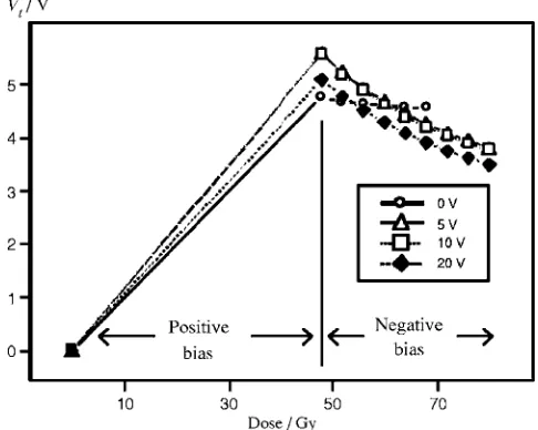
Figure 3 is a plot of the change in threshold voltageVtin volts 共V兲 versus dose in Gray 共Gy兲 for a complete experi-mental cycle of this work. The change in threshold voltage is relative to zero dose, and implicitly we are considering a negative change, since radiation under positive bias leads to a reduction in threshold voltage in the p-MOS transistors used in this research. In Fig. 3 the behavior of the threshold voltage for the primary dose of 48 Gy is shown; similar trends were observed for the primary dose of 80 Gy and are not included in this work in the interests of brevity.
Under positive bias the threshold voltage changes sig-nificantly, following the well-known linear approximation that is valid for small dose levels. This dependence, borne out of an approximation to an exponential trend, is well documented elsewhere for the devices used in this work. For this reason, the data in between the extremes shown here have not been included. Beyond 48 Gy, where the bias has been reversed, the threshold voltage is observed to fall gradually. Similar trends are observed for all levels of nega-tive bias used.
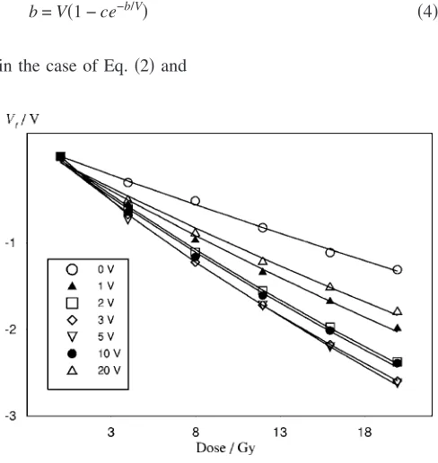
Figures 4 and 5 show the data for threshold voltage change as a function of dose under negative bias for the primary doses of 48 and 80 Gy, respectively. Nonlinear fits have been applied to each data set of the form
Vt共D兲=␣e−D, 共1兲
where ␣ and  are constants and D is dose. Note that the data in Figs. 4 and 5 have been normalized to zeroVtat the point where the bias has been reversed. This removes any variation between the data sets for different devices and cor-responds to a uniform value of ␣ throughout the data. This has been done to extract the rate of Vt recovery, which is described by  in Eq.共1兲. The data for, as a function of negative bias, are given in Table I.
In Fig. 6, the recovery parameter  共Gy−1兲 has been
plotted against negative bias 共V兲, for the case of the two primary doses: 48 and 80 Gy. The uncertainties in  are smaller than the size of the symbols depicting the data. Two empirical fits have been applied to these data. These are
共V兲= a
V
1
eb/V−c. 共2兲
[image:3.612.314.557.51.245.2]The fit provided by this expression关Eq. 共2兲兴has been opti-mized by raising the denominator in the exponent to a vari-able power b. This does not, however, reflect any further physical interpretation,
共V兲= a
V
1
e1/Vb−c, 共3兲
wherea,b, andcare constants for each case. Data for each of the fits listed above are given in Table II.
The degree of negative bias at which optimum RICN occurs corresponds to the bias at whichis maximized. This has been determined via an iterative solution of the deriva-tive of the model used to fit the dependence ofwith nega-tive bias. This procedure has been carried out for Eqs. 共2兲 and共3兲, thus obtaining solutions forVsuch that
b=V共1 −ce−b/V兲 共4兲
in the case of Eq. 共2兲and
b=Vb共1 −ce−1/Vb兲 共5兲
for Eq. 共3兲. These results are given in Table III for each of the primary doses considered in this research, together with the optimum value of in each case.
DISCUSSION
Primary dose dependence and an optimum RICN level
The optimum bias level is observed within uncertainties in the data of 2% and consistently by both expressions 共2兲 and共3兲. The data arising from the two primary doses inves-tigated in this work indicate that the level of primary dose does not appear to influence the bias at which optimum RICN occurs. However, this is clearly only based on two measurements so this interpretation must be treated with caution.
[image:4.612.51.294.49.240.2]The levels of negative bias corresponding to optimum RICN, measured in this work, are consistent with the range in negative bias for optimum RICN rate reported in previous studies.19 However, an approximately constant dependence with reverse bias, as has been suggested, is not observed. The previous studies were of devices with much thinner ox-ides, putting the corresponding oxide field regimes in differ-ent classes and thus increasing the influence of interface TABLE I. RICN recovery parameter 共kGy−1兲as a function of negative
bias共V兲for primary doses of 48 and 80 Gy.
Negative bias共V兲
共kGy−1兲
48 Gy 80 Gy
0 2.10± 0.02 8.40± 0.08 1 9.60± 0.09 12.6± 0.1 2 13.6± 0.1 16.2± 0.2 3 14.2± 0.1 17.6± 0.2
4 ¯ 18.2± 0.2
[image:4.612.311.560.71.243.2]5 13.2± 0.1 17.7± 0.2 10 10.20± 0.09 16.0± 0.1 20 6.00± 0.05 11.4± 0.1
FIG. 4. Relative threshold voltage共Vt兲 change vs dose共Gy兲while under negative bias共data normalized to zero for first datum in all cases兲together with nonlinear fits. Initial dose under positive bias of 48 Gy.
FIG. 5. Relative threshold voltage共Vt兲 change vs dose共Gy兲while under
negative bias共data normalized to zero for first datum in all cases兲together with nonlinear fits. Initial dose under positive bias of 80 Gy.
FIG. 6. Recovery parameter  共Gy−1兲 against negative gate bias 共V兲for
[image:4.612.51.295.465.723.2] [image:4.612.318.557.563.728.2]states significantly. Furthermore, much larger doses were used in comparison with this research. By contrast, the data in this work exhibit a nonlinear dependence on either side of the optimum bias level.
The dependence of recovery with reverse bias
The two fits to the dependence of the recovery parameter
 with reverse bias, shown in Fig. 6, are both acceptable statistical analyses of the RICN data. Expression 共3兲 gives the best representation of the data for both primary doses. If a deeper physical interpretation of RICN data is not required then this is the best model to use. The usual caveat associated with radiation effects in MOS transistors should be borne in mind, i.e., that devices from contrasting fabrication sources will exhibit statistical variation around and possibly beyond the fit parameters given here. However, it is reasonable to expect the trends across MOSFET dosimeters from different manufacturers to be similar. The dependence of RICN with reverse bias observed in this research agrees qualitatively with the hypothesis19that, at high levels of negative bias, the electric field in the oxide transports the electrons past the trapped holes and thus RICN is limited in comparison with that at lower levels of reverse bias. RICN is observed to increase until the optimum because the processes of compen-sation and recombination are encouraged as electrons are transported less rapidly, due to the falling electric field. Be-low the optimum, however, electron transport appears to be incomplete as we approach the positive bias regime; thus RICN falls with further reductions in reverse bias below the optimum, until it eventually ceases completely at the extreme where transport is no longer reversed.
The correspondence ofwith RICN cross section
The statistics of electron trapping are often considered by equating the rate of electron trapping with that of detrap-ping via photon and phonon absorptions. In the case of low electric fields, i.e.,⬍1.5⫻106V cm−1, the cross sections for these detrapping mechanisms are small. Raising the electric
field reduces the energy depth of the trap center which raises the significance of impact ionization and field ionization in detrapping. These influences are often folded into the field dependence of the trapping cross section.23 In addition to Coulombic traps, which acquire charge carriers via tradi-tional charge-based attraction, neutral traps can arise from strained molecular bonds in the oxide’s atomic lattice. The cross section of these is likely to have a less-pronounced field dependence because of the much shorter effective range of the potential of the neutral trap.24
In this work the maximum oxide electric fieldEox was
5⫻105 V cm−1. Electron capture by Coulomb-attractive
oxide-charge centers, leading to recombination, is known to be a strong function of the average oxide field.25 For Eox
⬍106V cm−1共this case兲the cross section for recombination
ris known to vary approximately asEox−3/2. The data beyond
the point of optimum RICN共for negative bias levels greater than 3 V兲 do not exhibit even an approximate correspon-dence with this depencorrespon-dence. Instead a much reduced depen-dence of approximatelyEox−1/3is observed. Clearly, a signifi-cant shortcoming of our work is that in this region there are very few data. However, the inconsistency of the field depen-dence may support the possibility of a combined role of re-combination and compensation in RICN, as opposed to that of recombination alone. Alternatively, the neutralization phe-nomenon may be due to the localized trapping of electrons in neutral traps, thus exhibiting the less pronounced field de-pendence described above.
Returning to Eq.共2兲 and considering RICN in terms of recombination cross sectionr, we can draw correspondence with the known dependence of this25 with threshold voltage change Vt:
Vt=
qNTT¯x Kox⑀0
关1 −e−rNinj兴. 共6兲
HereNTTis the number of trap centers per unit area,¯xis the centroid of the trap distribution, Kox is the static dielectric
constant of SiO2,Ninj is the number of electrons introduced
per unit area, q is the charge of an electron, and ⑀0 is the
permittivity of a vacuum. If Vtin Eq. 共1兲is considered as a saturating quantity, i.e.,Vt=␣共1 −e−D兲, for comparison with Eq. 共6兲 where  is identical to that defined in Eq. 共1兲, the following proportionality can be inferred:
NNinj⬀D. 共7兲
[image:5.612.124.487.77.149.2]Here correspondence is drawn with radiation dose being the source of carriers as opposed to hot electron injection tech-niques. The latter have often been used to introduce carriers in experiments to measure the field dependence of trapping TABLE II. Fit parameters for various models to describe the variation of RICN recovery parameterwith
negative bias.
Model
Coefficients of fits共primary dose of 48 Gy兲 Coefficients of fits共primary dose of 80 Gy兲
a共V Gy−1兲 b共V兲 c
2 a共V兲 b共V兲 c
2
Equation共3兲 0.018 1.231 0.883 1.746 0.022 1.081 0.947 1.415 Equation共2兲 0.040 1.607 0.767 2.719 0.030 1.216 0.936 1.740
TABLE III. Negative bias values for optimum levels of RICN recovery parameter共kGy−1兲, for primary doses of 48 and 80 Gy, arising from Eqs. 共2兲and共3兲.
Model Primary absorbed dose
Negative bias共V兲
Optimum共kGy−1兲
48 Gy 80 Gy
[image:5.612.49.297.680.756.2]cross sections. Therefore N has been introduced in Eq.共7兲 as the cross section for RICN, to reflect the combined role of compensation and recombination of electrons and holes in the oxide. Since it has been shown that  is a function of oxide field, it follows thatNwill also exhibit a related de-pendence, i.e.,共Eox兲and共Eox兲,
N共Eox兲⬀
共Eox兲D Ninj
. 共8兲
Thus the experimental measurement of the dependence of with reverse bias provides a qualitative means for character-izing the dependence of cross section for RICN with electric field across the oxide.
The implications for dose measurement
RICN is unlikely to be of use in mainstream dosimetry with MOS devices. However, in extreme circumstances where switch-bias conditions arise, either inadvertently or otherwise, the dependence of the neutralization of trapped charge with reverse bias will be crucial if adjustments are sought to account for the effect of the exposure under reverse bias. This may, for example, be of particular value where MOS devices are inaccessible and cannot be replaced easily, such as in space. Furthermore, the possible independence of optimum RICN bias with primary dose suggests that allow-ance for switch-bias effects could be made with reference to this optimum recovery level and the dependence of with bias reported in this research.
CONCLUSIONS
The dependence of RICN with reverse bias has been measured for doses consistent with therapeutic uses of these devices, up to 20 Gy. Correspondence between the depen-dence of RICN with reverse bias and the dependepen-dence of neu-tralization cross section with oxide electric field has been made. In summary, this work can be concluded as follows.
共1兲 For high levels of negative bias, the degree of RICN falls off to very low levels, consistent with the works of Fleetwood19 and of Freitaget al.26
共2兲 In the high-level, reverse bias extreme, the degree of RICN is very low but it is observed to be greater than that for very low levels of reverse bias, i.e., for bias levels greater than −1 V.
共3兲 The dependence of RICN between −1 and −6 V is ob-served to be nonlinear and a maximum is obob-served in this region.
共4兲 The reverse bias level at the optimum RICN is consis-tent with the region identified previously,19 correspond-ing to the region in which the gradient of the threshold voltage change versus reverse bias is maximized. 共5兲 The observation that an optimum bias exists for RICN
suggests that it is at this point that the field due to the oxide trap charge becomes greater than the applied gate bias. If this is the case, then charge transport at this
optimum level must be small, due to the fields essen-tially canceling each other. Hence this provides further evidence for the location of the H+ions responsible for
making the interface traps being very near the Si/ SiO2
interface.
共6兲 A proportional relationship exists between the cross-section dependence of RICN with oxide field and that of the experimental recovery parameter  observed as a result of RICN measurements.
共7兲 The dependence of RICN versus reverse bias follows an empirical dependence consistent with Eq. 共2兲. More re-search is necessary to determine how primary dose in-fluences the reverse bias level associated with optimal RICN.
ACKNOWLEDGMENTS
We gratefully acknowledge the support and assistance of the Engineering and Physical Sciences Research Council 共EPSRC兲, the Clatterbridge Centre for Oncology, and the General Organization for Technical Education and Voca-tional Training, Riyadh, Saudi Arabia.
1L. S. August, IEEE Trans. Nucl. Sci. 29, 2000共1982兲. 2A. Holmes-Siedle, Nucl. Instrum. Methods 121, 169共1974兲. 3A. Jones and D. Hintenlang, Health Phys. 82, S130共2002兲. 4A. B. Rosenfeld, Radiat. Prot. Dosim. 101, 393共2002兲.
5J. R. Schwank, S. B. Roeske, and D. E. Beutler, IEEE Trans. Nucl. Sci.
43, 2671共1996兲.
6M. W. Bower and D. E. Hintenlang, Health Phys. 75, 197共1998兲. 7M. J. Butson, A. Rosenfeld, J. N. Mathur, M. Carolan, T. P. Wong, and
P. E. Metcalfe, Med. Phys. 23, 655共1996兲.
8K. Y. Quach, J. Morales, M. J. Butson, A. B. Rosenfeld, and P. E.
Metcalfe, Med. Phys. 27, 1676共2000兲.
9R. Ramani, S. Russell, and P. O’Brien, Int. J. Radiat. Oncol., Biol., Phys.
37, 959共1997兲.
10S. L. Dong, T. C. Chu, J. S. Lee, G. Y. Lan, T. H. Wu, Y. H. Yeh, and
J. J. Hwang, Appl. Radiat. Isot. 57, 791共2002兲.
11S. L. Dong, T. C. Chu, G. Y. Lan, T. H. Wu, Y. C. Lin, and J. S. Lee,
Appl. Radiat. Isot. 57, 883共2002兲.
12T. Kron, A. Rosenfeld, M. Lerch, and S. Bazley, Radiat. Prot. Dosim.101,
445共2002兲.
13C. F. Chuang, L. J. Verhey, and X. Ping, Med. Phys. 29, 1109共2002兲. 14J. N. Roshau and D. E. Hintenlang, Health Phys. 84, 376共2003兲. 15B. D. Pomije, C. H. Huh, M. A. Tressler, D. E. Hintenlang, and W. E.
Bolch, Health Phys. 80, 497共2001兲.
16R. A. Price, C. Benson, M. J. Joyce, D. J. Kestell, and J. Silvie,
Radiat. Prot. Dosim. 110, 283共2004兲.
17C. Benson, R. A. Price, J. Silvie, A. Jaksic, and M. J. Joyce, Phys. Med.
Biol. 49, 3145共2004兲.
18R. A. Price, C. Benson, M. J. Joyce, and K. Rodgers, IEEE Trans. Nucl.
Sci. 51, 1420共2004兲.
19D. M. Fleetwood, J. Appl. Phys. 67, 580共1990兲.
20Y. P. Tsvidis, Operation and modelling of the MOS transistor 共Oxford University Press, New York, 2003兲.
21D. M. Fleetwood, IEEE Trans. Nucl. Sci. 39, 269共1992兲.
22Z. Savic, B. Radjenovic, M. Pejovic, and N. Stojadinovic, IEEE Trans.
Nucl. Sci. 42, 1445共1995兲.
23D. A. Buchanan, M. V. Fischetti, and D. J. DiMaria, Phys. Rev. B 43,
1471共1991兲.
24S. K. Lai, J. Appl. Phys. 54, 2540共1983兲. 25T. H. Ning, J. Appl. Phys. 47, 3203共1976兲.
26R. K. Freitag, C. M. Dozier, and D. B. Brown, IEEE Trans. Nucl. Sci.