Future Generation Ultra Supercomputing 256 × 256 Bits
Multiplier for Signed-Unsigned Number
Ravindra P Rajput *, M. N Shanmukha Swamy **
*
Electronics and Communications Engineering, JSS Research Foundation, Mysore University, Mysore, Karnataka, India. **
Electronics and Communications Engineering, SJCE, Mysore, Karnataka, India.
Abstract- With the future 1 nm Hybrid CMOS technology, we proposed the Future Generation Ultra Supercomputing 256 × 256 Bits Multiplier for Signed-Unsigned Number. The Hybrid CMOS consists of the CMOS and Complimentary Pass Transistor Logic (CPTL). With the 1 nm future technology the various parameters predicted are the critical path delay of 0.1 ns (10 GHz), chip area of 136.23 𝛍m2 and the power dissipation of 1171.4 𝛍W.
Index Terms- MMBE, CPTL, PPG, VCA, PPRT, CLCSA, CMOS Technology.
I. INTRODUCTION
uture generation ultra supercomputers and requires ultra high speed multipliers. The matrix data multiplication by the supercomputers has wide range of applications such as weather forecasting, oil and gas exploration under the sea, molecular modeling, DNA testing etc. Supercomputer uses the concept superscalar; in this technique up to 8 instructions can be fetched and executed in parallel. There can be more than two dedicated multiplier units in the functional unit of a supercomputer. To meet the requirements of future applications the design of ultra supercomputer is essential. The ultra supercomputing speed may be required to forecast about natural calamities such as the earthquake, tsunami etc. Such applications needs to process huge matrix data from the sensors located at the remote place. Since, multiplication is the most time critical, most area and power consuming operation, the specialized design of multipliers for least delay, smallest in area and lowest in power consumptions are essential.
All the high speed parallel multiplication operation in hardware consists of three phases as follows.
1. Partial Product Generator (PPG).
2. Partial Product Reduction Tree (PPRT).
3. 3. Carry Propagate Adder (CPA).
Since, the performance of the multipliers can be enhanced by designing high speed PPG circuits, many recent advanced paper [1]-[3] has been published. Since, the performance of the multipliers can also be enhanced to the most extent by designing high speed PPRT, many high performance papers [4]-[6] has been published. And finally since, the maximum speed of the multipliers depends on the performance of the
Carry Propagate Adder (CPA), various high speed CLA techniques have published in papers [7]-[10].
References [1]-[3] have presented the design of MBE architecture to generate a partial products in parallel. Reference [1] presented the design of PPG with 68 transistors in CMOS logic, and delay, area and power consumption measured has 0.033 ns/bit, 7.83 𝛍m2/bit and 1.81 𝛍W /bit respectively. Reference [2] presented the design of PPG with 56 transistors in CMOS logic, and its delay, area and power consumption measured has 0.029 ns/bit, 0.13 𝛍m2/bit and 1.62
𝛍W /bit respectively. Reference [3] presented the design of PPG with 56 transistors in CMOS logic, and its delay, area and power consumption measured has been 0.045 ns/bit, 0.12
𝛍m2/bit and 1.65 𝛍W /bit respectively.
The second phase of the multiplier PPRT. Whose function is to reduce the n number of partial products to two only. Reference [4] presented the design of a PPRT using Three Dimensional Minimization (TDM) Method. The TDM has implemented with 98 transistors in CMOS logic, and its delay, area and power consumption measured has 0.06 ns, 30.87 𝛍m2 and 26.43 𝛍W respectively. Reference [1] has used the concept of reference [4] as PPRT.
Reference [5] presented the design of 4:2 and 5 :2 compressors. The 4:2 compressor has implemented with 60 transistors in CMOS logic, and its delay, area and power consumption measured has 0.047 ns, 18.9 𝛍m2 and 20.67 𝛍W respectively. The 5:2 compressor takes 7-inputs and produces 4 outputs namely three carry and a sum. The 5:2 compressor has implemented with 90 transistors in CMOS logic, and its delay, area and power consumption measured has 0.06 ns, 28.35 𝛍m2 and 24.3 𝛍W respectively.
Reference [6] presented the design of Wallace tree for the addition of 7-bits of the PPRT, and the number of transistors, delay, area and power consumption has been same as the reference [6].
HERE TO EDIT) <
II. PROPOSED256×256BITSMULTIPLIER
This multiplier is designed predicting the future 1 nm CMOS technology to the requirements of next generation ultra supercomputers. Fig. 1 shows the block diagram of super fast multiplier based on MMBE logic. Its operation is based on the concept of 4 to 1 multiplexer, and this is called as partial product generator (PPG). The MMBE produces all the partial products in parallel. Table I shows the truth table of proposed MMBE scheme. From table I equations (1) – (5) are obtained.
Where the symbol ‘ ‘ represents exclusive OR operation. For the Equations (1) to (4) MMBE logic diagram is as shown in Fig. 2. And using hybrid CMOS logic with 16 transistors is implemented as shown in Fig. 3. According to the input multiplier operand b, the MMBE logic selects 0, a, 2a, −a,
−2a to generate the partial product rows in parallel. In equation (1) when si = 1, MMBE selects −2a or +2a. And
when zi= 1, the MMBE selects – a, + a. The negateoperation
is achieved by one’s complimenting each bit of a and then adding ni = 1 to the least significantbit. The negate operation
is implemented using equation (5).
TABLEI
TRUTH TABLE OF NMBE SCHEME
bi+1 bi bi-1 Operation zi si ni
0 0 0 +0 0 0 0
0 0 1 +a 1 0 0
0 1 0 +a 1 0 0
0 1 1 +2a 0 1 0
1 0 0 -2a 0 1 1
1 0 1 -a 1 0 1
1 1 0 -a 1 0 1
1 1 1 -0 0 0 0
[image:2.612.51.554.197.726.2]Fig. 1. Block diagram of proposed multiplier. n-bit multiplicand bn-1 bn-2 …… b1 b0 n-bit multiplier an-1 an-2 …… a1 a0 p = a×b Partial Product Reduction Tree (PPRT) Carry Propagate Adder (CPA) (n/2)+1 Partial Product Generator (PPG) SU Logic an-1 bn-1 s_u an bn xi+1 = bi+1 ai+1, xi = bi+1 ai (4)
zi = bi+1 bi-1 (3)
pij = xi+1 si + xi zi (1)
ni = bi+1 ( bi-1 bi ) (5)
si =bi bi+1 (2)
Fig. 2. Logic diagram of MMBE bi+1 bi bi-1 0 ai ai+1 pij 4: 1Multiplexer 0 1 2 3
Fig. 3. Circuit diagram of MMBE ai+1
ai
bi-1
bi
bi+1
pij
Fig. 4. Sign converter logic.
s_u
b
n-1
a
n-1
b
n
a
n
Fig. 5. Logic diagram for final bit of final row of PPG.
P
ijs_u
[image:2.612.49.302.198.399.2]Fig. 4 shows the logic diagram of sign converter. A mode signal called signed-unsigned (s_u) is used to indicate whether the multiplication operation is for signed or unsigned number.
When
s_u = 0, indicates unsigned number multiplication. s_u = 1, indicates signed number multiplication
For unsigned number multiplication, the requirement of 0 sign extended bit is as given in equation (6), and for the signed multiplication the sign extended bits required are given by the equations (7) and (8). Equation (9) generates a bit for signed-unsigned multiplication operation.
an = an+1 = bn = bn+1 = 0 (6)
s_u = 1, an-1 =1, bn-1 = 0, an = an+1 =1, bn = bn+1 = 0 (7)
s_u = 1, an-1 =0, , bn-1 = 1, an = an+1 = 0, bn = bn+1 =1 (8)
Where i = n-1, j = n-1.
Our proposed design of 256 bits multiplier is based on the prediction of the future 1 nm process technology. The various parameters required for the future process technology is explained as follows. For 1 nm process technology the delay of NMOS transistor is computed as follows.
Where L is the length of the channel and for 1 nm technology L is 1 nm, 𝛍n is the electron mobility carrier and its typical value at room temperature is 550 cm2 / V sec, and for Vds =
1.8 V supply voltage, Td = 0.01×10⁻¹⁵second = 0.01 fs (femto second).
For 1 nm process technology the delay of PMOS transistor is computed as follows.
Where L is the length of the channel and for 1 nm technology L is 1 nm, 𝛍p is the hole mobility carrier and its typical value at room temperature is 240 cm2 / V sec, and for Vds = 1.8 V
supply voltage, Td = 0.023×10⁻¹⁵second = 0.023 fs (femto
second). But for the CMOS inverter shown in Fig. 6 when PMOS is turned ON, its resistance RON is about 4.5 KΩ, then
the switching speed of inverter reduces to 0.1 ps (pico second). The CMOS inverter delay measured by 45 nm technology has 0.006 ns, when CMOS technology decreases to 1 nm, then delay decreased to 0.006/25 = 0.24 ps. And thus the delay for the MMBE shown in Fig. 3 consists of 4 inverter delay is computed as follows.
Delay of MMBE (TMMBE) = 4 × 0.24 ps = 0.96 ps
For the layout of CMOS inverter shown in Fig, 7, area is computed as follows.
Area = 34λ × 14λ
With λ =
1 nm
Area = 34 × 14λ = 476 nm2
The MMBE circuit of Fig. 3 uses 8 inverters, and the area is computed as follows..
.
MMBE area (AMMBE) = 8 × 476 nm2 = 3808 nm2
For 256 bits multiplier, there are 33280 MMBE’s, thus the total area occupied by the MMBE is computed as follows.
Total MMBE area (ATMMBE) = 3808 × 33280 nm2
= 126.73 µm2
The power dissipated (Pd) by MMBE is computed as follows.
Pd = N F C V 2dd
N = Number of transistor
F= Frequency = 10 GHz Capacitance (C) = 0.0001× 10⁻¹⁵F Power supply (Vdd) = 1.8 V
The power dissipated by the MMBE (PMMBE) is computed as
follows.
PMMBE = 258 × 129 × 10 × 10 ×109 × 0.0001 × 10-15×1.82
= 1078.3 µW L2
𝛍nVds Tdp =
L2
𝛍nVds Tdn =
Pij = s_u an-1 an-2 (9)
34λ
GND
14λ
Vin Vout
[image:3.612.318.569.30.241.2]Fig. 7: Layout of CMOS inverter.
Fig. 6: Circuit diagram of CMOS inverter.
Vin. Vout
HERE TO EDIT) <
III. DESIGN OF VCA
Our proposed Vertical Column Adder (VCA) is based on the concept of references [4], [6] which presented the design of a PPRT with minimum delay. In this method, each column partial product bits of that column and carry bits generated by the previous column has been added to produce a sum bit and the number of carry bits. The carry bits from the previous column have been fed as input to the full adder so that the delay of the VCA has been the minimum. Fig. 8 (a) shows the circuit diagram of full adder, and is implemented in CMOS logic using only 10 transistors. Fig. 8(b) shows the circuit diagram of SCGP logic, this is the final cell of each VCA. Where cpi is called carry propagate term, and cgi is called
carry generate term This is designed to perform operations such as sum, carry generate and carry propagate terms so as to save the extra hardware for carry generate and carry propagate terms and is implemented in CMOS logic using only 10 transistors.
For 256 bits multiplier there are 256 VCA’s, and VCS’s are implemented using full adders. Each full adder is implemented using 5 inverters. Therefore, the delay and area are computed as follows/
PPRT delay (TPPRT ) = 41.48 × 10 -12
PPRT area = 2496 × 5 × 476 nm2
= 5.92 µm2
The power dissipated by the PPRT is computed as follows.
PPPRT = 2496 × 10 × 10 ×109 × 0.0001 × 10-15×1.82
= 80.87 µW
Thus, the delay, area and power dissipated by the 256 bits multiplier is computed as follows.
IV. DESIGNOFCPA
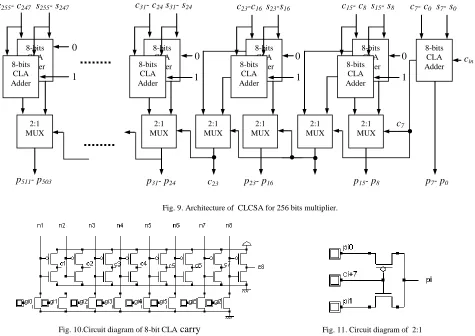
The final adder which combines the effect of Carry Lookahead Adder and Carry Select Adder (CLCSA) is as shown in Fig. 11. The 8-bit CLA adder is designed and is used in cascade through carry select adder technique for high performance. All the 8-bit CLA adders produce carry in parallel and there are two such 8-bit CLA’s in each stage with 0 and 1 as the initial carry input. If the final carry output from the previous stage of 8 bit CLA is 1 then the output selected by the 2:1 multiplexer is the output of the CLA adder with 1-input as the initial carry. Carry expressions for 8-bit CLA adder’s are as follows.
c1 = g0 +p0cin
c2 = g1 + p1 g0 + p1p0cin
c3 = g2 + p2 g1 + p2 p1g0 + p2p1p0cin
c4 = g3 + p3g2 +p3p2g1 + p3p2 p1g0 + p3p2p1 p0cin
c5 = g4 + p4g3 + p4p3g2 + p4p3p2g1+ p4p3 p2p1g0
+ p4p3 p2p1p0cin
c6 = g5+p5g4 + p5p4g3+ p5p4p3g2 + p5p4 p3 p2g1+ p5p4 p3 p2p1g0
+ p5p4p3 p2p1p0cin
c7 = g6 + p6 g5 + p6 p5g4 + p6 p5p4g3 + p6 p5 p4 p3 g2
+ p6 p5 p4 p3 p2g1+ p6 p5 p4 p3 p2 p1+ p6 p5 p4 p3 p2p1p0cin
c8 = g7+p7g6+ p7p6 g5 + p7 p6 p5 g4 + p7 p6 p5 p4 g3
+ p7 p6 p5p4p3g2 + p7p6 p5 p4p3 p2 g1
+ p7 p6 p5p4p3 p2 p1g0 + p7 p6 p5 p4 p3 p2 p1p0cin
Equations c1 through c8 are implemented as shown in Fig. 9.
Inputs g0 through g7 has provided from the SCGP circuit of
Fig. 9 (b). The inputs n1 through n8are the outputs of nand
gates, where n1 is the output of 2-inputs nand gate, n2 is the
output of three inputs nand gate, and n3, n4, n5, n6, n7, n8 are
[image:4.612.105.242.286.554.2]outputs of 4, 5, 6, 7 and 8 inputs nand gates respectively. This has been implemented using only 94 transistors. The critical delay measured is 0.05ns.
Fig. 8. Architecture of full adder. (a). Logic diagram. (b) Circuit diagram. (c) Circuit diagram of SCGP.
(a)
xi+1
xi+2
ci
ci+1 si
(b) cgi cpi xi+1
xi+2
ci
The delay of CLCSA is computed as follows.
TCLCSA = 0.045 ns/25 = 1.8 ps
For 256 bits multiplier 32 CLCSA’s are required, and its delay is computed as follows.
TCLCSA = 0.045 ns/25 = 32 × 1.8 ps = 57.6 ps
The area for CLCSA is computed as follows.
8-bits CLCSA area = 59 × 476 nm2 = 0.028 µm2
For 256 bits multiplier 64 CLCSA’s are required
256 bits CLCSA area = 128 × 0.028 µm2
= 3.58 µm2
The power dissipated by the CLCSA is computed as follows.
PdCLCSA = 64 × 59 × 10 ×109 × 0.0001 × 10-15×1.82
= 12.23µW
V. THEORETICALRESULTS
The critical path delay of 256 × 256 Bits multipliers can be computed by using equation as follows.
Delay T256 = TMMBE + TPPRT + TCLCSA
= 0.92 × 10⁻¹² + 41.48 × 10⁻¹² + 57.60 × 10-12
= 0.1× 10⁻⁹s = 0.1 ns
Area A256 = AMMBE + APPRT + ACLCSA
= 126.73 µm2 + 5.92 µm2 + 3.58 µm2
= 136.23 µm2
Power P256 = PMMBE + PPPRT + PCLCSA
= 1078.3 µW + 80.87 µW + 12.23µW
= 1171.4 µW
Fig. 11. Circuit diagram of 2:1
[image:5.612.66.541.77.413.2]multiplexer.
Fig. 10.Circuit diagram of 8-bit CLA carry generator.
.
s7- s0
2:1 MUX
c7 2:1
MUX
s15- s8 c15- c8 c31- c24s31- s24
p7- p0 c23
8-bits CLA Adder 8-bits
CLA Adder
0
1
p15- p8 p23- p16
p31- p24
c7- c0 c23-c16 s23-s16
cin 8-bits
CLA Adder 8-bits
CLA Adder
0
1
2:1 MUX
8-bits CLA Adder 8-bits CLA Adder
0
1
2:1 MUX 2:1
MUX
8-bits CLA Adder 8-bits
CLA Adder 8-bits
CLA Adder
2:1 MUX
p511- p503 c255- c247 s255- s247
0
1
HERE TO EDIT) <
These theoretical results listed in table I.
VI. CONCLUSION
Our proposed “Future Generation High Performance, Area Efficient And Low Power Multiplier Operating at 10 GHz”. With the future 1 nm Hybrid CMOS technology, the various parameters of the 256 × 256-Bit multiplier are the critical path delay of 0.1 ns, and with this delay it can operate with 10 GHz frequency, with chip area of 136.23 𝛍m2 and the power dissipation of 1171.4 𝛍W. These results shows the better performance of our proposed multiplier.
ACKNOLEDGEMENT
The authors would like to acknowledge the J S S Research foundation, SJCE Campus, Mysore, for all the facility provided for this research work.
REFERENCES
[1] W. –C. Yeh and C. –W. Jen, “High Speed Booth encoded Parallel Multiplier Design,” IEEE transactions on computers, vol. 49, no. 7, pp. 692-701, July 2000.
[2] Shiann-Rong Kuang, Jiun-Ping Wang, and Cang-Yuan Guo, “Modified Booth multipliers with a Regular Partial Product Array,” IEEE Transactions on circuits and systems-II, vol 56, No 5, May 2009. [3] Gensuke Goto, Atsuki Inoue, Ryoichi Ohe, Shoichiro Kashiwakura,
Shin Mitarai, Takayuki Tsuru, and Tetsuo Izawa, “A 4.1 ns Compact 54×54-b Multiplier Utilising Sign-Select Booth Encoders”, IEEE journal of solid-state circuit, VOL. 32, NO. 11, November 1997.
[4] Vogin G. Oklobdzija, David Vileger, Simon S. Liu, “A Method for Speed Optimized Partial Product Reduction and Generation of Fast Parallel Multipliers Using an Algorithmic Approach”,IEEE transaction on computers, Vol. 45, No. 3, pp. 294-306, March 1996.
[5] C.-H. Chang, J. Gu, and M. Zhang, “Ultra low-voltage low-power CMOS 4–2 and 5–2 compressors for fast arithmetic circuits,” IEEE Trans.Circuits Syst. I, Reg. Papers, vol. 51, no. 10, pp. 1985–1997, Oct. 2004.
[6] C. S. Wallace, “A Suggestion for a Fast Multiplier”, IEEE Transaction on Electronic Computers, pp. 14-17, February 1964.
[7] Radu Zlatanovici, Sean Kao, and Borivoje Nikolic´ “A 240 ps 64 b carry-lookaheadadder in 90 nm CMOS,” IEEE journal of solid-state circuit,, VOL. 44, NO. 2, pp.569-583, February 2009.
[8] II: Analog and Digital Signal Processing,, VOL. 43, NO. 10, OCTOBER 1996, pp.689-702.
[9] T. P. Kelliher, R. M. Owens, M. J. Irwin, and T.-T. Hwang, “ELM-A Fast Addition Algorithm Discovered by a Program”, IEEE Trans. Comput,VOL. 41, NO. 9, September 1992, pp.1181-1184.
[10] Amaury Nève, Helmut Schettler, Thomas Ludwig, Denis Flandre,,”Power-Delay Product Minimization in High-Performance 64-bit Carry Select Adders”, IEEE Trans. Very Large Scale Integr. Systems, VOL. 12, NO. 3, pp.235-244, MARCH 2004.
AUTHORS
First Author – Ravindra P Rajput
received the BE degree in Electronics and Communication Engineering from Karnataka University Dharwad in 1996, M.Tech degree in Digital Electronics from Visvesvaraya Technological University, Belgaum in 2000. He is currently pursuing the PhD degree from Mysore University, Mysore. He is presently working as Associate Professor in the Department of Electronics and Communication, University BDT College of Engineering, Davanagere, Karnataka, India. He has published many books and papers in international conferences and Journals. His research interests include VLSI design, computer architecture, embedded systems, digital signal processing, Advanced microprocessors, design of high speed multipliers, Design of high speed adders.
Second Author – Dr. M. N.
Shanmukha Swamy received the BE degree in Electronics and Communication Engineering from Mysore University in 1978, M.Tech degree in Industrial Electronics from the same University in 1987, and obtained his Ph.D. in the field of Composite materials from Indian Institute of Science, Bangalore in 1997. He is presently working as Professor in the Department of Electronics and Communication, Sri Jayachamarajendra College of Engineering, Mysore, Karnataka, India. He is guiding several research scholars and has published many books and papers both in national and international conferences and Journals. His research area includes Wireless Sensor Networks, Biometrics, VLSI and composite materials for application in electronics.
Correspondence Author – Ravindra P Rajput,
[email protected] , 9886083949.
Reference [3] 0.24 9041.6 3007.7 Table – 2 Comparison of multipliers
256×256
Reference [2] 0.23 10464.8 3206.0
Proposed 0.10 136,23 1171.4 Multiplier References Delay Area Power Size (ns) (𝛍m2 ) (𝛍W)