N A N O E X P R E S S
Open Access
Fabrication and characterization of well-aligned
plasmonic nanopillars with ultrasmall separations
Guangyuan Si
*, Xiaoxiao Jiang, Jiangtao Lv, Qiongchan Gu and Fengwen Wang
Abstract
We show the fabrication of well-aligned gold and silver nanopillars with various array parameters via interference lithography followed by ion beam milling and compare the etching rates of these two metallic materials. Silver is suitable for fabricating ultrafine arrays with ultrasmall separations due to high milling rates. The optical properties of the fabricated nanopillars are specifically characterized from both normal incidence and oblique incident angles. Tunable surface plasmon resonances are achieved with varying structural parameters. Strong coupling effects are enabled when the separation between adjacent nanopillars is dramatically reduced, leading to useful applications in sensing and waveguiding.
Keywords:Plasmonic; Nanopillars; Dense arrays
Background
Known as the electromagnetic waves propagating along metal-dielectric interfaces, surface plasmons (SPs) have drawn increasing attention in recent years [1-5]. Many plasmon-enabled applications have been developed due to their unique optical properties and particular ability of manipulating light at the nanometer scale. Additionally, SP-based waveguides are useful for developing devices with ultrahigh sensitivity and figure of merit because the near-field of electromagnetic waves can be significantly enhanced using different plasmonic nanostructures. Vari-ous plasmonic nanostructures, including nanopillars for waveguiding [6-8], and bio-sensing [9-11], or photonic crystals for efficient cavity coupling [12], have been dem-onstrated recently. Moreover, extensive useful applications have been triggered by plasmonics in super-resolution imaging [13-15], cloaking [16-18], energy harvesting [19-21], and color filtering [22-25]. Various applications (plasmonic absorbers, for instance) have been reported by using nanodisks [26-28] or nanopillars [29] to mod-ify the surface profile, allowing for tight confinement of more energy inside the functional layer of a solar cell. Such nanodisks/nanopillars that act as plasmonic ab-sorbers (also known as plasmonic blackbodies) are ex-tremely useful for energy harvesting. Metal nanopillars
or wires excited by electromagnetic waves show resonance characteristics which are highly dependent on geometric parameters. In the optical regime, metals are dispersive materials with finite conductivity. Either surface plasmon polaritons (SPPs) or localized surface plasmon resonances (LSPRs) reveal salient resonance features, and the optical properties of metal nanopillars are mainly determined by their shape, size, and even the dielectric environment. Recently, the fascinating optical properties of small nanopillars/particles [30-34] and other different geom-etries [35-40] have been extensively investigated both experimentally and theoretically, providing a new path-way for manipulating light at the subwavelength scale.
Due to important advances in nanofabrication tech-niques, plasmonic nanostructures and related devices are presently gaining tremendous technological significance in nanophotonics and optics. Nanostructures could provide intriguing possibilities for resolving those challenges and improving device performance. Well-aligned nanopillars with perpendicular orientations to the substrate are be-coming the main building blocks for new optical devices with promising potential applications [41]. Here we ex-plore, experimentally and theoretically, the optical proper-ties of periodic nanopillars perpendicularly aligned on the supporting substrate. Combination of interference lithography (IL) and ion beam milling (IBM) techniques enables scalable fabrication of such nanopillars with excel-lent dimensional control and high uniformity. Detailed * Correspondence:siguang0323@hotmail.com
College of Information Science and Engineering, Northeastern University, 110004 Shenyang, China
experimental results show that silver (Ag) has a much higher etching rate than gold (Au) under the same milling conditions, making Ag a perfect candidate for the con-struction of plasmonic ultrasmall features. In addition, nanopillar arrays with ultrasmall inter-pillar separations are fabricated and optically characterized.
Methods
Quartz substrates were first cleaned with acetone in an ultrasonic bath followed by isopropyl alcohol (IPA) and deionized water washing and finally blow-dried with a nitrogen gun. Subsequently, Au or Ag films with differ-ent thicknesses were deposited on quartz substrates with 4-nm titanium as the adhesion layer by electron beam evaporation (Auto 306, Edwards, Crawley, UK) at a base pressure of about 3 × 10⁻⁷mbar. In order to minimize the
deposition-introduced roughness, low evaporation rates were applied (less than 0.03 nm/s). Afterwards, positive resist (S1805, Dow, Midland, MI, USA) was used to define nanopillar arrays on the metal (Au or Ag) layer supported by a quartz substrate (refractive index = 1.46) with a laser holography system using a 325-nm helium-cadmium laser, serving as the IBM mask after development.
During the IBM process (Microetch 1201, Veeco In-struments, Plainview, NY, USA), argon was ionized and accelerated in an electric field to a high energy level. Argon ions struck the target materials while the sample plate rotated, ensuring homogeneous removal of waste material and straight sidewalls in all features with nearly zero undercutting. The work plate was cooled and tilted 10° to the normal of the incident beam to ensure even uniformity of the ion bombardment. At last, resist resi-due was removed by Microposit Remover 1165 (Rohm and Haas, Philadelphia, PA, USA) and cleaned up with IPA and deionized water. Detailed milling parameters are summarized in Table 1. The measured milling rate for Au and Ag is 23 and 61 nm/min, respectively.
[image:2.595.56.291.112.209.2]Compared with other fabrication methods, IL has idio-graphic advantages. For instance, IL allows for processing a complete substrate with one single exposure or several times of full-area exposures to define complex patterns. More importantly, IL can offer the possibility to construct homogeneous micro- or nanometer-structured surfaces
Table 1 Parameters summary for the IBM process in this work
Parameter Value Unit
Voltage 300 V
Current 200 mA
Suppressor 150 V
Discharge 60 V
Magnet current 485 mA
Flow rate 30 sccm
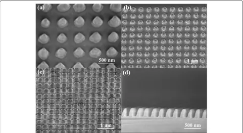
[image:2.595.57.539.431.694.2]on areas with wafer scale that is either impossible or ex-tremely time consuming with other patterning techniques. In addition, one can precisely control the geometry of the arrays in a wide range by changing the processing parame-ters such as the incident angle and exposure time. As shown in Figure 1, nanopillars with varying profiles are achieved by accurately controlling the milling conditions. One can clearly observe cone-shaped particles in Figure 1a, which were achieved by oblique milling. In Figure 1b, nor-mal round-shaped nanopillars are shown. Rough fringes are caused by redeposition which is almost inevitable in all ion-involved milling processes. Further, Figure 1c dem-onstrates nanopillars with ultrasmall separations. Note that the round shapes are replaced by quadrate outlines since the individual nanopillars are approaching each other. Smallest features of approximately 10 nm are real-ized. Figure 1d shows the cross sections of pagoda nano-pillars with high aspect ratios (100-nm average diameter and 270-nm height).
The optical properties of the fabricated nanopillars under normal incidence were measured using a commer-cial system (UV-VIS-NIR microspectrophotometer QDI 2010™, CRAIC Technologies, Inc., San Dimas, CA, USA).
A × 36 objective lens with the numerical aperture of 0.5 was employed with a 75-W xenon lamp which provided a broadband spectrum. Using a beam splitter, the partial power of the incident light beam was focused onto the sample surface through the objective lens. The spectrum acquisition for all measurements was performed with a sampling aperture size of 7.1 × 7.1 μm2. Transmission and reflection were measured with respect to the light through a bare quartz substrate and an aluminum mir-ror, respectively. To characterize the optical properties from oblique angles, an ellipsometry setup (Uvisel, Horiba Jobin Yvon, Kyoto, Japan) was employed with a broadband light source.
[image:3.595.58.539.380.697.2]Results and discussion
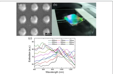
Figure 2a demonstrates the scanning electron microscopy (SEM) image of the top view of the fabricated Ag nanopil-lars with 400-nm periodicity. As can be seen, the fringe of the nanopillars presents a brighter color than the other areas due to different contrast which is caused by mate-rials redeposition during milling. Figure 2b is the optical image of nanopillars supported by a quartz substrate with the size of 1.5 × 1.5 cm2. The corners show defects caused
by fabrication imperfections since the pattern area is lim-ited during holography and uneven distribution of resist during spin coating. The extinction spectra for nanopillar arrays with varying periodicities are plotted in Figure 2c. One can clearly observe tunable LSPRs and redshift of resonance peaks with increasing periodicities. Besides, relatively large full width at half maximum can be seen for resonance peaks after 900 nm.
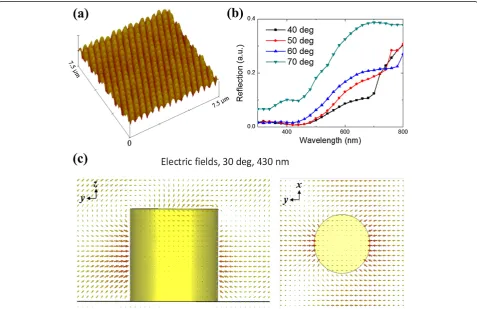
Figure 3a shows the atomic force microscopy (AFM) image of the Au nanopillar array with 450-nm periodicity. As can be seen, nanopillars with uniform shapes are achieved. The measured reflectance spectra of nanopillar arrays with different incident angles (40° to 70° in 10° increments) as a function of wavelength are plotted in Figure 3b. Tunable plasmon resonance with varying inci-dent angles can be observed. Figure 3c shows the electric near-field distribution of a single nanopillar at 30° to the incidence normal at the wavelength of 430 nm calculated by using CST microwave studio. During simulations, one unit cell was considered which consisted of a vertically oriented cylindrical Au nanopillar. Periodic boundary con-ditions were assigned to the lateral walls and Floquet ports were imposed on top and bottom of the unit cell to mimic
an infinite periodic array with a periodicity ofp= 450 nm. The nanopillar has a radius ofr= 100 nm and a height of h= 200 nm. A fifth-order Drude-Lorentz model was employed to fit the measured permittivity of Au [42]. It is observed that at the wavelength corresponding to the peak of specular reflection for each angle of incidence case, the electric field exhibits curl-like patterns, concentrating near the vertical surface of the nanopillar.
As mentioned above, Ag has a much higher etching rate than Au under the same milling parameters using ion beams. Therefore, Ag has a larger selectivity than Au with the same resist mask (fixed thickness) for milling. Figure 4a,b shows the top-view and oblique-view SEM images of Ag nanopillar arrays with ultrasmall gap sizes, respectively. The average measured smallest gap width is approximately 10 nm. Dome-shaped profiles can be ob-served from Figure 4b, which is mainly caused by mate-rials redeposition during the milling process. Note that the gaps between neighboring nanopillars have been milled through to the surface of the substrate. Typical fab-rication imperfections are highlighted with red circles.
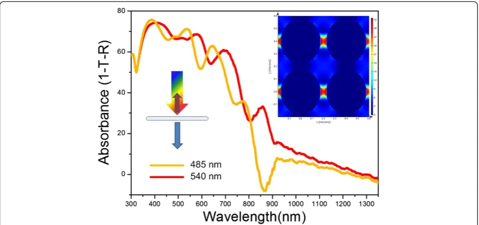
The measured absorbance spectra for two Ag nanopillar arrays with different periodicities and ultrasmall
[image:4.595.59.537.385.694.2]pillar separations are plotted in Figure 5. The LSPRs in nanopillars can be described as a series of longitudinal standing waves with an increasing number of harmonics at shorter wavelengths. In addition, the LSPRs are laterally confined and bounded between adjacent nanopillars. The spectra also show the effect of periodicity variation and re-veal different regimes. Very little radiative coupling occurs when the diffraction edge is on the high-energy side of the main LSPR since the allowed diffracted orders have higher energy than the plasmon resonance. Most of the LSPRs confined within the nanopillar array exist as higher-order modes. Note that the standing waves within the nanopillars can be influenced by the coupling of trans-verse plasmon modes between nanopillars, leading to different resonances described for separate nanopillars. Additionally, Fano-type line shapes are observed which re-sult from the interference between directly transmitted and scattered energy. Such nanopillars have great poten-tial for sensing purposes due to significantly enhanced
near-field intensity which can be clearly observed from the inset of Figure 5, possessing the key advantage of plasmonic-based sensors which may enable new oppor-tunities for sensing geometries and strategies.
Conclusions
[image:5.595.59.537.89.192.2]To conclude, we have demonstrated the fabrication of well-aligned plasmonic nanopillars by combining IL and IBM techniques. Using arrays with different geometric parameters, tunable plasmon resonances are simply achieved. It is found that Ag has a much higher milling rate than Au under the same experimental conditions, which makes Ag suitable for constructing fine nano-structures with ultrasmall features and high aspect ra-tios. The optical properties of the fabricated nanopillars are characterized both experimentally and theoretically. The approach developed in this work may trigger new applications in plasmon-assisted sensing and detecting.
[image:5.595.57.540.478.705.2]Figure 5Measured absorbance of Ag nanopillar arrays with 485- and 540-nm periodicities and 35- and 40-nm inter-pillar separations. The insets show the schematic diagram for experimental characterization at normal incidence and the electric field distribution at plasmon resonance.
Abbreviations
AFM:atomic force microscopy; IBM: ion beam milling; IL: interference lithography; IPA: isopropyl alcohol; LSPRs: localized surface plasmon resonances; SEM: scanning electron microscopy; SPs: surface plasmons; SPPs: surface plasmon polaritons.
Competing interests
The authors declare that they have no competing interests.
Authors’contributions
GS and XJ fabricated and measured the nanopillars. QG and JL helped with the simulations. FW supervised the project. All authors read and approved the final manuscript.
Acknowledgements
This work was supported by the NEU internal funding (Grant Nos. XNB201302 and XNK201406), Natural Science Foundation of Hebei Province (Grant Nos. A2013501049 and F2014501127), Science and Technology Research Funds for Higher Education of Hebei Province (Grant No. ZD20132011), Fundamental Research Funds for the Central Universities (Grant No. N120323002), Specialized Research Fund for the Doctoral Program of Higher Education (Grant No. 20130042120048), Science and Technology Foundation of Liaoning Province (Grant No. 20131031), and Scientific Research Foundation for the Returned Overseas Chinese Scholars, State Education Ministry (Grant No. 47-4).
Received: 2 May 2014 Accepted: 7 June 2014 Published: 13 June 2014
References
1. Ebbesen TW, Lezec HJ, Ghaemi HF, Thio T, Wolff PA:Extraordinary optical transmission through sub-wavelength hole arrays.Nature1998,391:667–669. 2. Liu YJ, Zheng YB, Liou J, Chiang IK, Khoo IC, Huang TJ:All-optical
modulation of localized surface plasmon coupling in a hybrid system composed of photo-switchable gratings and Au nanodisk arrays.J Phys Chem C2011,115:7717–7722.
3. Zhao Y, Nawaz AA, Lin SS, Hao Q, Kiraly B, Huang TJ:Nanoscale super-resolution imaging via metal-dielectric metamaterial lens system.J Phys D Appl Phys2011,44:41501.
4. Liu YJ, Hao QZ, Smalley JST, Liou J, Khoo IC, Huang TJ:A frequency-addressed plasmonic switch based on dual-frequency liquid crystals. Appl Phys Lett2010,97:091101.
5. Zhao Y, Lin SS, Nawaz AA, Kiraly B, Hao Q, Liu Y, Huang TJ:Beam bending via plasmonic lenses.Opt Express2010,18:23458–23465.
6. Gao H, Liu C, Jeong HE, Yang P:Plasmon-enhanced photocatalytic activity of iron oxide on gold nanopillars.ACS Nano2012,6:234–240.
7. Zhang J, Cai L, Bai W, Song G:Hybrid waveguide-plasmon resonances in gold pillar arrays on top of a dielectric waveguide.Opt Lett2010, 35:3408–3410.
8. Wang K, Crozier KB:Plasmonic trapping with a gold nanopillar. ChemPhysChem2012,13:2639–2648.
9. Cetin AE, Yanik AA, Yilmaz C, Somu S, Busnaina A, Altug H:Monopole antenna arrays for optical trapping, spectroscopy, and sensing.Appl Phys Lett2011,98:111110.
10. Kubo W, Fujikawa S:Au double nanopillars with nanogap for plasmonic sensor.Nano Lett2011,11:8–15.
11. Kabashin AV, Evans P, Pastkovsky S, Hendren W, Wurtz GA, Atkinson R, Pollard R, Podolskiy VA, Zayats AV:Plasmonic nanorod metamaterials for biosensing.Nat Mater2009,8:867–871.
12. Chigrin D, Lavrinenko A, Torres CS:Numerical characterization of nanopillar photonic crystal waveguides and directional couplers. Opt Quant Electron2005,37:331–341.
13. Zhao Y, Gan D, Cui J, Wang C, Du C, Luo X:Super resolution imaging by compensating oblique lens with metallodielectric films.Opt Express2008, 16:5697–5707.
14. Melville DOS, Blaikie RJ:Super-resolution imaging through a planar silver layer.Opt Express2005,13:2127–2134.
15. Casse BDF, Lu WT, Huang YJ, Gultepe E, Menon L, Sridhar S:Super-resolution imaging using a three-dimensional metamaterials nanolens.Appl Phys Lett 2010,96:023114.
16. Cao T, Wang S:Topological insulator metamaterials with tunable negative refractive index in the optical region.Nanoscale Res Lett2013, 8:526.
17. Cai W, Chettiar UK, Kildishev AV, Shalaev VM:Optical cloaking with metamaterials.Nat Photon2007,1:224–227.
18. Chen H, Chan CT:Acoustic cloaking in three dimensions using acoustic metamaterials.Appl Phys Lett2007,91:183518.
19. Xue J, Zhu Q, Liu J, Li Y, Zhou ZK, Lin Z, Yan J, Li J, Wang XH:Gold nanoarray deposited using alternating current for emission rate-manipulating nanoantenna.Nanoscale Res Lett2013,8:295.
20. Aubry A, Lei DY, Fernández-Domínguez AI, Sonnefraud Y, Maier SA, Pendry JB:Plasmonic light-harvesting devices over the whole visible spectrum. Nano Lett2010,10:2574–2579.
21. Cole JR, Halas NJ:Optimized plasmonic nanoparticle distributions for solar spectrum harvesting.Appl Phys Lett2006,89:153120.
22. Si G, Zhao Y, Liu H, Teo S, Zhang M, Huang TJ, Danner AJ, Teng JH:Annular aperture array based color filter.Appl Phys Lett2011,99:033105. 23. Liu YJ, Si GY, Leong ESP, Xiang N, Danner AJ, Teng JH:Light-driven
plasmonic color filters by overlaying photoresponsive liquid crystals on gold annular aperture arrays.Adv Mater2012,24:OP131–OP135. 24. Si G, Zhao Y, Lv J, Lu M, Wang F, Liu H, Xiang N, Huang TJ, Danner AJ, Teng
J, Liu YJ:Reflective plasmonic color filters based on lithographically patterned silver nanorod arrays.Nanoscale2013,5:6243–6248. 25. Si G, Zhao Y, Leong ESP, Liu YJ:Liquid-crystal-enabled active plasmonics:
a review.Materials2014,7:1296–1317.
26. Zhao Y, Hao Q, Ma Y, Lu M, Zhang B, Lapsley M, Khoo IC, Huang TJ: Light-driven tunable dual-band plasmonic absorber using liquid-crystal-coated asymmetric nanodisk array.Appl Phys Lett2012,100:053119.
27. Zhang B, Zhao Y, Hao Q, Kiraly B, Khoo IC, Chen S, Huang TJ:Polarization independent dual-band infrared perfect absorber based on a metal-dielectric-metal elliptical nanodisk array.Opt Express2011, 19:15221–15228.
28. Liu N, Mesch M, Weiss T, Hentschel M, Giessen H:Infrared perfect absorber and its application as plasmonic sensor.Nano Lett2010,10:2342–2348. 29. Fan Z, Kapadia R, Leu PW, Zhang X, Chueh YL, Takei K, Yu K, Jamshidi A,
Rathore AA, Ruebusch DJ, Wu M, Javey A:Ordered arrays of dual-diameter nanopillars for maximized optical absorption.Nano Lett2010, 10:3823–3827.
30. Caldwell JD, Glembocki O, Bezares FJ, Bassim ND, Rendell RW, Feygelson M, Ukaegbu M, Kasica R, Shirey L, Hosten C:Plasmonic nanopillar arrays for large-area, high-enhancement surface-enhanced Raman scattering sensors.ACS Nano2011,5:4046–4055.
31. Senanayake P, Hung CH, Shapiro J, Scofield A, Lin A, Williams BS, Huffaker DL:3D nanopillar optical antenna photodetectors.Opt Express2012, 20:25489–25496.
32. Caldwell JD, Glembocki O, Bezares FJ, Kariniemi MI, Niinisto JT, Hatanpaa TT, Rendell RW, Ukaegbu M, Ritala MK, Prokes SM, Hosten CM, Leskela MA, Kasica R:Large-area plasmonic hot-spot arrays: sub-2 nm interparticle separations with plasma-enhanced atomic layer deposition of Ag on periodic arrays of Si nanopillars.Opt Express2011, 19:26056–26064.
33. Tsai SJ, Ballarotto M, Romero DB, Herman WN, Kan HC, Phaneuf RJ:Effect of gold nanopillar arrays on the absorption spectrum of a bulk
heterojunction organic solar cell.Opt Express2010,18:A528–A535. 34. Lin HY, Kuo Y, Liao CY, Yang CC, Kiang YW:Surface plasmon effects in the
absorption enhancements of amorphous silicon solar cells with periodical metal nanowall and nanopillar structures.Opt Express2012, 20:A104–A118.
35. Zeng B, Gao Y, Bartoli FJ:Ultrathin nanostructured metals for highly transmissive plasmonic subtractive color filters.Sci Rep2013,3:2840. 36. Zeng B, Yang X, Wang C, Luo X:Plasmonic interference nanolithography
with a double-layer planar silver lens structure.Opt Express2009, 17:16783–16791.
37. Zeng B, Gan Q, Kafafi ZH, Bartoli FJ:Polymeric photovoltaics with various metallic plasmonic nanostructures.J Appl Phys2013,113:063109. 38. Zeng B, Yang X, Wang C, Feng Q, Luo X:Super-resolution imaging at
different wavelengths by using a one-dimensional metamaterial structure. J Opt2010,12:035104.
40. Xu T, Fang L, Zeng B, Liu Y, Wang C, Feng Q, Luo X:Subwavelength nanolithography based on unidirectional excitation of surface plasmons. J Opt A Pure Appl Opt2009,11:085003.
41. Drezet A, Koller D, Hohenau A, Leitner A, Aussenegg FR, Krenn JR: Plasmonic crystal demultiplexer and multiports.Nano Lett2007, 7:1697–1700.
42. Johnson PB, Christy RW:Optical constants of the noble metals.Phys Rev B 1972,6:4370–4379.
doi:10.1186/1556-276X-9-299
Cite this article as:Siet al.:Fabrication and characterization of well-aligned
plasmonic nanopillars with ultrasmall separations.Nanoscale Research Letters
20149:299.
Submit your manuscript to a
journal and benefi t from:
7Convenient online submission
7Rigorous peer review
7Immediate publication on acceptance
7Open access: articles freely available online
7High visibility within the fi eld
7Retaining the copyright to your article