Synchrotron radiation studies of
organic/inorganic semiconductor
interfaces
A thesis submitted to
THE UNIVERSITY OF DUBLIN
for the degree of
Doctor in Philosophy
Grégory Cabailh
Department of Physics
University of Dublin, Trinity College
Dublin 2, Ireland
Declaration
This thesis is submitted by the undersigned to The University of Dublin for the examination for the degree of Doctor in Philosophy.
This thesis has not been submitted as an exercise for a degree to any other university.
With the exception of the assistance noted in the acknowledgements, this thesis is entirely my own work.
I agree that the Library of The University of Dublin may lend or copy this thesis upon request.
--- Grégory Cabailh
Abstract
on both substrates. The spectra show that the films are highly orientated. At a monolayer level, the molecules are lying close to flat on the substrate surface. For thick films, it is clear that each molecule exhibits a different orientation in the films, e.g. SnPc lying close to flat to the surface whereas MgPc is ‘standing up’. The molecules exhibit the same behaviour on both substrates. By analysing the evolution of the π* resonance intensity, the possible crystalline structures were also deduced.
Acknowledgments
Firstly, I would like to thank my supervisor Prof. Iggy Mc Govern for his support and his advice throughout my studies. I would also like to thank Dr. Andrew Evans from the University of Wales, Aberystwyth for the time he has allocated me at synchrotron radiation sources and for all the helpful discussions. I am very grateful to Dr. Tony Cafolla from Dublin City University for the extended use of the STM system and to Philippe Guéno for his help and advice on that system. I would especially like to thank Alex for all the discussions, help at synchrotron radiation sources and for putting up with me during the long night shifts!
I am also grateful to Adam, Joachim, Tom, Colm, Céline, Bastien, for their help and collaboration and who contributed to the success of the beamtimes. I would to thank Simon, Lee and Justin for their help in the lab and the good atmosphere they created. I will also thank everybody, especially Ken, Emma and James, who made my PhD years in Dublin a very enjoyable time and Ken again for his guaranteed availability for the coffee breaks!
I will also acknowledge the support of beamline coordinators, Dr V R Dhanak and George at the SRS and Dr C Crotti and colleagues at Elettra.
Chapter 1 Introduction
……… 11Chapter 2 Theory
……… 152.1. Inorganic semiconductor substrates ……… 15
2.1.1. Germanium (001) ……… 15
2.1.2. Gallium arsenide (001) ……… 16
2.2. Metal Phthalocyanines ……… 18
2.2.1. Molecular structure ……… 19
2.2.2. Crystalline structure ……… 20
2.2.2.1. Planar phthalocyanines, structure of the monoclinic α and β form ……… 20
2.2.2.2. Non-planar phthalocyanine ……… 21
2.2.2.2.1. SnPc and PbPc triclinic form …… 21
2.2.2.2.2. PbPc monoclinic form …… 22
2.2.3. Multilayer growth on substrate ……… 23
2.2.3.1. Planar phthalocyanines ……… 23
2.2.3.2. Non-planar phthalocyanines ……… 25
2.2.4. Monolayer structure ……… 26
2.3. Characterisation techniques ……… 28
2.3.1. Photoemission spectroscopy (PES) ……… 28
2.3.1.1. Basic concepts ……… 29
2.3.1.2. Theoritical background ……… 31
2.3.1.2.1. Interaction of light with matter …… 31
2.3.1.2.2. Evaluation of the photoemission transition probability ……… 33
2.3.1.2.3. Electric dipole selection rules …… 35
2.3.1.2.4. The three-step and the one-step models 35 2.3.1.2.5. Symmetry of wavefunctions …… 40
2.3.1.3. Concentric hemispherical analyser (CHA) …… 40
2.3.1.4. Core level shift spectroscopy ……… 43
2.3.1.5. Growth mode ……… 45
2.3.2. Near edge x-ray fine structure (NEXAFS) ……… 50
2.3.3. Low energy electron diffraction (LEED) ……… 55
2.3.4. Auger electron spectroscopy (AES) ……… 57
2.3.5. Scanning tunnelling microscopy (STM) ……… 59
Chapter 3 Experimental details
……… 623.1. Substrate preparation ……… 62
3.1.1. LEED and AES ……… 63
3.1.2. STM, Dublin City University ……… 65
3.2. Organic film deposition ……… 66
3.3. Synchrotron radiation ……… 67
3.4.1. SRS Daresbury, beamline 4.1 ……… 68
3.4.2. SRS Daresbury, beamline 1.1 ……… 69
3.4.3. Elettra, VUV beamline ……… 69
3.4.4. ASTRID, SGM1 beamline ……… 70
3.4.5. MAX-lab, beamline 41 ……… 70
3.4. Curve fitting ……… 71
Chapter 4 Core level spectroscopy
……… 744.1. Substrate surfaces ……… 74
4.1.1. GaAs(001)-1×6 ……… 75
4.1.2. Ge(001)-2×1 ……… 77
4.2. Molecules deposited on GaAs(001)-1×6 ……… 79
4.2.1. SnPc ……… 79
4.2.1.1. Ga3d and As3d core levels ……… 79
4.2.1.2. Sn4d core level ……… 81
4.2.2. PbPc ……… 81
4.2.2.1. Ga3d and As3d core levels ……… 81
4.2.2.2. Pb5d core level ……… 83
4.2.3. MgPc ……… 83
4.2.3.2. Mg2p core level ……… 85
4.2.4. Conclusion ……… 85
4.3. Molecules deposited on Ge(001)-2×1 …...………. 86
4.3.1. SnPc ……… 86
4.3.1.1. Ge3d core level ……… 86
4.3.1.2. Sn4d core level ……… 87
4.3.2. PbPc …………...………. 88
4.3.2.1. Ge3d core level ……… 88
4.3.2.2. Pb5d core level ……… 90
4.3.3. MgPc ……… 90
4.3.3.1 Ge3d core level ……… 90
4.3.2.2. Mg2p core level ……… 92
4.3.4. Conclusion ……… 92
4.4. Comparison of GaAs and Ge substrates ……… 94
4.5. Annealing of thick organic layers ……… 95
4.6. Beam damage ……… 97
Chapter 5 Valence band spectroscopy and energetics
99 5.1. Valence band spectroscopy ……… 995.2. Energetics ……… 101
5.3. Beam damage ……… 105
Chapter 6 Film growth mode
……… 1086.1. PbPc growth mode ……… 108
6.2. MgPc growth mode ……… 109
6.2.1. MgPc deposited on Ge(001)-2×1 ……… 109
6.2.2. MgPc deposited on GaAs(001)-1×6 ……… 110
6.3. SnPc growth mode ……… 111
6.3.1. SnPc deposited on Ge(001)-2×1 ……… 111
Chapter 7 Molecular orientation
……… 1147.1. MgPc ……… 115
7.1.1. MgPc deposited on Ge(001)-2×1 ……… 115
7.1.2. MgPc deposited on GaAs(001)-1×6 ……… 116
7.1.3. Summary of MgPc NEXAFS ……… 116
7.1.4. STM of a submonolayer of MgPc on Ge(001) …… 117
7.2. SnPc ……… 118
7.2.1. SnPc deposited on Ge(001)-2×1 ……… 118
7.2.2. SnPc deposited on GaAs(001)-1×6 ……… 120
7.2.3. Summary of SnPc NEXAFS ……… 121
7.3. PbPc deposited on Ge(001)-2×1 ……… 122
7.4. Overall conclusions ……… 123
Chapter 8 Conclusions
……… 125References
……… 129Chapter 1 Introduction
In recent years a lot of work has been done trying to improve electronic devices. Organic materials have been of great industrial interest since they can be easily prepared and are much cheaper than inorganic semiconductors. Organic electronic materials have shown to be very suitable components for a wide range of applications such as photovoltaic cells [1], organic light emitting diodes (OLED’s) [2-6], molecular electronics, biological recognition and chemical sensors [7, 8], organic field-effect transistors [9-16] and electronic signal rectifiers and amplifiers [17]. They are also used as switching devices for active displays. In addition, OLED displays show a wide viewing angle and a broad temperature range at low power consumption. Efficiency and the extent of colours of OLEDs are of the order of inorganic based diodes [13].
Due to the wide range of organic molecules, organic thin films can be used to change and tune the properties of electronic devices such as Schottky diodes, designing them for specific applications [18]. These heterojunctions have been widely studied in the recent years [19-30]. Investigations into the applications of these materials in the field of telecommunications include the potential for the use of organic thin films active layers in epitaxially grown hybrid organic-inorganic devices. By introducing thin films of 3,4,9,10-perylenetetracarboxylic dianhydride (PTCDA) in hybrid Ag/PTCDA/InP [3], the effective barrier height can be varied depending on the PTCDA layer thickness. An estimate of 42 GHz is given for the high frequency limit for an optimised InP device which is about one third of the frequencies obtained in nowadays commercially available GaAs Schottky diodes.
the organic film. The principal technique is photoemission spectroscopy, using synchrotron radiation, supplemented with NEXAFS.
(v) The Overall Device Performance
GaAs(100)
Organic Interlayer Metal
V
I
(iv) The Interface between the
OrganicMolecules and the metal
(iii) The Organic
Molecular Film
(ii) The Interface between
GaAs Substrate and OrganicMolecules
(i) The GaAsSubstrate Surface
(v) The Overall Device Performance
GaAs(100) Organic Interlayer Metal V I GaAs(100) Organic Interlayer Metal V I
(iv) The Interface between the
OrganicMolecules and the metal
(iii) The Organic
Molecular Film
(ii) The Interface between
GaAs Substrate and OrganicMolecules
(i) The GaAsSubstrate Surface
Fig. 1.1. Organic modified Schottky contacts and principal components for the characterisation
The starting point of this work is the inorganic semiconductor surface. Surface properties, which can be quite different from bulk properties, play a vital role in the performance of electronic components so it is very important to study the electronic properties at the interface to get a full understanding. Also the deposition of organics may depend on the properties of the surface. Thus we need to investigate the reconstruction and properties of the clean surface.
The initial stages of formation of such an organic/inorganic interface can be followed by surface sensitive soft x-ray photoelectron spectroscopy (SXPS), with organic molecular beam deposition (OMBD) providing good control of depositing conditions. The molecule-substrate interaction has an important role for the first monolayer morphology. For subsequent layers, the structure is determined by the molecule-molecule interaction; in that case the role of the substrate is to define a plane of reference.
In the organic-based heterostructures the metal/organic and organic/inorganic interfaces play a role but the structure of the organic films is essential in determining the transport properties. In particular, the polycrystalline nature of organic films [2] may be a limiting factor for the carrier mobilities. In this work, the film structure is investigated in two ways: first the growth mode, secondly the molecular orientation within the film.
Gallium arsenide is mainly used in this work since it was the substrate of choice in the DIODE network. To widen the scope, germanium was also used as a substrate. It is monoatomic, has a different reactivity and provides a more reproducible surface. It is also well characterised in the literature. The molecules of choice were metal phthalocyanines: SnPc, PbPc and MgPc. These molecules were chosen firstly because they have a low vapour pressure. Secondly, the central metal atom can be easily tracked by photoemission spectroscopy. And thirdly they are different in shape.
Chapter 2 Theory
Firstly, the substrates structure of the Ge(001)-2×1 and GaAs(001)-1×6 surface reconstructions are explained. Secondly, the metal phthalocyanine molecules and their crystalline structure are described with a distinction between planar and non-planar molecules. In a third part an introduction to the experimental techniques used to characterise the organic/inorganic interface and the thin films is made.
2.1. Inorganic semiconductor substrates
2.1.1. Germanium (001)
Germanium is a group-IV semiconductor with a bulk crystal structure consisting of two interpenetrating face-centered cubic primitive lattices, also known as the diamond structure (figure 2.1a). It has a band-gap of 0.67 eV at 300 K and a Ge-Ge bulk bond length of 2.45 Å. The (001) and equivalent planes correspond to the faces of the unit cell.
(a) (b)
Fig. 2.1. (a) Bulk diamond structure of crystalline germanium. Each atom has an sp3 hybridisation and is
On an ideally truncated Ge(001) surface, each surface atom possesses two dangling bonds (figure 2.1b). To minimise the surface free energy, atoms at the surface will reorganise. The reconstruction of the Ge(001) surface is based upon the ‘dimerisation’ of surface atoms. Two nearest neighbours Ge atoms pair together creating dimers. The number of dangling bond is then reduced by a factor of two. This reduces the free surface energy due to the stability gained by creating a chemical bond outweighing that lost from strain. Each Ge surface atoms has four valence electrons, two of which are used in bonding to Ge atoms in the second layer; a third one is used in the formation of the dimer (dimer length: 2.46 Å [36] and 2.55 Å [37]). This leaves one electron in the dangling bond per Ge surface atom. However, this configuration is unstable, leading to a tilt out of the surface plane of the surface dimers (figure 2.1b) [36, 38-40]. The dimers are tilted by 10° to 20°. This induces a significant transfer of electronic charge from the recessed atom (or ‘‘down atom’’) to the protruding atom (or ‘‘up atom’’) [41]. Consequently, the down atom is electrophilic and the up atom is nucleophilic [42].
There are two stable arrangements at low temperature: the c(4x2) and p(2x2) reconstructions [43-46]. The tilting of the dimers alternates down the rows, the latter being separated by trenches. For the c(4x2) reconstruction, the dimers are buckled in opposite orientations in adjacent rows whereas they are buckled in the same direction for the p(2x2) surface. The c(4x2) reconstruction is considered to be the ground state [47-49]. At room temperature a 2x1 reconstruction is observed which is believed to be due the ‘flipping’ of the unstable Ge-Ge dimers [37, 46, 50]. But the c(4x2) and p(2x2) reconstruction can also be seen at room temperature due to the ‘freezing’ of the dimers by defects or step edges. Although the number of dangling bonds is reduced by the reconstruction, Ge(001)-2×1 is still highly reactive and sticking probabilities of many organic molecules are near unity at room temperature [51].
2.1.2. Gallium Arsenide (001)
table. It has a direct bandgap of 1.42 eV at 300 K. The ideal (001) surface is polar. Thus the top layer would consist of either arsenic anions or gallium cations. GaAs(001) surfaces are, in practice, not ideally terminated and they exhibit a number of different reconstructions and stoichiometry depending on sample preparation [52-55]. The lattice of a tetrahedrally coordinated III-V semiconductor has only a two fold symmetry about the [001] axis and therefore cation (Ga) dangling bonds will always lie along the [011] direction and the anion (As) dangling bonds along the [01 ] [56]. Diffraction patterns 1 of reconstructions with ×6 symmetry can result from a superposition of two or more
local phases. For example, it has been reported that the 4×6 reconstruction is a
combination of the 4×1 and 1×6 phases [53, 57]. In the case of the 1×6 reconstruction
obtained by argon sputtering and annealing [53, 54, 57], three surface reconstructions have been proposed (figure 2.2).
Biegelsen et al [52] Chizov et al [58] Kuball et al [59]
Fig. 2.2. Structural models for the GaAs(001)-1×6 surface proposed by Biegelsen et al (left), Chizhov et
al (middle) and Kuball et al (right).
Biegelsen et al [52] have proposed a model for the ‘2×6’ model consisting of two As
dimers and four missing As dimers stacked along the x6 direction (i.e. the [011]
dimer-atoms in the next layer (described as a trench) with the row separation of 24 Å. The four As dimer-atoms are bonded to six Ga atoms, of which four have non-bulk environments. The streaks observed on the LEED pattern are due to the stacking
disorder in the [01 ] direction. The model of Chizhov et al [58] retains the trench but 1
suggests a more complicated arrangement between the trenches, an idealised 12x6 unit cell. The 2x6 rows exhibit a certain degree of disorder which suggests that the As dimers do not have a unique arrangement suggesting that it is a transition phase. A third model was also proposed by Kuball et al [59], where the top-layer consists of regular two-As-dimer rows and the x6 comes from the missing dimer row. The structure of the GaAs(100)-1x6 is reported to be a transition structure and many stoichiometries have been reported [53, 54, 57]. Thus there might not be a unique model for this surface reconstruction.
2.2. Metal Phthalocyanines
A wide range of organic molecules is available for thin film deposition. Among the many studies on organic molecule adsorption two main types have emerged so far – perylenes derivatives (e.g. PTCDA, PTCDI) and metal phthalocyanines. In this work, the molecules of choice were metal phthalocyanines: SnPc, PbPc, MgPc. These molecules were chosen for the possible tracking of the central metal atom and for the difference in their shape (see next section). Phthalocyanines have a low vapour pressure (10-14 torr) suitable for UHV sublimation and in-situ experiments. They are semiconducting, thermally stable and high purity can be obtained. There is no noticeable degradation in air up to 400-500°C. They are also chemically stable. Only with very strong oxidising agents can the molecules be broken down to phthalimide or
phthalic acid [60, 61].
2.2.1. Molecular structure
Metal phthalocyanines, MC32H16N8, are symmetrical macrocycle molecules composed
of four benzene pyrrole groups (isoindole groups) connected together by four meso-bridging aza nitrogens. The structure has a central cavity of sufficient size to accommodate various metal ions (up to 70 metal phthalocyanines have been reported), which are bonded to the pyrrole nitrogens (figure 2.3). They exhibit aromatic behaviour due to the delocalised electron density of the π-bonds above and below the plane of the molecules. The choice of the central atom can influence the physical properties of the molecule [62]. The metal is usually in a 2+ oxidation state and the macrocycle backbone usually exists as a dianion (Pc2-). The molecule is planar for low Z central atoms and has a four-fold rotation axis, i.e. belonging to the D4h point group. MgPc is an example
of this type.
SnPc
PbPc
Fig. 2.3. Top view of a planar phthalocyanine metal complex (left). Side view of the SnPc (top right) and PbPc (bottom right) are also represented, courtesy of Seán M. O'Flaherty. Carbon, nitrogen and hydrogen atoms are represented in light blue, dark blue and grey respectively.
In the case of SnPc and PbPc, the size of the central metal atom induces the molecule to depart from a planar geometry resulting in a steric effect protrusion [63]. The molecules exhibit a ‘shuttlecock’ shape. This suppresses the horizontal plane of symmetry and thus the molecules belong to the C4v point group. The protrusion of the Pb atom varies
in the triclinic phase. This is due to the intermolecular interactions within the crystalline film.
2.2.2. Crystalline structure
The crystalline structure of metal phthalocyanines is complex and there are many different structures depending on the molecule (i.e. shape, ligands). Also forces within these organic films are weak, thus there are different possible crystalline forms for a specific metal phthalocyanine. They have been extensively studied and some good reviews have been published [62, 64-66].
For metal phthalocyanines with no side or axial ligand, the molecules can be separated into two distinguishable types, planar and non-planar. MgPc belongs to the former type whereas SnPc and PbPc belong to the latter.
2.2.2.1. Planar phthalocyanines, structure of the monoclinic αααα and ββββ form
The structure of planar phthalocyanines crystals was first investigated by X-ray diffraction [67, 68]. For planar phthalocyanines (e.g. CuPc, MgPc) there are two main
crystalline forms, the α and β forms (figure 2.4) [62]. They differ from one another in
the degree of tilt within the columnar stacks. The angle of tilt of the plane of the
molecule is between 25° and 28° with respect to the a-axis of the crystal for the α-form
and between 45° and 48° for the β-form. Both are of the monoclinic structure (i.e.
a≠b≠c and α=γ=90°≠β). The molecules in neighbouring stacks in the β-form are nearly
orthogonal producing a ‘herringbone arrangement’. The β-form is the most
thermodynamically stable polymorph for planar phthalocyanines. Other crystalline
forms such as the X-form have also been reported. Annealing the α-form converts it
Fig. 2.4. Schematic showing the columnar stacking of the α-phase (top) and β-phase (bottom) for planar
Pcs [65]. The data shown refer to the cell parameters for CuPc. Both phases are monoclinic. The α-phase
has four molecules in the unit cell, the β-phase has two.
2.2.2.2. Non-planar phthalocyanines
Non-planar phthalocyanines exhibit a different behaviour. SnPc and PbPc have been reported to grow in a triclinic structure [72, 73]. There is also another crystalline form for PbPc, the monoclinic form [74].
2.2.2.2.1. SnPc and PbPc triclinic form
For PbPc, the molecules are tilted 59.9° with respect to the plane perpendicular to the stacking axis. In this crystallographic form the Pb2+ ions are 6.42 Å and 8.33 Å apart and the d.c. conductivity is 10-10 Sm-1. Such differences between the two forms make it important to understand and control film growth for electronic applications. SnPc is not as widely studied as PbPc. In this material, the angle of tilt of the molecules with respect to the plane perpendicular to the stacking axis is estimated from crystallographic data [64] to be 50°.
a-axis a-axis
Fig. 2.5. SnPc (left) and PbPc (right) triclinic crystalline structures. The top row is a view with the stacking axis in the plane of the sheet. The bottom row is a side view of the molecules stacking within a column. Reproduced from [64].
2.2.2.2.2. PbPc monoclinic form
Fig. 2.6. Monoclinic crystalline structure of lead phthalocyanine adapted from [72]
2.2.3. Multilayer growth on a substrate
The crystalline form of a phthalocyanine film is dependent of the central atom (i.e. planar or non-planar molecules), on the rate of deposition and on the substrate [76]. The temperature at which the substrate is held during deposition also has an important role. Higher substrate temperatures yield rough films composed of micro-crystallites [77] and different crystalline forms can be obtained [78]. A key issue for this thesis is the orientation of a given crystallite relative to the plane of the substrate but this is not always available in the literature. Where possible, this is discussed in terms of the main stacking crystalline axis. The planar and non-planar types are discussed separately.
2.2.3.1. Planar phthalocyanines
Films deposited at room temperature are mainly of the α-form [70, 71, 79, 80].
However different orientations of the crystallites relative to the substrate have been
observed. These possibilities are summarised in figure 2.7. Highly ordered α-form thin
orientation of the α-form where one molecule out of two lies parallel to the surface
(model b). Yamada et al [79] proposed a model where all the molecules are lying flat on
the surface (model c). Finally, Hassan et al [69] reported brush-like α-form crystallites
for thick films grown on substrate at room temperature with the crystallographic b-axis perpendicular to the substrate (model d).
Fig. 2.7. Schematic of plausible growth of a film of planar MPc (a) with the columnar axis (i.e. the b-axis) parallel to the surface; (b) where one out of two molecules is parallel to the surface as proposed by Ashida et al; (c) growth with all the molecules parallel to the surface; (d) vertical columnar growth with the b-axis perpendicular to the surface. Reproduced from [65].
The molecular orientation within the film can also be dependent on the quality of the substrate. Peisert et al report that CuPc appears to ‘lie flat’ on ordered surfaces but ‘stands up’ on rough surfaces [76]. However they do not give a more precise relation
2.2.3.2. Non-planer Pc
Previous studies have concentrated almost exclusively on PbPc. To our knowledge there is no literature for SnPc in which crystal orientation with respect to the substrate surface has been reported. The following review therefore concerns only PbPc.
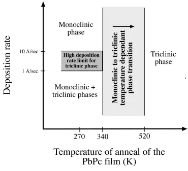
The type of crystalline form obtained depends on the temperature of the substrate. Generally, the monoclinic crystalline form is obtained on samples at room temperature. Higher substrate temperatures favour the triclinic form [78].
The crystalline form also depends on the deposition rate. However the boundary is not quite clear. Miyamoto et al [78] obtained mainly monoclinic crystalline form for rates greater than 1.0 nm.s-1 and a mixture of both forms for lower rates. Ottaviano et al [83] have reported mainly monoclinic phase with a deposition rate as low as 0.02 nm.s-1 and a substrate kept at room temperature. Again, a mixture of monoclinic and triclinic form
is obtained for lower deposition rates.
Ottaviano et al [83] have reported mainly monoclinic phase with the c-axis parallel to the substrate. After annealing at 170°C, they observe the triclinic form with the a-axis parallel to the substrate whereas the remaining monoclinic phase rotates such that the c-axis is perpendicular to the substrate. Myamoto et al [78] also observe the two orientations for the monoclinic phase. They also obtain a mainly triclinic film when the substrate is held at 100°C. They observe a triclinic structure for low deposition rates and when the substrate is kept at room temperature; however, in this paper the orientation with respect to the substrate is not explicitly defined. Collins et al [84] observe a mixture of monoclinic and amorphous phase deposited on substrates held at room temperature; again, the orientation relative to the substrate is unavailable.
films deposited on silicon. This transition was reported to start between 50° and 70°C [86].
Fig. 2.8. Phase diagram of the monoclinic and triclinic phase of PbPc depending on the deposition rate and the annealing temperature of the organic film. Different temperatures have been reported in the literature for the transition from the monoclinic to the triclinic phase. The light dotted area represents this transition. Similarly different deposition rates at which the triclinic phase appears have been reported. This is represented by the dark filled region.
2.2.4. Monolayer structure
[image:26.595.124.494.145.482.2]The archetype molecules studied to date are CuPc and PbPc. CuPc presumably is a reasonable model for MgPc; PbPc presumably is a reasonable model for SnPc.
[image:27.595.150.479.257.509.2]Copper phthalocyanine has been shown to form a well ordered initial layer on reactive metallic and semiconductor surfaces [33, 35, 83, 87-91]. Cox et al report that on the In-terminated (001) and (111) surfaces of InSb and InAs, CuPc molecules lie flat on the surface and are commensurate with the substrate structures [21, 33].
Fig. 2.9. Adsorption model of PbPc on c(8×2)-InSb(100) reconstruction [92]
Forrest et al [93] showed by RHEED that the first layer of PbPc molecules lie flat with a square commensurate lattice on KBr(001), NaCl(001) and KCl(001). Non-planar
phthalocyanines such as PbPc raise a further issue as to which side of the molecule is towards the substrate. STM studies from Papageorgiou et al show that PbPc molecules are commensurate with the surface and that they lie flat on InSb but with the Pb atom towards the substrate (see figure 2.9) [94]. STM studies from Strohmaier et al [35] suggest that PbPc lies flat on the basal face of MoS2; the molecules can adopt three
also report both possible adsorption geometries i.e. the Pb lying towards and away from the surface.
The common theme of the above studies is that the molecules lie flat on the substrate. However, these techniques may not distinguish a small angle of tilt with respect to the substrate, as is known to occur for thicker films.
2.3. Characterisation techniques
The two main techniques used in this work are photoemission spectroscopy and near-edge x-ray absorption fine structure (NEXAFS). Photoemission spectroscopy is a good technique to monitor the interaction between the substrate and the adlayer. It is also an indirect monitor of the growth mode of thin films. It is possible to find the molecule orientation on a substrate or within thin films using NEXAFS. A limited access to
scanning tunnelling microscopy enabled a preliminary investigation of the orientation of the molecules for submonolayers with respect to the substrate.
2.3.1. Photoemission spectroscopy
Photoemission spectroscopy is based on the photoelectric effect discovered by Hertz in 1887 and explained in 1905 by Einstein when he introduced the quantum theory of photoemission. In the 1960’s, Kai Siegbahn (Nobel prize winner 1981) at the University of Uppsala significantly developed the technique as a tool for chemical analysis.
Spectroscopic techniques use interactions between photons and matter to probe the electronic structure and measure thereby the energy distribution of electronic states in atoms, molecules or solid states materials. Depending on the energy of light source, PES is divided into ultraviolet (UPS), soft X-ray (SXPS), and X-ray photoemission spectroscopy (XPS). UPS is commonly used to study states near the Fermi level EF, in
utilising synchrotron radiation (SXPS) both valence band and core levels can be probed in a simple experiment.
2.3.1.1. Basic concepts
hu F e rm i le v e l hu D e n s it y o f s ta te s 0 C u t o ff , E v a c F e rm i le v e l Core levels Core levels ValenceBand
Valence Band
Kinetic energy
Fig 2.10. Schematic energy level diagram relating the atomic levels to the measured spectrum for an
electron emitted in vacuum with a photon energy hu. The right part of the diagram is a schematic of the
valence band and the core levels. The right hand side shows the resulting photoemission spectrum.
In PES, the surface of a sample is irradiated with monochromatised light of energy hu, which causes photoionisation of atoms in the sample. In the ‘one-electron’ model, if the incident photon is of sufficient energy to ionise an atom then the ejected photoelectron will have a kinetic energy (Ekin) which is characteristic of its energy state for a given photon energy (Eq. 2.1).
Ekin = hu - EB - φ (Eq. 2.1)
Synchrotron radiation is the electromagnetic radiation emitted when a charge moving at relativistic speeds in a storage ring follows a curved trajectory [95]. This radiation represents the main energy loss mechanism for particles so constrained. The light is emitted in a continuous spectrum from infrared to hard x-rays in a very narrow cone tangential to the electron orbit. It is strongly collimated in the forward direction and strongly polarised in the plane of the storage ring (see figure 2.11).
Fig. 2.11. Schematic of a synchrotron radiation source
pulsed time structure (i.e. at the SRS Daresbury a pulse is seen every 2 ns in multibunch mode).
The flux of synchrotron radiation can be enhanced using undulators or wigglers instead of bending magnets. In a wiggler or an undulator, electrons travel through a periodic magnetic structure. In an undulator constructive interference is achieved between light pulses emitted at different magnets generating a narrow cone of light at a characteristic frequency and 100% polarised in the plane of the ring. In a wiggler, the interference effects are less important and radiation from different parts of the electron trajectory adds incoherently. In this work, bending magnet and undulator beamlines were used.
In the normal experimental set up a monochromator is placed between the ring and the experimental chamber allowing a narrow range of photon energy to be selected. In this lies the main advantage of the synchrotron over the lab sources. By varying the photon energy it is possible to use the corresponding change in the photoelectron mean-free
path to achieve maximum surface sensitivity. Other useful properties are high photon flux and strong polarisation.
2.3.1.2. Theoretical background
2.3.1.2.1. Interaction of light with matter
In non-relativistic quantum mechanics [97] the electromagnetic radiation field A is a vector potential operator at position ri and time t,
,
i i † i i
, c
V ˆ ˆ
( , ) e e
2 k
k r k r
k k
A A r a a
α
⋅ − ⋅ +
α α α
α
= =
∑∑
ε i ωt + ε i ωt iω
t h (Eq. 2.2)
where ak,αand ,
†
α
k
a are annihilation and creation operators, which decrease and increase
frequency. For the electron of an atom in a quantum mechanical system describing some material, the interaction Hamiltonian can be written as:
(
)
22 2
int
H = e A p p A⋅ + ⋅ − φ +e e A A⋅
mc mc (Eq. 2.3)
where φ is the scalar potential of the incident light field, e is the electron charge and m its rest mass. Following the Green function approach, the photocurrent within the sudden approximation is simply given by the spectral representation of the one-particle Green function:
( )
2( )
int f ,i
Ik hω
∑
f H i Ak hω (Eq. 2.4)where the summation runs over all initial states and final states with energy Ei and Ef and hω denotes the energy of the incident photons. If the Coulomb gauge is chosen,
φ = 0, and using the commutator A p p A⋅ + ⋅ = ∇ih .A, equation 2.3 can be written as:
(
i .)
22 2
int
H = e 2A p⋅ − ∇A + e A A⋅
mc mc
h (Eq. 2.5)
It can be shown that ∇.A is small or zero [98], by writing the vector potential A as a
plane wave in free space:
( )
t =A exp0(
−iωt +i ⋅)
A r, q r (Eq. 2.6)
here q is the electric dipole vector of the light, r its position vector and the term in ωt
describes the phase of the wave. At a surface ∇.A is not usually zero, or even small
compared to A p [99, 100]. Complications from this effect can be avoided when ⋅
( )
12
0
H = p+V r
m (Eq. 2.7)
the total Hamiltonian of the system:
(
)
2( )
1 2
0 int
H=H +H = p+eA +V r
m (Eq. 2.8)
where p is the momentum operator of the electron and V
( )
r is the scalar potential ofthe system under consideration.
2.3.1.2.2. Evaluation of the photoemission transition probability
For a single electron transition, the eigenvalue of the photon number operator has to
change by exactly one. The second term ∝ A A⋅ in equation 2.5 changes the total number of photons by 0 or ±2. Also, the diamagnetic term A A⋅ is small and can be
neglected [98, 101]. For single photon processes only the first term of equation 2.5 contributes and the transition probability is proportional to the square matrix element of
the interaction Hamiltonian between the initial i and final f photon state. If the
perturbation, Hint, is small this can be written in terms of Fermi’s Golden rule:
(
)
2 if
2
P = f Hint i δ − ±h
h f i
π
E E ω (Eq. 2.9)
where Pif is the transition probability per unit time. The delta distribution takes care of
the energy conservation,
(
− ± ω =h)
0f i
E E , between final and initial states, and −hω
and +hω refer to the absorption or emission of a photon respectively. As the photon
(
)
22 2
if 2 2 0
P A f i
2 p
= δ − ±h
h f i
e π
E E ω
m c (Eq. 2.10)
The x-ray absorption cross-section, σx, can be defined as the number of electrons
excited per unit time divided by the number of incident photons per unit time per unit area [104]: if x ph P F
σ = (Eq. 2.11)
where Fph is the photon flux defined as the number of photons per unit time per unit
area. It can be obtained by dividing the energy flux of the electromagnetic field by the photon energy.
2 0 ph A F 8 = π ω c
h (Eq. 2.12)
Combining equations 2.12 and 2.10 into 2.11, the cross section can be written as:
(
)
2 2
2 if 2
4
f p i
σ = δ − ±h
f i
π e
E E ω
m cω (Eq. 2.13)
The energy dependence of photoionization cross sections can be used to identify contributions from different atomic states to the valence-band photoemission spectra.
becomes canceled. Calculations from Yeh and Lindau provide the photoionization cross sections for all elements of the periodic table in a wide range of photon energies [107].
2.3.1.2.3. Electric dipole selection rules
Assuming emission of a photon in a continuous energy interval hω,h
(
ω+ dω)
in to asolid angle dΩ, the number of allowed states is ρd
( )
hω ∝ω2d dΩ( )
hω . Multiplying bythe latter, integrating equation 2.10 over the photon energies dω by using equation 2.2 leads to the transition rates:
( )
2if d ˆ
P Ω ∝ω f ε ⋅α p i dΩ (Eq. 2.14)
Equation 2.14 can be converted using the commutation relation of the unperturbed hamiltonian H0 with r giving [102]:
( )
3 2if d ˆ
P Ω ∝ω f ε ⋅α r i dΩ (Eq. 2.15)
Angle integration of equation 2.15 for incident radiation of a known polarisation imposes dipole selection rules for single photon. They state that only transitions are
allowed, which change the angular momentum quantum number l by one, ∆l = ±1. In addition the z-component of the orbital quantum number m has to fulfill ∆m = ±1, 0 and the spin must be conserved, i.e. ∆s = 0.
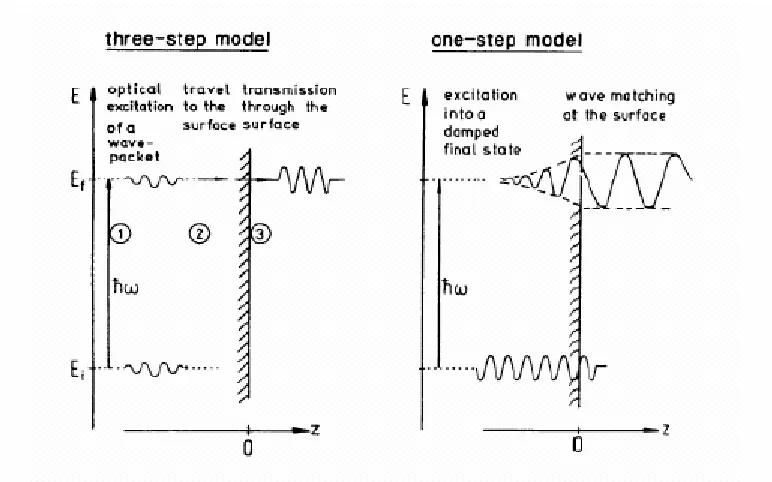
2.3.1.2.4. The three-step and one-step models
There are two main approaches to the theory of photoemission, both of which employ the independent particle approximation. The first, the three-step model, assumes direct transitions between states of the crystal. In a simple approximation the cross-section can
remain unperturbed. This approximation is better known as the “frozen orbital approximation” and the binding energy can be calculated by the Hartree-Fock theory. The binding energy calculated in this way is better known as Koopmans binding energy. The second method, the one step model is based on the scattering theory initially developed for the analysis of low energy electron diffraction beam intensities.
The three-step model
The three-step model was developed by Berglund and Spicer [108]. As the name suggests, the photoemission process is considered to comprise three steps:
(1) In the first step, the photon enters the solid and excites an electron from an initial state of energy Ei to a final state Ef, where Ef lies above the vacuum level. The first step
takes into consideration the interaction between an electron and its initial state and an electromagnetic field. The optical excitation can be determined by the x-ray absorption cross-section (§ 2.3.1.2.2).
(2) The second step involves propagation of the excited electron to the surface, and takes into account inelastic scattering and an effective mean free path for the excited electron [109, 110].
(3) In the final step, the electrons can either be transmitted across the barrier or be reflected back, the escaping electrons being those that have enough energy normal to the surface to overcome the surface barrier.
It was shown [111] that in the limit of sufficiently weak electron damping, the transition matrix elements become the usual crystal-momentum conserving matrix elements. Thus, besides the energy conservation, the crystal momentum is conserved within a reciprocal lattice vector G:
f i
k = +k G (Eq. 2.16)
Umklapp processes (i.e. assisted by a reciprocal lattice vector) as they involve absorption of a photon and diffraction by the crystal lattice through a lattice vector G. The momentum of the photon can be neglected for energies in the VUV and thus, only vertical transitions are allowed. If the final state energy is large enough, and in the absence of inelastic scattering, the electron can be emitted in the vacuum. By passing through the surface, the components parallel to the surface of the final state electron momenta inside and outside the solid are related by
i o
f // f //
k =k +g (Eq. 2.17)
where g is a reciprocal lattice vector of the surface.
The primary photoelectron distribution (for a given symmetry direction in the Brillouin zone) may be written as:
(
) (
)
( )
N hω,E =P hω,E D( )TE E (Eq. 2.18)
where P
(
hω,E)
is the photoionisation probability, D(E) is the probability of an electronescaping without being scattered and T(E) is the probability of an electron being transmitted across the surface barrier. This model is an approximation since these terms are not truly independent. Berglund and Spicer [108] found that the description of the transport can be described in terms of the electron mean free path λe and the optical
attenuation length of the incident photons λph at energy ħω, and D(E) is given by:
( )
e( )
( )
ph( )
( )
e ph
/ D E
1 /
λ λ
=
+ λ λ
ω
ω
E E
h
h (Eq. 2.19)
For electrons of energy E>EF +Φ excited into plane-wave like final states where 2 2
/ 2
=
E h k m, an escape cone of angle θ relative to the surface normal is defined:
cosθ= Φ+EF
If the distribution of electrons within the solid is isotropic then the escaping fraction is given by:
(
)
1
T( ) 1 cos
2 0
;
;
= − +
= +
F
F
E θ E > E Φ
E < E Φ
(Eq. 2.21)
In general, D(E) and T(E) may be expected to distort the energy distribution of emitted electrons. However they slowly vary with energy; thus sharp structure in N
(
hω,E)
must result from P
(
hω,E)
. P(
hω,E)
is given through momentum conservingtransitions from occupied states Ei into unoccupied states Ef. Thus over all possible final states:
( )
( )
( )
2 3
f i f
i,f
P(hω, )E ∝
∑∫
d k f p i δEf k −Ei k −hω δ Ef k −E (Eq. 2.22)For a constant dipole matrix element Mfi = f p i the so-called energy distribution of the joint density of states is obtained:
( )
( )
( )
3
f i f
i,f
P(hω, )E ∝
∑∫
d k⋅δEf k −Ei k −hω δ Ef k −E (Eq. 2.23)and the photoelectron distribution curve is a distorted version of the initial and final state densities. The three-step model therefore predicts a feature in the energy distribution curve when an occupied state at energy Ei is separated from an unoccupied state at the same k (direct transition). The three-step model is limited, as it cannot accommodate surface effects on either the bulk initial of final state wavefunctions. Other problems with this model associated with the first two steps are also experienced [112]. As a consequence, one-step photoemission models have been developed.
Fig. 2.12. Comparison of the three-step (left) and one-step (right) models in the theoretical treatment of the photoemission process.
The one-step model
2.3.1.2.5. Symmetry of wavefunctions
In many photoemission experiments the electron energy distributions are measured normal to the sample surface. Some interesting selection rules associated with the symmetry of the initial and final state wavefunctions then apply. Hermanson [116] showed that for normal emission, or emission in a plane containing the surface normal, the one-electron final state is invariant under crystal symmetry operations that leave the surface component of the measured momentum unchanged. Hermanson pointed out that the parity of the final state wavefunction must be even with respect to the mirror plane for there to be measurable current at the detector. So only an initial state with the symmetry of the dipole operator itself gives rise to dipole allowed transitions. Thus for
⊥
A , A p has odd parity so that optical transitions from odd initial states only are ⋅
allowed. For A the converse is true, // A p is even and transitions from even initial ⋅
states only are allowed. This selection rule is useful for identifying both bulk and surface states in ARUPS data.
2.3.1.3. Concentric hemispherical analysers (CHA)
In order to record a photoemission spectrum, the photoelectrons have to be separated according to their kinetic energy. In all experiments in this work a concentric
Fig. 2.13. Diagram of concentric hemispherical analyser (CHA). Electrons pass between the two
concentric spheres (Rin and Rout) and are collected at the exit slit.
Deflected electrons follows a path of radius Ro where,
2
+ = in out 0
R R
R (Eq. 2.24)
Rin is the radius of the inner hemisphere and Rout is that of the outer hemisphere. The potential of the outer hemisphere (Vout) must be,
3 2
= −
0
out 0
out
R V E
R (Eq. 2.25)
and the potential of the inner hemisphere must be,
3 2
= −
0
in 0
in
R V E
[image:41.595.171.420.63.340.2]The absolute resolution of an analyser ∆E is usually defined as the full-width at
half-maximum of a given peak. The resolving power of an analyser is usually expressed as
∆ 0
E E.
If the voltages on the spheres are varied and hence the pass energy Eo, then the relative resolution of the analyser will vary with Eo across the spectrum. For this reason the electrons are usually retarded before they enter the analyser and the pass energy is kept constant. This enables to keep the absolute resolution constant over a spectrum.
The most common type of electron detector used in such analysers is a channeltron. The channeltron consists of a small glass spiral coated on the inside with a resistive material and across which a voltage has been applied. When an electron reaches the channeltron it will strike the inner wall of the tube and cause secondary emission of electrons. Due to the applied voltage these electrons will be accelerated along the tube causing further secondary emission. The result is an avalanche effect; a single electron may result in an output pulse of ~108 electrons. These pulses are then counted electronically.
For an analyser such as has been described above the relative resolution is usually expressed as,
2
∆ = + α
0 0
E s
E R (Eq. 2.27)
2.3.1.4. Core level shift spectroscopy
Each element has its own ‘fingerprint’ core level spectrum so it is possible to do element analysis. Moreover, the binding energy is sensitive to the chemical environment of the element, providing chemical analysis. In addition, atoms at the surface of the sample may have a different environment compared with the bulk due to missing nearest neighbours and surface reconstruction. Thus they may experience a change in bonding geometry and in chargedistribution. Therefore, the core level binding energies of surface atoms are generally expected to shift with respect to the bulk value. Surface core level shifts (SCLS) provide important information concerning the electronic and atomic structure and it becomes possible to distinguish the environment of the same element (e.g. bulk, surface, dimers, interface). Such shifts are also experienced when an adlayer is deposited due to the chemical or physical interaction of the adlayer with the substrate. Although photoemission is not properly a structural technique, a correct assignment of the SCLS of the inequivalent surface atoms can provide useful information about the surface structure.
To do such an analysis one needs to fit the raw data and to assign components to each supposed “chemical” environment of the element. The overall core level peak lineshape is a convolution of a gaussian and lorentzian profile, also called a Voigt profile [117]:
4
4
I( ) G( ) L( )d + σ
− σ
=
∫
×G
E E E E (Eq. 2.28)
with the gaussian component:
2
G
( )
G( ) exp 4 ln(2)
−
= −
Γ
G
E E
E (Eq. 2.29)
2
L 1 L( )
1 4
=
−
+
Γ
L E
E E
(Eq. 2.30)
where EG (EL) is the centroid of the gaussian (lorentzian) and ΓG (ΓL) is the FWHM.
The lorentzian broadening is associated with the finite lifetime of the core hole. The gaussian broadening is due to surface inhomogeneity, phonon broadening, thermal broadening and the non-zero resolution of the monochromator and detector. The gaussian width can vary when an interface is modified due to a different chemical environment which can modify the phonon spectrum. In the case of a metal an extra parameter accounting for an asymmetry of the peak needs to be added. In that case the lorentzian function is replaced by the Doniach and Sunjic function. This can also be required at semiconductor surfaces when the substrate surface atoms form metallic droplets.
Levels with a non-zero value of the orbital angular momentum quantum number (l > 0), i.e. p, d, f… levels, show spin-orbit-splitting. This is due to the electromagnetic
coupling of the orbital momentum l and the spin momentum s which results in the total angular momentum j where:
j=l+s and s = ±1/2 (Eq. 2.31)
The number of states for each total angular momentum is given by 2j+1, the degeneracy and is therefore different for each value of j. This results in two peaks of different energy and intensity. The intensity ratio between the two peak components is called the branching ratio R and is generally described by [118]:
2
1
I 2( ) 1
I 2( ) 1
− + =
+ +
l s
l s = R (Eq. 2.32)
2.3.1.5. Growth mode
Incident X-rays penetrate several microns into the sample. However electrons travel much smaller distances in solids. They lose energy through inelastic scattering events that can be due to hole pair excitation, plasmon excitation, electron-phonon scattering or electron-impurity scattering. These events produce a secondary electron background upon which the main features are superimposed. The number of primary photoelectrons that leave the crystal depends exponentially on the distance travelled. The intensity decay can be expressed as:
0
I( ) I exp
( , )
= −
kin
x x
λ E Z (Eq. 2.33a)
where I0 is the original photoelectron intensity, I(x) the intensity remaining after passing
through the distance x within the sample and λ the inelastic mean free path. λ is dependent on the material and kinetic energy. Applying this to the effect of an overlayer
of thickness d, the expression must include, θ, the angle of emission with respect to the surface normal:
0 I( ) I exp
( , ) cos
= −
θ
kin
d x
λ E Z (Eq. 2.33b)
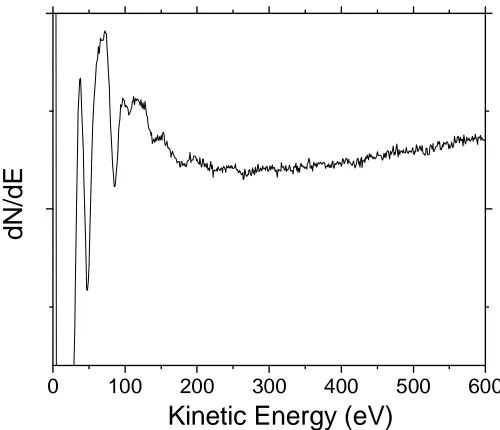
The dependence of λ on the energy follows the so-called “universal curve” which reaches a minimum of about 4 Å around 50 eV kinetic energy (figure 2.14). This is the basis for the surface sensitivity of PES.
From the decay of the substrate core level intensity one can also define the growth mode of the adlayer. For normal emission, the cosine term in equation 2.33b equals unity and the equation can be rewritten:
0 I( ) ln I = − x d
Fig 2.14. Experimental dependence of the mean free path versus electron kinetic energy [119]
There is a linear dependence between 0 I( ) ln
I
x
and the thickness of the adlayer. By
plotting the expected model for a uniform film growth and comparing it to the experimental substrate intensity decay, three main growth modes can be distinguished
(figure 2.15).
Firstly, with layer-by-layer growth (or Frank-van der Merwe growth), the arriving molecules form first a complete monolayer, followed by the growth of further complete monolayers. This case corresponds to a uniform film growth and as described above
there is a linear dependence between 0 I( ) ln
I
x
and the thickness of the adlayer with a
slope equal to −1
λ . Secondly, with island growth (or Volmer-Weber growth) small
than −1
λ . Such growth results when the interaction between the molecules of the
overlayer is stronger than the interaction of the molecules with the substrate. Finally, with layer plus island growth (or Stranski-Krastanov growth), a few complete monolayers grow during the initial stage of the growth, subsequently followed by the nucleation of islands on top of these monolayers. For such a growth, the intensity decay exhibits two distinct behaviours, uniform film growth for the first few complete
monolayers and linear with a slope larger than −1
λ for the rest of the film.
substrate
ln I/Io
thickness (Å)
(1) layer-by-layer (Frank - van der Merwe)
substrate
ln I/Io
thickness (Å)
(2) islands (Volmer - Weber)
substrate
ln I/Io
thickness (Å)
(3) layer(s) + islands (Stranski - Krastanov)
substrate
ln I/Io
thickness (Å)
(1) layer-by-layer (Frank - van der Merwe)
substrate
ln I/Io
thickness (Å)
(1) layer-by-layer (Frank - van der Merwe)
substrate
ln I/Io
thickness (Å)
(2) islands (Volmer - Weber)
substrate
ln I/Io
thickness (Å)
(2) islands (Volmer - Weber)
substrate
ln I/Io
thickness (Å)
(3) layer(s) + islands (Stranski - Krastanov)
substrate
ln I/Io
thickness (Å)
(3) layer(s) + islands (Stranski - Krastanov)
Fig. 2.15. Representation of three different types of growth mode, Frank – van der Merwe, Volmer – Weber and Stranski – Krastanov (top). Expected decay profile of the substrate core level for each type of growth (bottom).
2.3.1.6. Energetics
organic adlayer and the ionisation energy (IE) of both the clean substrate and the organic film.
E
FVBM
HOMO-edge
Vacuumlevel
Vacuum level D
Substrate
Organic film
IE
sIE
adlayerE
FVBM
HOMO-edge
Vacuumlevel
Vacuum level D
Substrate
Organic film
IE
sIE
adlayerFig. 2.16. Energy band alignment of a substrate/organic film interface. VBM represents the valence band
maximum, HOMO-edge is the edge of the highest occupied molecular orbital level, EF the Fermi level, IE
the ionisation energy and ∆ the interface dipole.
1 0 -1
2 1 0 -1
60Å SnPc
I
n
te
n
s
ti
y
(
a
.u
.)
Binding Energy (eV) Clean surface
The VBM is determined by the extrapolation of the valence band emission (figure 2.17, left). The equivalent to the valence band maximum for the organic film is the HOMO-edge (highest occupied molecular orbital) and is determined in the same way (figure 2.17, right).
The ionisation energy of the substrate (or adlayer) is the difference between the photon energy and the width of the energy distribution curve (EDC). In practice, measuring the EDC width is achieved by biasing the sample to ensure the collection of the low energy secondary electron cut-off.
EDC width H O M O -e d g e D e n s it y o f s ta te s 0 C u t o ff , E v a c Core levels Valence Band Kinetic energy
Fig. 2.18. Diagram representing the energy distribution curve width
From these values it is possible to establish the valance band offset, the interface dipole and the position of the conduction band. The valence band offset is defined as the difference between the VBM of the substrate and the HOMO-edge the organic film at
the interface. Thus it is necessary to know the position of the valence band maximum at
the interface. This is assumed to be the value at the clean surface plus the amount by which the band bending is reduced in the final coverage. The change in band bending can be measured through the energy shift of the substrate core level.
To obtain the interface dipole between the two materials at their interface, the respective vacuum levels need to be determined. This is done by aligning the Fermi level on each
the HOMO-edge positions and the respective ionisation energies. The interface dipole is then the difference between the vacuum levels of the substrate and the organic film.
The conduction band is easily obtained for the inorganic substrate by adding the bandgap to valence band value. It is more complicated for the inorganic film. The energy difference between the highest occupied molecular orbital (HOMO) and the lowest unoccupied molecular orbital (LUMO) (i.e. the HOMO-LUMO bandgap) may be considered as being analogous to the energy bandgap in inorganic semiconductors. For inorganic semiconductors, band-gap measurements are often made using photoluminescence techniques which give a value for the optical band-gap (Eopt) which
is considered to be a good value for the transport band-gap (Et), defined as the minimum
energy required to create a free electron and hole. This is acceptable in the case of inorganic semiconductors due to the relative insignificance of effects such as charge carrier screening and polarisation; exciton (electron-hole pair) binding energies can be ignored. This is not the case for organic semiconductors where the exciton binding
energies can be significant and hence the optical gap cannot give an accurate value of the transport gap. Measurements of the HOMO-LUMO band-gap for many organic molecules have been performed by Kahn et al [120] using valence-band UPS measurements and inverse photoemission (IPES) spectra. For example for CuPc, the transport gap is 0.6 eV larger than the optical gap.
Using all those assumptions, the energetics at an organic/inorganic semiconductor heterojunction can be established.
2.3.2. Near Edge X-ray Absorption Fine Structure (NEXAFS)
ionisation edge. Near the ionisation edge the electron has a low kinetic energy and, in a molecule, can be excited into unoccupied orbitals below the vacuum level (see figure 2.19) [104]. The resulting fine structure of the X-ray absorption cross section reflects the electronic structure of the unoccupied molecular states.
Fig. 2.19. Schematic effective potentials and the corresponding absorption spectra.
X-rays
E
π* orbital
X-rays
E
π* orbital
π*
π*
σ*
σ*
X-rays
E
π* orbital
X-rays
E
π* orbital
π*
π*
σ*
σ*
Fig. 2.20. Representation of the link between the orientation of the molecule, the polarised light and the expected spectra.
linearly polarised X-ray beam with respect to the corresponding transition dipole. For
π*-states, for example, the photoabsorption cross-section has a specific dependence on the orientation of the molecule relative to the polarisation of the radiation. For
phthalocyanine, the delocalised π system is perpendicular to the plane of the molecule. So if the molecule lies flat, as in the example of figure 2.20, the characteristic peak of
π* features grows with increasing angle of incidence. The π* and σ* absorption have opposite angle-dependences.
The intensity of the π* features is proportional to the square cosine of the angle between the polarisation vector E and the πorbital (Eq. 2.35).
β ∝cos²
I (Eq. 2.35)
x z
y h ν
E
Π
θ
φ β α
x z
y h ν
θ
φ β α
Fig. 2.21. Angle description of NEXAFS scheme. The electron field Eis in the xz plane. Π represents
the π orbital direction for a molecule with a tilt angle α, in a general azimuth φ from x. α, the tilt angle
of the molecule, is the angle between Π and the surface normal. It is also the angle between the plane of
the molecule and the surface of the substrate. θ is the angle of incidence of the photon beam with respect
to the surface normal and β is the angle between E and Π.
![Fig. 2.6. Monoclinic crystalline structure of lead phthalocyanine adapted from [72]](https://thumb-us.123doks.com/thumbv2/123dok_us/8802145.914499/23.595.216.411.70.266/fig-monoclinic-crystalline-structure-lead-phthalocyanine-adapted.webp)
![Fig. 2.9. Adsorption model of PbPc on c(8×2)-InSb(100) reconstruction [92]](https://thumb-us.123doks.com/thumbv2/123dok_us/8802145.914499/27.595.150.479.257.509/fig-adsorption-model-pbpc-c-insb-reconstruction.webp)

![Fig 2.14. Experimental dependence of the mean free path versus electron kinetic energy [119]](https://thumb-us.123doks.com/thumbv2/123dok_us/8802145.914499/46.595.102.529.86.353/fig-experimental-dependence-mean-versus-electron-kinetic-energy.webp)