2019 International Conference on Computer Science, Communications and Multimedia Engineering (CSCME 2019) ISBN: 978-1-60595-650-3
A Combinational Logic Controller Based on Proteus
Da-wei XIAO and Tian-yu HE
City institute, Dalian university of technology, Dalian, 116600, China
Keywords: Proteus, Keil, Combinational logic controller, Computer organization.
Abstract. Proteus and Keil are used to implement a combinational logic controller. Firstly, the instruction system, instruction flow and control signal of the controller are designed. Secondly, the logical expressions of each control signal are listed and simplified. Then, the circuit schematic diagram of the combinational logic controller is drawn by Proteus software. Finally, using Keil, the program is loaded and run in the controller, which is verified by simulation. This design uses logic devices, improves the execution speed of instructions, and enhances the flexibility of design. In the experiment teaching of Computer Organization course, it can improve students' thinking ability and practical ability well.
Introduction
The controller is the command and control center of the computer. According to different design methods, it is divided into combinational logic controller and microprogram controller [1]. The combinational logic controller consists of instruction decoding circuit, sequential circuit and combinational logic circuit. The instruction decoder determines the currently executed instructions, combines the beat generated by the sequential circuit, and jointly acts as the input of the combinational logic circuit, and outputs the corresponding control signal. Combinational logic controllers are composed of complex combinational logic gates and flip-flops, which have fast execution speed. Therefore, they have been widely used in new computer structures such as RISC in recent years [2].
Machine Instruction Design
Instruction Code and Functions
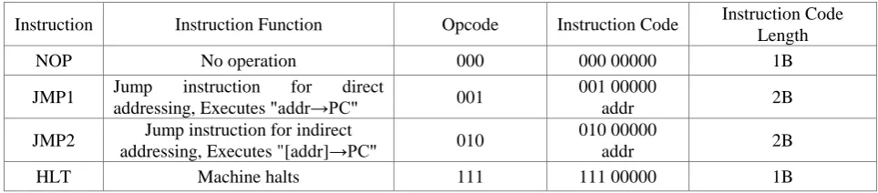
[image:1.595.56.538.574.680.2]This controller can realize direct and indirect addressing, so four instructions of NOP, JMP1, JMP2 and HLT are designed. The instruction code and its functions are shown in Table 1.
Table 1. Machine instruction list.
Instruction Instruction Function Opcode Instruction Code Instruction Code Length
NOP No operation 000 000 00000 1B
JMP1 Jump instruction for direct
addressing, Executes "addr→PC" 001
001 00000
addr 2B
JMP2 Jump instruction for indirect
addressing, Executes "[addr]→PC" 010
010 00000
addr 2B
HLT Machine halts 111 111 00000 1B
jumped address, so the length of instruction code is designed to be 16 bits, the high 8-bits are "00100000" and "01000000" respectively, and the low 8-bits are "addr".
Instruction Flow
During the execution of these four machine instructions, the largest number of States is JMP2 instructions with three states. The controller adopts a single-period structure, by this standard, the state machine of the controller consists of three states: S1, S2 and S3. In each state, the operation of "Source Component→Bus→Target Component" is executed. So, in each state, the two beats are designed, which are recorded as T1 and T2. The operation is "Source Part→Bus" in T1 and the operation is "Bus→Target Component" in T2 [3].
Thus, the state flow chart of the four machine instructions execution process is shown in Figure 1.
T1:PC→AR,ROM→BUS T2:BUS→IR,PC+1→PC
Opcode=?
Machine Halt HLT T1:PC→AR,ROM→BUS
T2:BUS→PC JMP1
~ ~
【S1】
【S2】
T1:PC→AR,ROM→BUS T2:BUS→PC
【S2】
T1:PC→AR,ROM→BUS T2:BUS→PC
T1:
T2:
【S3】 【S3】
T1:
T2:
T1:
T2: 【S2】
【S3】
JMP2 NOP
Fetch Cycle
Execute Cycle
Figure 1. Instruction Flow Figure.
Micro-command Design
As shown in Figure 1, the following micro-commands are required to execute four instructions: NOP, JMP1, JMP2 and HLT (Bus has no input and output control signals):
PC→AR: This operation requires two micro-commands, one is PC output, recorded as PCOUT and the other is AR loading, recorded as LDAR.
ROM→BUS: This operation requires a micro-command, which is ROM output, and the ROM output control signal is usually low level effective, so the ROM output is recorded as /OE.
BUS→IR: This operation requires a micro-command, which is IR loading, recorded as LDIR. PC+1→PC: This operation requires a micro-command, which is PC plus 1, recorded as PC_INC. BUS→PC: This operation requires a micro-command, which is PC loading. The signal is also low level effective, so it recorded as /LDPC.
As can be seen from Figure 1, the micro-command signal is the result of "and" or “OR” operation between the current machine instruction signal and the specific beat signal. In all the following expression, “*” is AND operation, “+” is OR operation ).
[image:2.595.88.512.240.399.2]Table 2 shows the states associated with each micro-command signal.
Table 2. Micro-command related state list.
Micro-command Related State
NOP/HLT JMP1 JMP2
LDAR S1 S1、S2 S1、S2、S3
/OE S1 S1、S2 S1、S2、S3
LDIR S1 S1 S1
PC_INC S1 S1、S2 S1、S2、S3
The logical expressions of these micro-command refer with Eq. 1~3.
LDAR=/OE=PC_INC=S1+(JMP1+JMP2)*S2+JMP2*S3. (1)
LDIR=S1. (2)
/LDPC=(JMP1+JMP2)*S2+JMP2*S3. (3)
Combinational Logic Controller Circuit Design
The circuit of the controller consists of data path, instruction decoding circuit, sequential circuit and combinational logic circuit.
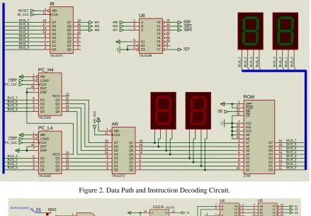
Data Path and Instruction Decoding Circuit
This part of the circuit consists of program counter PC, address register AR, program memory ROM, instruction register IR and instruction decoder.
Both AR and IR are composed of latch 74LS273. AR is used to store the address of the access program memory. IR is used to store information such as instruction codes or addresses read from program memory.
ROM is composed of 2764 chips for storing machine language programs. There are two green tubes on the left to display instruction codes or addresses read from memory, and two red tubes on the right to display addresses currently accessing memory.
PC is composed of 74LS163 which is a 4-bit binary synchronous counter. ENP, ENT, MR, CLK, LOAD, D3-D0 are the input and Q3~Q0 are the output.
Since LDIR, PC_INC and LDAR are CLK signals and CLK signals are edge signals, so the three signals must be combined with the beat signal T1 or T2 of the specified period to produce new edge trigger signals, which are recorded as IR_CLK, PC_CLK and AR_CLK. The logical expressions of these CLK signals refer with Eq. 4~6.
IR_CLK=LDIR*T2. (4)
PC_CLK=PC_INC*T2. (5)
AR_CLK=LDAR*T1. (6) Instruction decoder is composed of 74LS138 which receives opcodes (IR7-IR5) of instructions and generates valid signals corresponding to four instructions after decoding.
Data Path and Instruction Decoding Circuit are shown in Figure 2.
Sequential Circuit
The sequential circuit consists of reset switch, clock signal source and beat sequence.
The reset switch is realized by a dial switch. When dialed to a high level state, the ON signal can be validated by 74LS74 trigger. S, R, CLK and D are the inputs of 74LS74 and Q and/Q are the outputs of 74LS74.
There are two kinds of clock signal sources: automatic signal source AUTO_CLK and manual signal source MANUAL_CLK. The automatic signal source can output a continuous clock signal, while the manual signal source only outputs a clock signal at each switch press. In order to observe the results of each step of the application, the manual signal source is used to realize the one-step operation of the application.
In the beat sequence, T1 and T2 beats are generated by a 74LS74 flip-flop, and the state signals S1~S3 are generated by 74LS74 flip-flop, 74LS139 decoder and 74LS240 reverse output driver.
The sequence circuit diagram is shown in Figure 3.
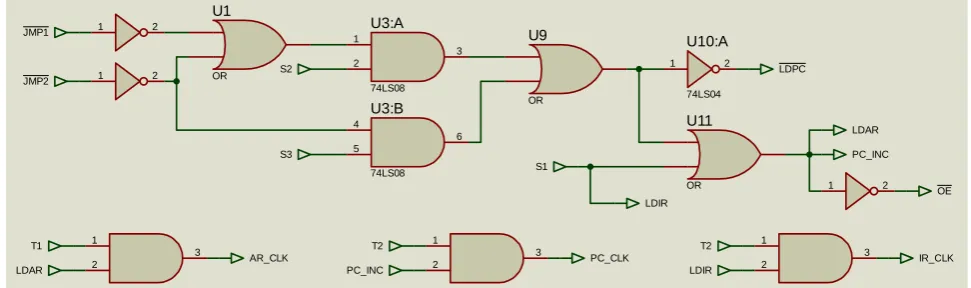
Combinational Logic Circuit
In this part of the circuit, NOP, JMP1, JMP2 and HLT command signals are generated by 74LS138 decoder, which are all low level effective signals. Then, the simulation circuit diagram is drawn according to the micro-command logic expression (refer with: Eq. 1~6).
The combined logic circuit is shown in Figure 4.
BUS_0 BUS_1 BUS_2 BUS_3 BUS_4 BUS_5 BUS_6 BUS_7 B U S _ 7 B U S _ 6 B U S _ 5 B U S _ 4 B U S _ 3 B U S _ 1 B U S _ 2 B U S _ 0 BUS_7 BUS_6 BUS_5 BUS_4 BUS_3 BUS_2 BUS_1 BUS_0 BUS_7 BUS_6 BUS_5 BUS_4 BUS_3 BUS_2 BUS_1 BUS_0 A0 10 A1 9 A2 8 A3 7 A4 6 A5 5 A6 4 A7 3 A8 25 A9 24 A10 21 A11 23 A12 2 CE 20 OE 22 PGM 27 VPP 1 D0 11 D1 12 D2 13 D3 15 D4 16 D5 17 D6 18 D7 19 ROM 2764 OE A R _ C L K A 1 B 2 C 3 E1 6 E2 4 E3 5 Y0 15 Y1 14 Y2 13 Y3 12 Y4 11 Y5 10 Y6 9 Y7 7 U8 74LS138 HLT JMP2 JMP1 NOP IR7 IR6 IR5 D0 3 D1 4 D2 7 D3 8 D4 13 D5 14 D6 17 D7 18 CLK 11 MR 1 Q0 2 Q1 5 Q2 6 Q3 9 Q4 12 Q5 15 Q6 16 Q7 19 AR 74LS273 D0 3 Q0 14 D1
[image:4.595.79.519.217.522.2]4 D2 Q1 13 5 Q2 12 D3 6 Q3 11 RCO 15 ENP 7 ENT 10 CLK 2 LOAD 9 MR 1 PC_L4 74LS163 D0 3 Q0 14 D1 4 Q1 13 D2 5 Q2 12 D3 6 Q3 11 RCO 15 ENP 7 ENT 10 CLK 2 LOAD 9 MR 1 PC_H4 74LS163 LDPC PC_CLK LDPC PC_CLK D0 3 D1 4 D2 7 D3 8 D4 13 D5 14 D6 17 D7 18 CLK 11 MR 1 Q0 2 Q1 5 Q2 6 Q3 9 Q4 12 Q5 15 Q6 16 Q7 19 IR 74LS273 RESET IR_CLK IR7 IR6 IR5
Figure 2. Data Path and Instruction Decoding Circuit.
D 2 Q 5
CLK 3 Q 6 S 4 R 1 ON RESET D 2 Q 5
CLK 3 Q 6 S 4 R 1 U6 74LS74 T1 D 2 Q 5
CLK 3 Q 6 S 4 R 1 U7 74LS74 T1 RESET SW1 SW -SPDT RESET MANU_CLK R1 1k 1 2 13 12 CLK SW2 SW -SPDT A 2 Y0 4
B 3 Y1 5
Y2 6 E 1 Y3 7 U4 74LS139 A0 2 A1 4 A2 6 A3 8 OE 1 Y0 18 Y1 16 Y2 14 Y3 12 U5 74LS240 S1 S2 S3 MANU_CLK ON HLT AUTO-CLK(NC) J 14 Q 12
CLK 1
K 3 Q 13
[image:4.595.92.509.495.635.2]R 2 U12:A74LS73 T2 T1 RESET CLK
1 2
3 T2
LDIR
IR_CLK 1
2
3 T1
LDAR
AR_CLK
1 2
3 T2
PC_INC
PC_CLK JMP1
JMP2
1 2
S2
1 2
S3
LDPC
S1
PC_INC LDAR
1 2 OE
LDIR
U1
OR
1 2
3
U3:A
74LS08
4 5
6
U3:B
74LS08
U9
OR
1 2
U10:A
74LS04
U11
[image:5.595.54.540.73.217.2]OR
Figure 4. Combinational Logic Circuit.
Simulation and Verification
Application Design
The machine instruction code is 8 bits, each piece 2764 is also 8 bits, so the ROM is composed of one piece 2764. Keil software is used to store the following code in ROM:
ORG 0000H
DB 20H ; JMP1 03H DB 03H
DB 00H ; NOP DB 40H ; JMP2 07H DB 07H
DB 0E0H ; HLT DB 00H ; NOP DB 05H ; Addr END
Start Simulation
Put the CLK switch to the MANUAL_CLK position. First set RESET=0, then RESET=1, therefore the CLK starts to output and enters the S1 state and T1 beat.
In T1 beat of S1 state, effective micro-commands are /OE and LDIR. Therefore, ROM outputs 20H stored in 00H address unit. At this time, red digital tube displays 00H and green digital tube displays 20H, which is the first instruction of the application. At the moment, IR_CLK is still invalid, so even if the green digital tube in the data path displays 20H, it means that the opcode part of the "JMP1 03H" instruction has been taken out, in fact, the op-code has not been written to IR.
Run Application
Table 3. Instruction running sequence record table. Sequence
Number
Red Digital Tube (Display Address)
Green Digital Tube (Display Instruction Code)
Currently Executed Instructions
1 00H 20H
JMP1 03H
2 01H 03H
3 03H 40H
JMP2 07H
4 04H 07H
5 07H 05H
6 05H E0H HLT
Summary
This paper completes the design of a combinational logic controller, which realizes the functions of direct and indirect addressing. The controller is designed by Proteus, which makes the controller easy to modify, enhances the design flexibility and improves the execution speed of instructions. In the future, more executable instructions will be added to strengthen the function of the controller.
References
[1] Liqiu Jiang, Dawei Xiao, Computer Composition and Design, Dalian University Of Technology, Da Lian, 2009.
[2] Yan Gao, Kun Fu, Shuzhen Luo, etc., Combinational Logic Controller in the Model Machine Based on FPGA, Laboratory Research and Exploration. 34 (2015) 86-91.