© 2015, IRJET ISO 9001:2008 Certified Journal
Page 1321
WAFER STAGE MOTION CONTROL
Nithin Krishnan J.R
11
PG Student, Control Systems, Dept. of EEE, LMCST, Kuttichal, Trivandrum, India
---***---ABSTRACT
: Wafer manufacturing Industries uses conventional controller, but in order to control the position in sub nanometer range conventional controller is not suitable, why because Tuning and augmenting the controller becomes difficult and expensive. So a robust controller is designed for wafer manufacturing system. The controller design in this paper is performed for the translational x and y DOFs in the horizontal plane to facilitate the exposition. The trends in wafer stages are expected to lead to lightweight precision motion systems. In order to make the wafer manufacturing system more efficient and to increase its accuracy, here in this paper a comparison between H infinity and Fuzzy PI controller is designed and compare their result.KEYWORDS: Wafer Manufacturing Systems, Fuzzy PI
Controller, H infinity Controller.
1.
INTRODUCTION
Semiconductor industry serves an extraordinary
revolution in both materials science and in data processing and storage. As recently as 1980, most individuals had no idea that computers would ever impact their personal lives. Today, many families own one or two computers, and use many other computers and dedicated processor systems in their appliances and automobiles. As the increasing demands in electronics filed we must require such an accurate and speedy
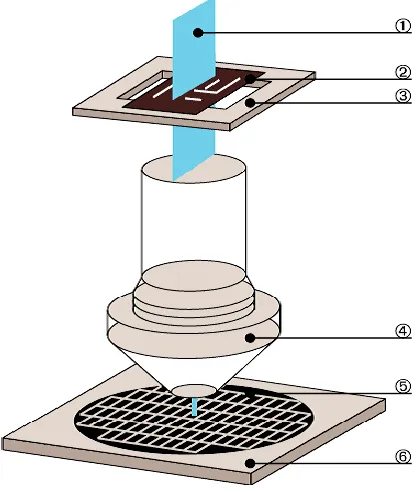
Schematic illustration of a wafer scanner system is shown in Fig 1. In which1 represents light source,2 represents reticle,3 represents reticle stage,4 represents lens,5 represents wafer and 6 represents the wafer stage, see [7]. The light source coupled with the condenser lens comprises the illumination system. The lens element is a combination of several refractive (glass) and reflective (mirror) pieces. The purpose of the illumination system is to deliver light from the source onto the mask, with specified intensity, directionality, and uniformity see
[3]-[4]. The light passes through the transparent portions of the reticle where it is diffracted by the glass. The light then passes through the objective lens, which projects the image onto the wafer surface. The resist in the exposed areas of the wafer surface is soluble in a particular solvent and thus can be removed. When the wafer is developed, the pattern on the reticle is transferred to the wafer surface and is now ready for the next operation. The smaller the geometries, the narrower the margin of error, thus requiring stringent control capabilities, see [1].
2.WAFER STAGE CONTROL FRAMEWORK
Industrial wafer stage systemconsists of a moving coil permanent magnet planar motor is especially designed for vacuum operation. The system consists of plate consisting of an ordered array of permanent magnets and a mover which consists the moving part of the wafer stage, see [9].Inorder to produce necessary force four actuators are connected to the mover, each consisting of three coils, which are powered by a three-phase power source. By means of an appropriate position-dependent commutation of the coils, each actuator delivers a well-defined and reproducible force in two directions, see [8].
During wafer manufacturing process first the wafer is covered by a thin insulating layer and with a light sensitive material called photoresist.Thesystem projects postage- stamp-size patterns onto the wafer until the entire wafer is covered with identical microchip patterns. The exposed areas of the photoresist are weakened when the light hits them, and then a corrosive plasma etches the pattern into the silicon. The leftover photoresist is washed away, leaving the photoresist pattern engraved into the semiconductor wafer. The process has gotten more complicated with each generation of shrinking features. Lithography toolmakers have had to reduce the wavelengths of light they use to project chip patterns through the masks. They’ve also had to find heroic optical tricks to finesse the light into depositing patterns far smaller than the wavelengths themselves
© 2015, IRJET ISO 9001:2008 Certified Journal
Page 1322
(1)
(2)
(3)
(4)
(5)
(6)
(7) (8)
(9)
Fig -1: Schematic diagram of a Wafer System
3. CONTROLLER DESIGN
Industrial wafer manufacturing system have six DOFs i.e., three translational and three rotational DOFs. Here I am going to design two controllers for two DOFs i.e. in x and y directions. Block diagram for the wafer manufacturing system is shown in fig 2. The input u, control output y to the system, plant and the two reference signal is taken as,
Fig-2: Feedback configuration for wafer stage
3.1 H Controller Design
For a feedback H controller the infinity norm of the cost
function should be minimum as possible cost function of the system is given by (6), W and V are the weighting filters.
Cost Function of the system is given by (9), our aim is to find such a controller to reduce the value of cost function.
[image:2.612.328.558.86.271.2] [image:2.612.38.247.132.378.2]© 2015, IRJET ISO 9001:2008 Certified Journal
Page 1323
(10)
(11)
(12)
Where Ws and Wt are the weight functions assigned to the problem by the designer. The ultimate aim of the robust control is to reduce the effect of disturbance on output. So sensitivity S and the complementary function T are to be
reduced. Considered model-based control design
procedure is to compute the controller Copt that minimizes J (P, C)) in (6) for the true system Po,i.e., Copt
=argminCJ (P0, C)) Po represents the unknown physical
wafer stage system (augment plant model),the weighting filters W and V are designed using a loop-shaping technology based design procedure. For H design two transfer function method is used here.
3.2 Fuzzy PI Controller Design
To control the wafer manufacturing system in sub nanometer range H∞ controller requires too much of iteration process so it requires huge amount of time to control the plant that’s why here Fuzzy PI controller is designed[10]-[12].Generalized Fuzzy PI control output is given by (12).
Where ∆kp and ∆ki are the variations in proportionality and integral gain of the fuzzy PI controller. For design purpose in order to make output fall in sub nanometer range values of Kp=0.5Gu.Gr & Ki = 0.5Gu.Ge where Gu, Ge, Gr and the scaling factors.Here there are eight Linguistic variables are selected they are Negative Big (NB), Negative Medium (NM), Negative Small (NS), Negative Zero (NZ), Positive Zero (PZ),Positive Small (PS),Positive Medium (PM),Positive Big(PB).Fuzzy rule base is given below. After getting the μ values for ∆Kp and ∆Ki deffuzification process starts here Centre of gravity method is used.
Fig-3: Fuzzy output (i) error and change in error, (ii) ∆Kp and ∆Ki
Fig-4: Control surface for Fuzzy PI controller
Table-1: Step response Parameters of controllers
H infinity
controller
Fuzzy PI
controller
Rise time 0.2197 0.0322
Settling time 0.3913 0.0517
Overshoot 0 0.5448
Peak 200 201.0670
© 2015, IRJET ISO 9001:2008 Certified Journal
Page 1324
Fig-5: Step response of the existing and proposed system and results
Fig-6: Error chart for H∞ and Fuzzy PI controller
3.4 CONCLUSIONS
Here next-generation wafer motion control was presented and implemented. The framework was tailored toward next generation motion systems that are expected to be increasingly complex in the sense of high order flexible dynamics and an increasing number of inputs and outputs. Most of the wafer manufacturing industries are now using conventional type of controllers by in order to control it in sub nanometer range these controllers fails, so that’s why two controllers are designed for the wafer manufacturing system and compare the two controllers. From the results it shows that fuzzy PI controller is easy to design and implementing, and it shows sudden reflexes to the sudden changes occurs in the system.
REFERENCES
[1] V. M. Martinez and T. F. Edgar, “Control of
lithography in semiconductor manufacturing,” IEEE Control System, volume 26, no. 6, pp. 46–55, Dec. 2006.
[2] M. van de Wal, G. van Baars, F. Sperling, and O. Bosgra, “Multivariable H∞/μ feedback control design for high-precision wafer stage motion,” Control Engineering Practical vol. 10, no. 7, pp. 739–755, 2002.
[3] D. S. Bayard and R. Y. Chiang, “Identification,
uncertainty characterization and robust control synthesis applied to large flexible structures control,” Int. J. Robust Nonlinear Control, volume 8, no. 2, pp. 97–112, 1998.
[4] U. Schönhoff and R. Nordmann, “A H∞-weighting
scheme for PID-like motion control,” in Proc. Int. Conf. Control Application Glasgow, Scotland, Dec. 2002, pp. 192–197.
[5] R. S. Smith and J. C. Doyle, “Model validation: A
connection between robust control and
identification,” IEEE Trans. Autom. Control, vol. 37, no. 7, pp. 942–952, Jul. 1992.
© 2015, IRJET ISO 9001:2008 Certified Journal
Page 1325
[7] T. Oomen, O. Bosgra, and M. van de Wal,
“Identification for robust inferential control,” in Proc. IEEE Conf. Decision Control, Shanghai, China, Dec. 2009, pp. 2581–2586.
[8] T. Oomen, “System identification for robust and
inferential control with applications to ILC and precision motion systems,” Ph.D. dissertation, Eindhoven Univ. of Technol., Eindhoven, The Netherlands, 2010.
[9] S. Adee, “EUV’s underdog light source will have its
day,” IEEE Spectrum, vol. 47, no. 11, pp. 13–14, Nov. 2010.
[10] J. Espinosa and J. Vandewalle, October 2000,
“Constructing fuzzy models with linguistic integrity from numerical data- AFRELI algorithm”. IEEE Transactions on Fuzzy Systems, 8(5):591– 600.
[11] W. Duch, R. Adamczak, and K. Grabczewski, March
2001,” A new methodology of extraction, optimization and application of crisp and fuzzy logical rules”. IEEE Transactions on Neural Networks, 12(2):277–306.
[12] D. Chakraborty and N.R. Pal, June 2001,”