© 2016, IRJET | Impact Factor value: 4.45 | ISO 9001:2008 Certified Journal
| Page 2942
Optimization of energy consumption in a NOC link by using novel data
encoding technique
Asha J.
1, Rohith P.
21
M.Tech, VLSI design and embedded system, RIT, Hassan, Karnataka, India
2Assistent professor, Dept. Of E&C, RIT, Hassan, Karnataka, India
---***---Abstract -
With advancements in VLSI processtechnology as the number of integration increases in SoC, this leads to increase in the density of on chip wires. Because of this, the performance of the circuit degrades. So network on chip came into existence, NoC is the best solution for scalability issues, but it has its own limitations i.e. the power dissipated by the links of a network-on-chip and also at the other element of communication system, for example the routers and the network interfaces. In this proposed paper, set of data encoding techniques with different schemes will be designed to decrease the power dissipation at network links of NoC, which optimizes the on-chip communication system not only in terms of performance but also in terms of power. These schemes are universal and transparent to construct the NoC fabric that means this application will not require any change in the router and link of architecture.
Key Words: coupling switching activity, data encoding,
interconnection on chip, low power, network-on-chip (NoC), and power analysis.
1. INTRODUCTION
As VLSI technologies continue to scale, wire densities increases to support ever-small transistor geometries and causes on-chip wires to present increasing latency and energy problem. The high latency of cross-chip communication can still limit total performance by increasing the delay between on-chip units. Such scalable bandwidth requirement can be satisfied by using on-chip packet-switched micro-network of interconnects, generally known as Network-on-Chip (NoC) architecture. The basic idea came from the traditional large-scale multi-processors and distributed computing networks. The scalable and modular nature of NOC and their support for efficient on chip communication lead to the NOC based system implementation.
In this paper, focus on techniques aimed at reducing the power dissipated by the network links. In fact, the power dissipated by the network links is as relevant as that dissipated by routers and network interfaces (NIs) and their contribution is expected to increase as technology scales. In particular, we present a set of data encoding schemes operating at flit level and on an end-to-end basis, which allows us to minimize both the switching activity and the coupling switching activity on links of the routing paths traversed by the packets.
2. ENCODING SCHEMES
In the paper, encoding scheme will be implemented whose goal is to reduce power dissipation by minimizing the coupling transition activities on the links of the interconnection network. Let us first describe the power model that contains different components of power dissipation of a link. The dynamic power dissipated by the interconnects and drivers is
[image:1.595.327.547.521.613.2]P = [T0→1 (Cs+Cl) +Tc Cc] V2DD FCK (1)
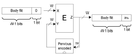
Fig 1: Encoding block diagram.
© 2016, IRJET | Impact Factor value: 4.45 | ISO 9001:2008 Certified Journal
| Page 2943
schemes proposed in this paper and only the block E is [image:2.595.42.282.213.339.2]different for the schemes. To make the decision, the previously encoded flit is compared with the current flit being transmitted.
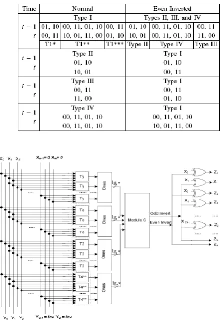
Table I: EFFECT OF ODD INVERSION ON CHANGE OF TRANSITION TYPES
Table above shows the effect of odd inversion on change of transition type. Coupling transition can be classified into four types, A Type I transition occurs when one of the lines switches when the other remains unchanged. In a Type II transition, one line switches from low to high while the other makes transition from high to low. A Type III transition corresponds to the case where both lines switch simultaneously. Finally, in a Type IV transition both lines do not change.
Scheme I
In scheme I, we focus on reducing the numbers of Type I transitions and Type II. The scheme compares the current data with the previous one to decide whether odd inversion or no inversion of the current data can lead to the link power reduction.
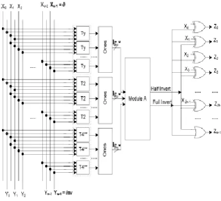
Fig 2: Encoder internal architecture of scheme I.
In the encoding logic, each Tyblock takes the two adjacent bits of the input flits (e.g., X1X2Y1Y2, X2X3Y2Y3, X3X4Y3Y4, etc.) and sets its output to “1” if any of the transition types of Ty is detected. This means that the odd inverting for this
pair of bits leads to the reduction of the link power dissipation (Table I). The Ty block may be implemented using a simple circuit. The second stage of the encoder, which is a majority voter block, determines if the condition given in (2) is satisfied (a higher number of 1s in the input of the block compared to 0s). If this condition is satisfied, in the last stage, the inversion is performed on odd bits. The decoder circuit simply inverts the received flit when the inversion bit is high.
Scheme II
[image:2.595.321.548.335.541.2]In scheme II, both Types I and II transitions are taken into account for deciding between half and full invert, depending on the amount of switching reduction. The scheme compares the current data with the previous one to decide whether the odd, full, or no inversion of the current data can give rise to the link power reduction.
Fig 3: Encoder internal architecture of scheme II.
[image:2.595.43.269.558.667.2]© 2016, IRJET | Impact Factor value: 4.45 | ISO 9001:2008 Certified Journal
| Page 2944
inverting of pair bits leads to the link power reduction.Finally, the bottom 1s block specifies the number of transitions whose full inverting of pair bits leads to the increased link power. Based on the number of 1s for each transition type, Module A decides full invert and convert action to be performed only it satisfies below condition (2) and (3).
Ty >
(
1)
2
w
(2)
T2 > T4** (3)
[image:3.595.42.278.132.515.2]Decoder circuit
[image:3.595.320.540.274.597.2]Fig 4: General block diagram of decoder.
Fig 5: internal architecture of decoder circuit.
The circuit diagram of the decoder is shown in Fig. 4 and 5. The w bits of the incoming (previous) body flit are indicated by Zi (Ri ), i = 0, 1, . . . ,w − 1. The wth bit of the body flit is indicated by inv which shows if it was inverted (inv = 1) or left as it was (inv = 0). For the decoder, we only need to have the Ty block to determine which action has been taken place in the encoder. Based on the outputs of these blocks, the majority voter block checks the validity of the inequality given by (2). If the output is “0” (“1”) and the inv = 1, it means that half (full) inversion of the bits has been performed. Using this output and the logical gates, the inversion action is determined. If two inversion bits were used, the overhead of the decoder hardware could be substantially reduced.
Scheme III
In scheme III odd inversion converts some of Type I (T1***) transitions to Type II transitions. As can be observed from Table II, if the flit is even inverted, the transitions indicated as T1**/T1*** in the table are converted to Type IV/Type III transitions. Therefore, the even inversion may reduce the link power dissipation as well. The scheme compares the current data with the previous one to decide whether odd, even, full, or no inversion of the current data can give rise to the link power reduction.
Table II: EFFECT OF ODD INVERSION ON CHANGE OF TRANSITION TYPES.
Fig 6: Encoder internal architecture of scheme III.
[image:3.595.41.279.455.559.2]© 2016, IRJET | Impact Factor value: 4.45 | ISO 9001:2008 Certified Journal
| Page 2945
if any of the transition types of T2, T1**, and T1*** isdetected for each pair bits of their inputs. For these transition types, the even invert action yields link power reduction. Again, we have four Ones blocks to determine the number of detected transitions for each blocks. The output of the Ones blocks are inputs for Module C. This module determines if odd, even, full, or no invert action corresponding to the outputs “10,” “01,” “11,” or “00,” respectively, should be performed. Here, Module C was designed based on the conditions given in below
Te >
(
1)
2
w
(4)
Ty >
(
1)
2
w
(5)
T2 > T4** (6
)
3. RESULTS
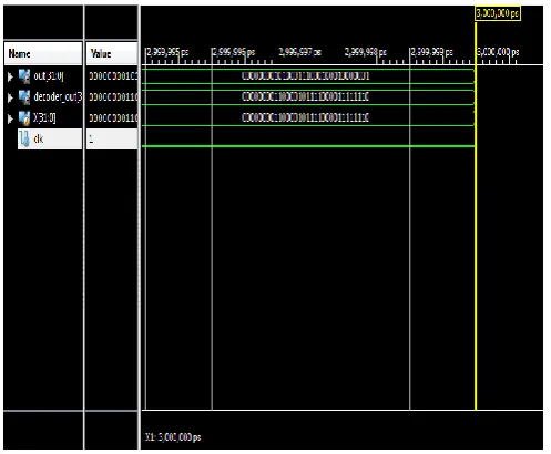
The proposed data encoding and decoding schemes are simulated and verified using Verilog HDL in Xilinx ISE 14.7.
[image:4.595.312.555.155.283.2]Scheme I
Fig 7 below shows the simulation output of encoding and decoding logic.
Fig 7: simulated output of scheme I encoding and decoding.
[image:4.595.312.557.376.517.2]Scheme II
Fig 9 below shows the simulation output of encoding and decoding logic and Ty, T2, T4** transition output.
Fig 9: simulated output of scheme I encoding and decoding.
Scheme III
Fig 9 below shows the simulation output of encoding and decoding logic and Ty, T2, T4** transition
Fig 9: simulated output of scheme I encoding and decoding.
4. CONCLUSION
[image:4.595.38.287.458.663.2]© 2016, IRJET | Impact Factor value: 4.45 | ISO 9001:2008 Certified Journal
| Page 2946
ACKNOWLEDGEMENT
I express my sincere thanks to Mr.Rohit P., Assistant Professor, Department of Electronics and Communication Engineering. Rajeev Institute of Technology, Hassan for his valuable guidance and continuous encouragement in course of my work. I would also like to thank Mrs. Ambika K. Head of the department, assignment professor, department of Electronics and Communication, Rajeev Institute of technology.
REFERENCES
[1] Nima Jafarzadeh, Maurizio Palesi, Ahmad Khademzadeh, and Ali Afzali-Kusha,”data encoding techniques for reducing energy consumption in network on chip” IEEE transactions on very large scale integration (vlsi) systems, vol. 22, no. 3, march 2014.
[2] M. Ghoneima, Y. I. Ismail, M. M. Khellah, J. W. Tschanz, and V. De, “Formal derivation of optimal active shielding for low-power on-chip buses,” IEEE Trans.
Comput.-Aided Design Integr. Circuits Syst., vol. 25, no. 5, pp. 821–
836, May 2006.
[3] Z. Yan, J. Lach, K. Skadron, and M. R. Stan, “Odd/even bus invert with two-phase transfer for buses with coupling,”
in Proc. Int. Symp. LowPower Electron. Design, 2002, pp.
80–83.
[4] Z. Khan, T. Arslan, and A. T. Erdogan, “Low power system on chip bus encoding scheme with crosstalk noise reduction capability,” IEE Proc. Comput. Digit.
Tech., vol. 153, no. 2, pp. 101–108, Mar. 2006.
[5] C. G. Lyuh and T. Kim, “Low-power bus encoding with crosstalk delay elimination,” IEE Proc. Comput. Digit.
Tech., vol. 153, no. 2, pp. 93–100, Mar. 2006.
[6] L. Rung-Bin, “Inter-wire coupling reduction analysis of bus-invert coding,” IEEE Trans. Circuits Syst. I, Reg.
Papers, vol. 55, no. 7, pp. 1911–1920, Aug. 2008.
BIOGRAPHIES
Asha J., pursuing M.Tech in VLSI designing and embedded systems in Rajeev institute of technology, Hassan, Karnataka, India.
Email: [email protected]
Rohith P. assistant professor, dept. of Electronics and communication, Rajeev institute of technology, Hassan, Karnataka, India.