© 2016, IRJET | Impact Factor value: 4.45 | ISO 9001:2008 Certified Journal
| Page 2408
Microcontroller Based Single-Phase Seven-Level Inverter
For Photo-Voltaic System
Ruhina R. Shaikh, Prof. J.R. Rana
Student, M.E(E.P.S), Jawaharlal Nehru Engineering College, [email protected]
Assistant Prof. Dept. of EEP, Jawaharlal Nehru Engineering College, [email protected]
Abstract
: The given paper presents the hardware design and implementation micro-controller based single phase seven level inverter for Photo- Voltaic application. The input to the given inverter is a DC source (Vdc) and it is capable of producing output of seven level (Vdc, 2Vdc/3, Vdc/3, 0, -Vdc, -Vdc/3, -Vdc/3). The switching devices used are IRF840 MOSFET and diodes. Control circuit for implementing the H-bridge inverter is done by using the micro-controller. The system proposed in given paper is having lesser number of switching devices which reduces the complexity of the circuit and a simple control circuit is employed using the micro-controller. The multi level inverters provides nearly sinusoidal output waveform, output current with refined harmonic profile and switching losses that are less than the conventional two level inverter and hence smaller filter size is required. The main application of this system is directly delivering the Photovoltaic generated energy to the power system networks by using this seven level inverter (SLI) as grid connected inverters.key words: multi-level inverter (MLI), pulse width
modulation (PWM), Seven level inverter (SLI), total harmonic distortion (THD), H-bridge, DC source (Vdc).
1. INTRODUCTION
In the last few years, new energy sources have proposed and developed due to the dependency and constant increase of costs of fossil fuels. On other hand, fossil fuels have a huge negative impact on the environment. In this context, the new energy sources are essentially renewable energies. It is estimated that the electrical energy generation from renewable sources will increase from 19%, in 2010, to 32%, in 2030, leading to a consequent reduction of CO2 emission [1]. Among these renewable energy sources, solar photovoltaic energy is one of the fastest growing.
In photo voltaic systems, solar energy is converted into electrical energy by photovoltaic (PV) arrays. PV arrays are very popular since they are clean, inexhaustible and require little maintenance. Photovoltaic systems require interfacing power converters between the PV arrays and the grid. Photovoltaic-generated energy can be delivered to power system networks through grid-connected inverters. A single-phase grid-grid-connected inverter is usually used for residential or low-power applications of power ranges that are less than 10 kW [2].
A multi level inverter is a power electronic device which is capable of providing desired alternating voltage levels at the output using multiple DC voltage as input. Various topologies for multilevel inverters have been proposed over the years [3]. Multilevel inverters are very promising; they have nearly sinusoidal output-voltage waveforms, output current with better harmonic profile, less stressing of electronic components owing to decreased voltages, switching losses that are lower than those of conventional two-level inverter and hence a smaller filter size is required, and lower EMI, all of which make them cheaper, lighter and more compact [4]-[5]. Common topology used are diode-clamped [6]-[11], flying capacitor or multi-cell [12]-[18], cascaded H-bridge [19]-[23], and modified H-bridge multilevel[24]-[27]. The concept of multi level inverter is kind of modification of conventional two level inverter. In multi level inverter we do not have to deal with the two level instead in order to create a smoother output waveform, more than two voltage levels are combined together.
Multilevel inverters produce a stepped output phase voltage with a refined harmonic profile when compared to a two-level inverter. The concept of multilevel inverters, introduced about 30 years ago, entails performing power conversion in multiple voltage steps to obtain improved power quality, lower switching losses, better electromagnetic compatibility, and higher voltage capability.
© 2016, IRJET | Impact Factor value: 4.45 | ISO 9001:2008 Certified Journal
| Page 2409
inverter used in power stages have the enhancement of theless switching devices and compact design as compare to other design of the existing seven level inverter circuit. Fig. 1 shows the block diagram of the single phase seven level inverter.
FIG.1 Block Diagram
The input is taken from the Photo Voltaic panel of 10 W which is having rated voltage of 17.85 V . The input to the multi level inverter should be different valued DC sources and for this purpose the capacitor voltage divider circuit is employed. The divider circuit will produce different voltage levels across it. And for seven level output we need three different DC input as per the rule of 2n+1, where 'n' is no. input DC sources.
The structure of this paper is organized as follows. The introductory part is covered in section I. The power circuit configuration is presented in section II. Then, the power circuit operation including the modes of operation in detail is discussed in section III. Experimental validation is described in section IV. Last section concludes and the scope for further work is presented.
2. POWER CIRCUIT
The power circuit is consisting of the rectifier, filter, capacitor voltage divider circuit, auxiliary switches and H bridge inverter. Fig. 2 shows the power circuit.
FIG.2 Power Circuit
2.1. Power Circuit Description
A single- phase seven-level inverter (SLI) power circuit was fabricated using six N-Channel enhancement mode MOSFET modules type IRF840 from Fairchild semiconductor. The MOSFET has advantage of nanosecond switching speeds, lesser power requirement and absence of secondary breakdown phenomenon. The capacitor voltage divider circuit is made by using the capacitor C1, C2 and C3 and each having value of 0.1 µf. Across each capacitor we will get the Vdc/3 volts.
2.2. Power Circuit Advantages
The advantages are as stated below:
1) Smaller filter size required, Improved output waveform
2) Lower electromagnetic interference (EMI) and total harmonic distortion (THD).
© 2016, IRJET | Impact Factor value: 4.45 | ISO 9001:2008 Certified Journal
| Page 2410
3. POWER CIRCUIT OPERATION
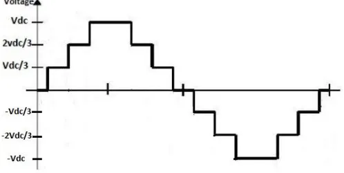
The given single phase multi level inverter is capable of producing seven level (Vdc, 2Vdc/3, Vdc/3, 0, −Vdc, −2Vdc/3, −Vdc/3) in output from the single DC source (Vdc) in the input.
FIG.3 Output Of Single Phase Seven Level Inverter
A. Mode I operation: Maximum positive output (Vdc) S1is ON connecting the load positive terminal to Vdc, and S3 is ON connecting the load negative terminal to ground. All other controlled switches are OFF; the voltage applied to the load terminals is Vdc.
B.Mode II operation: Two-third positive output (2Vdc /3) the auxiliary switch S5 is ON, connecting the load positive terminal, and S3 is ON, connecting the load negative terminal to ground. All other controlled switches are OFF; the voltage applied to the load terminals is 2Vdc/3.
C. Mode III operation: One-third positive output (Vdc/3) the auxiliary switch S6 is ON, connecting the load positive terminal, and S3 is ON, connecting the load negative terminal to ground. All other controlled switches are OFF; the voltage applied to the load terminals is Vdc/3.
D. Mode IV operation: Zero output This level can be produced by two switching combinations; switches S3 and S4 are ON, or S1 and S2 are ON, and all other controlled switches are OFF; load terminal is a short circuit, and the voltage applied to the load terminals is zero.
E.Mode V operation: One-third negative output (−Vdc /3) the auxiliary switch S2 is ON, connecting the load positive terminal and S8 is ON, connecting the load negative terminal to ground. All other controlled switches are OFF; the voltage applied to the load terminals is −Vdc/3.
F. Mode VI operation: Two-third negative output (−2Vdc/3) the auxiliary switch S2 is ON, connecting the load positive terminal, and S7 is ON, connecting the load
negative terminal to ground. All other controlled switches are OFF; the voltage applied to the load terminals is −2Vdc /3.
G. Mode VII operation: Maximum negative output (−Vdc ) S2 is ON, connecting the load negative terminal to Vdc , and S4 is ON, connecting the load positive terminal to ground. All other controlled switches are OFF; the voltage applied to the load terminals is –Vdc.
The given table shows in what sequence the switching devices should be switch ON and OFF in order to get the desired seven level output.
TABLE-1: Switching Combination For Seven Level Output
Vo
S1
S2
S3
S4 S5 S6
S7 S8
Vdc
ON Off ON Off Off Off Off Off
2Vdc/3
Off Off ON Off ON Off Off Off
Vdc/3
Off Off ON Off Off ON Off Off
Off
ON Off ON Off Off Off Off Off
-Vdc/3
Off ON Off Off Off Off Off ON
-2Vdc/3
Off ON Off Off Off Off ON Off
-Vdc
Off ON Off ON Off Off Off Off
4. EXPERIMENTAL VALIDATION
The experimental validation includes the photo voltaic panel details, control circuit, Driver Circuit , power circuit.
4.1. Photo Voltaic Panel details
[image:3.612.38.287.184.309.2]Photo voltaic panel of 10 watt is used as the input to the inverter circuit. Following table provides the detail:
TABLE 2 : PV Module Characteristics
Sr.No Parameter Rating
1 Max Power 10 W
2 Short Circuit Current 0.69 A
3 Open Circuit Voltage 21.65 V
4 Rated Voltage 17.85 V
5 Rated Current 0.62 A
.
4.2. Control Circuit
[image:3.612.320.592.279.426.2]© 2016, IRJET | Impact Factor value: 4.45 | ISO 9001:2008 Certified Journal
| Page 2411
using the "C" language. Criteria for choosing the PIC microcontroller is as follows:
1) Meeting the computing needs of the task at hand efficiently and cost effectively.
2) Availability of software development tools such as compilers, assemblers and debuggers.
3) Wide availability and reliable sources of the PIC micro controller.
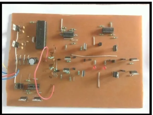
4.3. Driver Circuit
The driver circuit describes about the isolation between the power circuit and the control circuit and the power supplied to the MOSFETs. L293D a 16 pin IC is used as gate driver circuit. Operating voltage of 5 V is supplied through the 7805 voltage regulator IC. Four output terminals are available in L293D IC.
4.4. Power Circuit
A single phase seven-level inverter (SLI) power circuit was fabricated using six N-Channel enhancement mode MOSFET modules type IRF840 from Fairchild semiconductor. The MOSFET has advantage of nanosecond switching speeds, lesser power requirement and absence of secondary breakdown phenomenon.
FIG.4 Fabricated Circuit Of Single Phase Seven Level Inverter
All the technical details are given below:
Micro-controller : PIC16F877
Switching devices : MOSFET IRF840
Diodes (D1-D4) : 1N4007
Regulator IC : 7805, 7812
Capacitor values (C1,C2,C3) : 0.1 µF ceramic type
Driver circuit : L239D
5. EXPERIMENTAL RESULT
Photo voltaic panel of 10 watt is used as input to the inverter. The results are verified experimentally by using SLI circuit for 10W solar panel and tested with a resistive load of 10kQ and 10 W rating.
Figure.5 presents the output voltage waveform showing the desired seven voltage levels. The fundamental output frequency is 50Hz. The seven voltage levels are Vdc=12V, 2Vdc /3 = 8V, Vdc/3 = 4V, OV, Vdc/3 = 4V, -2Vdc/3 = -8V, -Vdc= -12 V. The results were taken from the experimental circuit using a two channel, 30 MHz, Cathode Ray Oscilloscope (CRO).
FIG. 5 Output Voltage Measured On Cro (Vertical: 3V/division, Horizontal: 5ms/division).
6. CONCLUSION
[image:4.612.332.567.364.553.2] [image:4.612.38.287.438.625.2]© 2016, IRJET | Impact Factor value: 4.45 | ISO 9001:2008 Certified Journal
| Page 2412
clearly that the single-phase SLI works as expected,generating the required seven-level output voltage from the PV array. A further development of the 1- phase SLI is able to be applied to any number of voltage levels for PV applications.
REFERENCES
[1] European Commission, EU Energy Trends to 2030, Luxembourg, Publications Office of the European Union, accessed on: http://ec.europa.eu/energy/observatory/trends_2030/".
[2] M. Calais And V. G. Agelidis, "Multilevel Converters For Single-Phase Grid Connected Photovoltaic Systems-An Overview,"1998, Vol. 1, Pp. 224 229.
[3] S. B. Kjaer, J. K. Pedersen, And F. Blaabjerg, "A Review Of Single-Phase Grid Connected Inverters For Photovoltaic Modules," IEEE Transaction On Industrial Appl., Vol. 41, No. 5, Pp. 1292-1306, Sep. L0 Ct. 2005.
[4] Y. Cheng, C. Qian, M. L. Crow, S. Pekarek, And S. Atcitty, "A
Comparison Of Diode-Clamped And Cascaded Multilevel Converters For A STATCOM With Energy Storage," IEEE Trans. Ind. Electron., Vol. 53, No. 5, Pp. 1512-1521, Oct. 2006
[5] P. K. Hinga, T. Ohnishi, And T. Suzuki, "A New PWM Inverter For Photovoltaic Power Generation System," In Conf. Rec. IEEE Power Electron. Spec. Conf-, 1994, Pp. 391-395.
[6] M. Saeedifard, R. Iravani, And L Pou, "A Space Vector Modulation Strategy For A Back-To-Back Five-Level HYDC Converter System," IEEE Trans. Ind. Electron., Vol. 56, No. 2, Pp. 452-466, Feb. 2009.
[7] S. Alepuz, S. Busquets-Monge, J. Bordonau, J. A. M. Velasco, C. A. Silva,J. Pontt, And L Rodriguez, "Control Strategies Based On Symmetrical Components For Grid-Connected Converters Under Voltage Dips," IEEE Trans. Ind. Electron., Vol. 56, No. 6, Pp. 2162-2173,Jun. 2009. [8] Rodriguez, J.S.Lai, And F.Z.Peng, " Multilevel Inverters: A Survey Of Topologies ,Controls And Applications," IEEE Trans. Ind. Electron., Voi.49,No.4,Pp.724-738, August 2002.
[9] J.Rodriguez,S.Bernet, B. Wu, Lo.Pont! And S.Kouro, "Multilevel Voltage-Source-Converter Topologies For Industrial Medium-Voltage Drives," IEEE Trans .Ind.Electron., Voi.54,No.6,Pp.2930-2945, Dec 2007. [10] M. M. Renge And H. M. Suryawanshi, "Five-Level Diode Clamped Inverter To Eliminate Common Mode Voltage And Reduce Dv/Dt In Medium Voltage Rating Induction Motor Drives," IEEE Trans. Power Electron., Vol. 23,No. 4, Pp. 1598-1160, Jul. 2008.
[11] E. Ozdemir, S. Ozdemir, And L. M. Tolbert, "Fundamental-Frequency Modulated Six-Level Diode-Clamped Multilevel Inverter For Three-Phase Stand-Alone Photovoltaic System," IEEE Trans. Ind. Electron., Vol. 56, No. 11, Pp. 4407-4415, Nov. 2009.
[12] R. Stala, S. Pirog, M. Baszynski, A. Mondzik, A. Penczek, J. Czekonski,And S. Gasiorek, "Results Of Investigation Of Multi Cell Converters With Balancing Circuit-Part I," IEEE Trans. Ind. Electron., Vol. 56, No. 7, Pp. 2610-2619, Jul. 2009.
[13] R. Stala, S. Pirog, M. Baszynski, A. Mondzik, A. Penczek, L Czekonski,And S. Gasiorek, "Results Of Investigation Of Multi Cell Converters With Balancing Circuit-Part 11," IEEE Trans. Ind. Electron., Vol. 56, No. 7, Pp. 2620-2628, Jul. 2009.
[14] P. Lezana, R. Aguilera, And D. E. Quevedo, "Model Predictive Control Of An Asymmetric Flying Capacitor Converter," IEEE Trans. Ind. Electron., Vol. 56, No. 6, Pp. 1839-1846, Jun. 2009.
[15] M. F. Escalante, J.-C. Vannier, And A. Arzande, "Flying Capacitor Multilevel Inverters And DTC Motor Drive Applications IEEE Trans. Ind. Electron., Vol. 49, No. 4, Pp. 809-815, Aug. 2002.
[16] A. Shukla, A. Ghosh, And A. Joshi, "Static Shunt And Series Compensations Of An SMIB System Using Flying Capacitor Multilevel Inverter," IEEE Trans. Power Electron., Vol. 20, No. 4, Pp. 2613-2622, Oct.2005.
[17] J. Huang And K. A. Corzine, "Extended Operation Of Flying Capacitor
Multilevel Inverter," IEEE Trans. Power Electron., Vol. 21, No. 1, Pp. 140--147, Jan. 2006.
[18] F.Z.Peng, "A Generalized Multilevel Inverter Topology With Self Voltage Balancing," IEEE Trans. Ind App/., Vol.37, No.2, Pp.611-617, Mar/April 2001.
[19] E. Villanueva, P. Correa, J. Rodriguez, And M. Pacas, "Control Of A Single Phase Cascaded H-Bridge Multilevel Inverter For Grid-Connected Photovoltaic Systems," IEEE Trans. Ind Electron., Vol. 56, No. II, Pp. 4399- 4406, Nov. 2009.
[20] L.M.Tolbert, F.Z.Peng, T.Cunnyngham And J.N.Chiasson, " Charge Balance Control Schemes For Cascade Multilevel Converter In Hybrid Electric Vehicles," IEEE Trans. Ind Electron., Vo1.49, No.5,Pp.1058- 1064, Oct.2002.
[21] K.A.Corzine, M.W.Wielebski, F.L.Peng And J.Wang, " Control Of Cascaded Multilevel Inverters," IEEE Trans. Power Electron., Vol.L9, No.3,Pp.732-738,May 2004.
[22] J. I. Leon, S. Vazquez, S. Kouro, L. G. Franquelo, J. M. Carrasco, And J. Rodriguez, "Uni-Dimensional Modulation Technique For Cascaded Multilevel Converters," IEEE Trans. Ind Electron., Vol. 49, No. 5, Pp. 1058-1064, Oct. 2002.
[23] C.-C.Hua, C.-W.Wu, And C.-W.Chuang, " A Digital Predictive Current Control With Improved Sampled Inductor Current For Cascaded Inverters," IEEE Trans. Ind. Electron., Vol. 56, No.5, Pp.1718-1726, May 2009.
[24] V. G. Agelidis, D. M. Baker, W. B. Lawrance, And C. V. Nayar, "A Multilevel PWM Inverter Topology For Photovoltaic Applications," In Proc. Leee , 1997, Pp. 589-594.
[25] S. J. Park, F. S. Kang,M.H.Lee, And C. U. Kim, "A New Single-Phase Five Level PWM Inverter Employing A Deadbeat Control Scheme," IEEE Trans .Power Electron., Vol. 18, No. 3, Pp. 831-843, May 2003.
[26] J.Selvaraj And N.A.Rahim, " Multilevel Inverter For Grid-Connected PV System Employing Digital PI Controller," IEEE Trans. Ind Electron., Vol. 56, No. I, Pp.149-159, Jan.2009.
[27] N.A. Rahim And J.Selvaraj. " Multi-String Five -Level Inverter With Novel PWM Control Scheme For PV Application," IEEE Trans. Ind Electron. , Vo1.57, No.6, Pp.2111-2121. June 2010.