Technology (IJRASET)
High Step-Up Converter Based On
Cockcroft-Walton Voltage Multiplier with Different
Capacitor Configuration
Sheeja G1, Reshma M2, Pranav M S31,2,3
M.Tech., Department of EEE, Vidya Academy Of Science And Technology, Thrissur, India
Abstract— Demand for electrical energy and concern about green energy evoke research in the renewable energy sources for electrical power production. Since the output of major renewable energy sources like solar and fuel cell is a low voltage DC, a step-up DC-DC converter plays a major role in renewable energy applications. Transformer less step-up converter based on Cockcroft-Walton voltage multiplier, proposed by Chung-Ming Young et. al, dealt with the computation of gain with capacitors all are equal. Objective of this paper is to analyse different capacitor combination in the step-up converter with Cockcroft- Walton voltage multiplier topology. A seven stage converter of 1kW rating is designed for different capacitor configurations. For validation, simulation is carried out for both equal capacitors and different capacitors configurations. From low-input-level renewable energy sources, the proposed converter provides a high DC voltage at relatively low cost. This converter is suitable for various applications to boost the DC voltage in a cost effective manner.
Keywords— High gain step-up converter, Cockcroft-Walton voltage multiplier, Transformer-less boost converter, Voltage ripple reduction, Low voltage stress, Various capacitor configuration of CWVM, Low current ripple.
I. INTRODUCTION
ELECTRIC power is an issue that touches almost every person on the planet and the demand for electrical energy increases day-by-day. Renewable energy sources especially fuel cell and solar cell attract the researchers and the government all over the world. Because of low level voltage generation, a high gain dc-dc converter is required in the power conversion systems corresponding to these two sources.
A. Boost Converter
Technology (IJRASET)
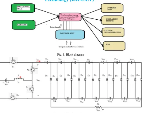
[image:3.612.81.544.69.437.2]Fig. 1. Block diagram
Fig. 2. CW voltage multiplier based stepup converter.
B. General Applications
Step-up converter based on CWVM is suitable for various applications especially where high voltage gains are desired. It can be directly applied for numerous applications; some of them are listed below.
Equipments in telecom sector uses a 48V bus distributed power system which has a backup of 48V dc battery plant. The information industry uses uninterruptable power supplies, but the backup time provided by them is not enough; a better choice for providing longer reverse time is to use the 48V telecom power supply and to boost it to 380-V intermediate dc bus.
Most of the industrial electrical equipments and commercial power systems are operating in 50 Hz AC. So use of an AC source for insulation testing seems to be the logical choice. Since insulation systems are extremely capacitive and AC test equipments are bulky, DC test equipment is considered to be more suitable than AC. For testing a cable of one-mile length at 50 kV AC would require an equipment of 500 kVA capacity . A DC test at 50 kV would require an equipment of 50 W capacity.
In fuel cell vehicle, step-up converter is employed to provide an input to the inverter which in turn supplies the AC loads. Output from the boost converter of n stage can be utilized for all AC applications by connecting a suitable inverter of n+1 level. Thus application of step-up converter has been spreading in every corner of residential, electric transportation, electrical testing, space and utility systems. A block diagram showing some of the applications is depicted in fig.1
C. Organisation
Chapter II discuss with operation Cockcroft-Walton voltage multiplier based step-up converter. Chapter III deals with the design of the seven stage converter.
Technology (IJRASET)
In chapter VI, future works to be done in this area is discussed.
II. CIRCUITDESCRIPTION
Proposed converter is an integration of a conventional boost converter and voltage multiplier as shown in the fig.2
A. Circuit Components
Supply: A low-level dc source, such as battery, PV array or fuel cell sources One boost inductor L, four MOSFET switches (S1,S2, S3 and S4)
One n-stage Cockcroft-Walton voltage multiplier.
The input voltage and current are represented by Vdc and IL respectively ; the output voltage is denoted by Vout, and the output
resistor is represented by Ro.
1) Source: Supply is obtained from a DC source of 40V which can be obtained from renewable energy soures or battery.
2) Switches: S1(S2) and S4(S3) operate in complementary mode, and the operating frequencies of S1 and S2 are termed as fmod
and falt respectively. fmod is the modulation frequency and falt is the alternating frequency; fmod is set much higher than falt. High
[image:4.612.195.424.292.453.2]frequencies are selected so that smaller inductor and capacitors can be used. Regulation of output voltage is done by controlling the duty cycle of S1 and S4, while the output voltage ripple can be adjusted by falt.
Fig. 3. Output voltage of CW voltage multiplier circuit
3) Cockcroft-Walton Voltage Multiplier: In the circuit shown in the fig.2, the subsequent stage is a Cockcroft-Walton Voltage Multiplier. One of the cheapest and popular ways of generating high voltages at low currents is the multistage diode-capacitor voltage multiplier also known as Cockcroft- Walton multiplier.(Proposed by James Douglas Cockcroft and Ernest Thomas Sinton Walton). Merit of such circuit is that the voltage across each stage is only equal to twice the peak input. Thus size and cost of the components can be reduced to a great extent. Output can be tapped from any stage like a multi-tapped transformer. In CW voltage multiplier, each stage has two capacitors and two diodes. In Cockcroft-Walton voltage multiplier of n-stage , the number of diodes and capacitors will be of 2n. For no load, the output voltage will be of 2n times of input. The output voltage and ripple of a Cockcroft-Walton voltage multiplier is shown in the fig.3.
B. Assumptions
In the fig.2, Vac represents terminal voltage and iac represents the current of the cascade Cockcroft-Walton voltage multiplier circuit.
The reference direction is indicated in the fig.2. The capacitors and diodes are denoted by Ci and Di respectively.
For the simplification of analysis, it is assumed that
The converter in fig.2 is operating in steady state and continuous conduction mode. All the components are ideal and thus the circuit has 100% efficiency
Technology (IJRASET)
C. Circuit Operation
By using the switches S1, S2, S3 and S4, the input DC voltage is converted into alternating waveform. Moreover the boost inductor, L boosts the input voltage of the CCW voltage multiplier circuit. The forward biasing of diode depends upon the charge of the capacitors to which the particular diode is connected. Only one of the diodes in the CW circuit will conduct when ICW > 0. Sequence
of conducting diode is from right to left with even diodes conducting in positive half cycle and odd diodes conducting in negative half cycle. The condition for the conduction of each diode is determined by the terminal current ICW and capacitor voltages Vc1 to
Vc14. The boosted dc voltage is available across the load which is connected across the even capacitors.
D. Modes Of Operation
During positive half cycle of the alternating waveform, only one of the even diodes conducts with the sequence D14, D12, D10, D8, D6, D4 and D2 and that the even (odd) capacitors gets charged (discharged) through the conducting diodes. The characteristic behavior of each mode in the positive half cycle is explained by using the fig.4 to fig.11.
1) MODE-1:During the first mode, S1 and S2 turn on whereas S3, S4 and all diodes are in off condition. Energy stored in the inductor increases. Even group capacitors C14, C12, C10, C8, C6, C4, and C2 supply the load. Odd-group capacitors C13, C11, C9, C7, C5, C3, and C1 are floating.
2) MODE II: During the second mode, S2 and S4 turn on whereas S1, S3 and all diodes except D14 are in off condition. Thus, in this stage, even group capacitors C2i for every i є [1,7] fed the load. while the input voltage Vdc , inductor and the odd group
[image:5.612.59.562.286.693.2]capacitors C2i-1 for every i є [1,7] charge the even group capacitors.
Fig. 4. I Mode of operation
Fig. 5. II Mode of operation
Technology (IJRASET)
voltage Vdc , inductor and odd group capacitors C2i-1 for every i є [1,6] charge the even group capacitors.
4) MODE-IV TO VIII: Switches S1, S2, S3 and S4 remain in the same state. Diode conduction is shown in the fig.7 to 11. Thus at the end of eighth mode, energy gets transfered from supply side to load. Behavior of the circuit is similar during the negative half cycle of the alternating waveform. The odd diodes are conducting with the sequence D13, D11, D9, D7, D5, D3, and D1. Moreover the odd capacitors are charged and even capacitors are discharged. The behavior of the CW circuit during the positive and negative half cycle can be obtained through eight modes of operation each. Inductor gets charged when S3 & S4 are closed and discharges while S1 and S3 are conducting.
III. DESIGN CONSIDERATIONS
A. Design
The analysis was carried out for three stage step-up converter in [3]. Design of inductance, capacitance and resistance are based on expressions in [3].
Gain of the converter depends on number of stages and duty ratio of the modulating switches. = (1)
Voltage stress across the first capacitor is half the stress across other capacitors.
1 = (2)
= for i = 2; 3... 2n (3)
Maximum current stress across the switches and diodes are equal to the peak value of the inductor current. Ipk
Maximum voltage stress across the switches and diodes depends on output voltage and number of stages.
Design of input Inductance is based on input current, ripple current and operating frequency of the modulating switches.
= ∗ (4)
[image:6.612.50.548.208.624.2]= ∗ (5)
Technology (IJRASET)
Fig. 7. IV Mode of operation
Fig. 8. V Mode of operation
Fig. 9. VI Mode of operation Load resistance
= (6)
Technology (IJRASET)
= ( )
∗ (7)
Output voltage ripple is equal to the sum of all even capacitor voltage ripples;
= (8)
Where,
Vdc Input voltage
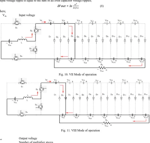
[image:8.612.50.544.101.571.2]Fig. 10. VII Mode of operation
Fig. 11. VIII Mode of operation
Vout Output voltage
n Number of multiplier stages D Duty ratio of switch sm1
K Percentage of the peak-peak ripple current Vck Steady state voltage of the kth capacitor.
Po Output power Vout Output voltage ripple
fsc Operating frequency of switches sci
Technology (IJRASET)
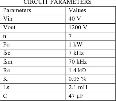
TABLE I
CIRCUIT PARAMETERS
. B.Circuit specification
In this work, a seven stage converter is considered and the input voltage of 40 V is boosted to 1200 V. Selected parameters and the designed component values are tabulated in Table.I
IV.SIMULATION ANALYSIS
The impact of different combinations of capacitors are determined by conducting simulation studies on the seven stage converter using MATLAB/SIMULINK software. Simulation diagram is shown in the Fig.12. The simulation is done for three different configuration of capacitors.
A. Case-i:C2i=Ci=C
In this case, all the capacitors of Cockcroft-Walton voltage multiplier are of same value. Designed value of base capacitance is 47µF. The output voltage ripple is around 66 V (i.e.) 5.5 % of voltage ripple is present in the output voltage of 1200 V. The inductor current has a ripple of around 350 mA. The gain of the converter is around 28.75
B. Case-ii: C2i=Ci=C & C1=2C
In this case, the first capacitance is considered to be twice than that of others. Here C1 = 94 µF and Ci = 47 µF for every i = 2,3..2n. The output voltage ripple is around 64 V (i.e.) 5.33 % of voltage ripple is present in the output voltage. The inductor current has a ripple of around 350 mA. The gain of the converter is around 29.7.
Fig. 12. Simulation circuit
C. Case-iii: C2i=Ci=(n-i+1)C
Parameters Values
Vin 40 V
Vout 1200 V
n 7
Po 1 kW
fsc 7 kHz
fsm 70 kHz
Ro 1.4 kΩ
K 0.05 %
Ls 2.1 mH
[image:9.612.95.515.503.687.2]Technology (IJRASET)
Here, the capacitance of each stage differs from other stages. Here the value of capacitor depends on that particular stage number. C1 = C2 = 329 µF
C3 = C4 = 282 µF C5 = C6 = 235 µF C7 = C8 = 188 µF C9 = C10 = 141 µF C11 = C12 = 94 µF C13 = C14 = 47 µF
[image:10.612.185.367.211.445.2]The output voltage ripple is around 16 V (i.e.) 1.33 % of voltage ripple is present in the output voltage. The inductor current has a ripple of around 180 mA. The gain of the converter is around 30.375.
Fig. 13. Output voltage
D. Comparison Of Different Capacitor Configuratons
From the fig.13, it is observed that the voltage ripple in caseiii is lesser than that of case-i and ii. Moreover the ripple content in input current is also reduced as shown in the fig.14. It is also observed that different capacitor combination has impact in gain of the converter. Thus overall performance of the converter is improved while using different capacitors(C2i=Ci=(ni+1)C) at different stages of the multiplier section.
[image:10.612.223.388.525.709.2]Technology (IJRASET)
V. CONCLUSION
A step-up converter based on seven stage Cockcroft-Walton voltage multiplier is analysed. Converter with three different capacitor combinations are designed and simulated. The impact of different capacitor configuration on output voltage ripple, input current ripple and gain of the converter is analysed. Impact of different capacitor combination is more pronounced as the number of multiplier stages increases. Thus converter performance has been improved by using different capacitor combination. Thus voltage multiplier based step-up converter provides a cost effective solution for high voltage requirements. The proposed configuration has a few short comings like overshoot that need to be addressed to make it robust and applicable for all the systems.
REFERENCES
[1] E. Kufel, W.S. Zaengl, HV Engineering-Fundamental, 2nd Edition 2000, publisher- Butterworth-Heinemann
[2] Muhammed H Rashid, Power Electronics Circuits, Devices & Applications, 3rd Edition
[3] Chung Ming Young, Ming Hui Chen, Chun Cho Ko, Kuo Kuang Jen & Tsun An Chang, ”Cascade Cockcroft Walton Voltage Multiplier Applied to
Transformer less High StepUp DC DC Converter” IEEE Transactions On Industrial Electronics, Volume. 60, Number 2, February 2013.
[4] Wai R. J., Duan R. Y.,Lin C. Y. & Chang Y. R.-2007 ”High Efficiency DC DC Converter with high voltage gain & reduced switch stress” IEEE Transaction
Ind. Electron., volume. 54, number. 1, pp. 354-364.
[5] I C Kobogias & E C Tatakis, ”Optimal design of a half-wave CW voltage multiplier With Minimum Total Capacitance” in IEEE Transaction- Power
Electronics, volume. 25, no: 9, pp. 2460-2468, Sep-2010.
[6] Yang L. S., Liang T. J. & Chen J. F.-2009, “Transformer-less DC DC converter with high step up voltage gain”, IEEE Transaction Ind. Electron., volume 56,