© 2017, IRJET | Impact Factor value: 5.181 | ISO 9001:2008 Certified Journal | Page 1387
Software Design of Digital Receiver using FPGA
G.C.Kudale
1, Dr.B.G.Patil
2,K. Aurobindo
31
PG Student, Department of Electronics Engineering, Walchand College of Engineering, Sangli, Maharashtra,
2
Associate Professor, Department of Electronics Engineering, Walchand College of Engineering,
Sangli, Maharashtra ,India,
3
Scientist-’D’,S.A.M.E.E.R, IIT-Bombay Powai(W), Mumbai, Maharashtra, India
---***---Abstract
– In the past radio receivers were designed withanalog circuitry but for overcoming the disadvantages of analog circuitry now all becomes all digitized. So Wireless communication have a great demand in today’s world. The digital receiver must be communicated with all the new wireless standards. In RADAR obtaining the information from target devices digital receivers are used. In this proposed paper 70MHz with Doppler taken from digital receiver and ADC sample this analog signal with high sampling rate. Sampling technique is used for this is band pass sampling i.e. under sampling. For minimization of sampling rate in digital there is digital down converter (DDC) which is used for frequency translation and better decimation factor. After this process we got a signal which have higher precision and more stability and it’s become very easy to collect information from target. This entire architecture digital receiver is implemented in Xilinx IP Core and is captured on FPGA (Spartan 6 SP601) interfaced with ADC (LTC 2107) via FMC connector.
Key Words: Digital Receiver, ADC (DC2266A), Field Programmable Gate Array (FPGA), Spartan 6 SP601, Digital Clock Manager (DCM), Digital down converter, Digital filter.
1. INTRODUCTION
In order to overcome the disadvantages of the Analog Receivers like low noise immunity, Component Aging, Temperature Variation, Calibration, Requirement of specific H/W and S/W etc. the digital receiver came into picture
.
This project focuses on the design and implementation of a digital receiver using FPGA. With the main components of the receiver being the Anti-Aliasing Filter to remove the Aliasing effect, High speed A/D Converter (LTC2107) by Linear Technology and an ADC Driver (LTC6409) again by Linear Technology which is sampled using Band pass Sampling whose output is then fed to the Mixer which performs the frequency translation and is given to the Decimating Low-Pass Filter which converts the signal in I and Q format which via the Ethernet is mapped on a Monitoring system and various parameters for a CLOUD RADAR can be recorded. Direction finding is an ideal application for digital receivers because of their excellent channel-to-channel phase matching and consistent delay characteristics. Radar applications benefit from the tight coupling of the A/D, digital receiver and DSP functions to processwideband signals. FPGAs are especially well suited to handle FFT and pulse compression tasks normally required in the signal processing sections [1].
This paper shows how digital receivers, the fundamental building block for software radio, can replace conventional analog receiver designs, offering significant benefits in performance, density and cost.
2. System Description and Theory
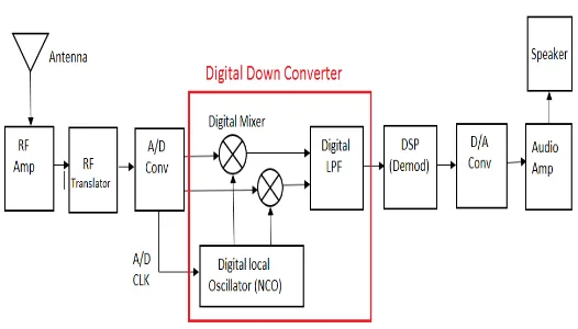
Looking at the overall block diagram, the digital samples coming out of the A/D converter are being fed to the next stage which is the digital receiver chip-in the red line, as shown in Fig.1. The digital receiver chip is typically contained on a single monolithic chip which forms the heart of the digital receiver system. It is also sometimes referred to as a digital down converter (DDC) or a digital drop receiver (DDR) [2].
Fig -1: Digital Receiver block diagram
Inside the digital down converter there are three major sections:
Local Oscillator Digital mixer
Decimating low pass filter
[image:1.595.309.572.470.620.2]© 2017, IRJET | Impact Factor value: 5.181 | ISO 9001:2008 Certified Journal | Page 1388 this in DDC local oscillator i.e. Numerically controlled
oscillator is generates digital samples of two sine waves precisely offset by 90 degrees in phase, creating sine and cosine signals. The digital samples out of the local oscillator are generated at a sampling frequency exactly equal to the A/D sample clock frequency, fs 60MSPS.The next major component of the digital receiver chip is the Mixer which consists of two digital multipliers. Digital input samples from the A/D are mathematically multiplied by the digital sine and cosine samples from the local oscillator. The data rates into both inputs of the mixers are the A/D sampling rate fs, the multipliers also operate at that same rate and produce multiplied output product samples at fs i.e.60MSPS.The sine and cosine inputs from the local oscillator create I and Q (in-phase and quadrature) outputs that are important for maintaining phase information contained in the input signal.
Fig -2: Digital down Converter
Once the RF signal has been translated, it is now ready for filtering. The decimating low Pass filter accepts input samples from the mixer output at the full A/D sampling frequency fs. It utilizes digital signal processing to implement an FIR (Finite Impulse Response) filter transfer function. The filter passes all signals from 0 Hz up to a programmable cut off frequency or bandwidth, and rejects all signals above that cut-off frequency. This digital filter is a complex filter which processes both I and Q signals from the mixer. At the output you can select either I and Q (complex) values or just real values, depending on your system requirements. So at the output of DLPF we get low frequency output at 1MSPS having 60 decimation factor [2].
3. Proposed Digital Receiver
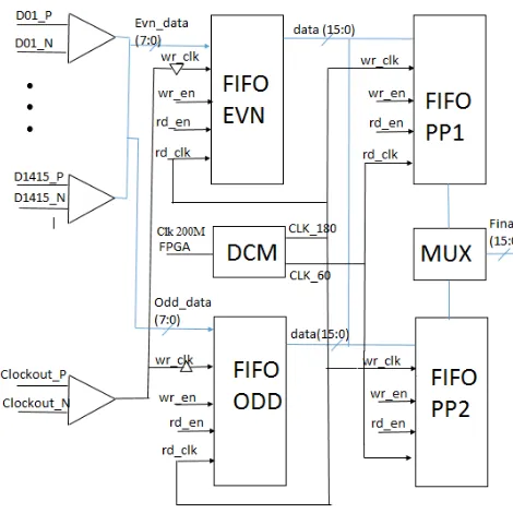
Fig -3: Acquiring the Digital Signals from the ADC
In fig.3. analog input is driven by an ADC driver LTC6409) which converts the single ended input to differential output which is then fed in the ADC (LTC2107)giving 16-bits digital LVDS signal at the output [3].
[image:2.595.326.561.125.360.2] [image:2.595.69.280.329.493.2]© 2017, IRJET | Impact Factor value: 5.181 | ISO 9001:2008 Certified Journal | Page 1389 signals. This raw I and Q signals are then passed through
the decimating low pass filter to bring down the sampling rate 1MSPS by decimating it by a factor of 6[4].
3.1 Band pass Sampling
Although satisfying the majority of sampling requirements, the sampling of low pass signals is not the only sampling scheme used in practice. We can use a technique known as band pass sampling to sample a continuous band pass signal that is centered about some frequency other than zero Hz. Acceptable range of frequencies for Band-Pass Sampling can be calculated as following formula.
If we use the sampling frequency less than twice the maximum frequency component in the signal, then it is called under sampling. Under sampling is also known as band pass sampling, harmonic sampling or super-Nyquist sampling. Nyquist-Shannon Sampling theorem, which is the modified version of the Nyquist sampling theorem, says that the sampling frequency needs to be twice the signal bandwidth and not twice the maximum frequency component, in order to be able to reconstruct the original signal perfectly from the sampled version. If B is the signal bandwidth, then Fs > 2B is required where Fs is sampling frequency. The signal bandwidth can be from DC to B or from f1 to f2 where B = f2 – f1 [5].
3.2 Interfacing of ADC to FPGA
The ADC chip selected supports SPI. Serial Programming Mode to use the Serial Programming Mode, PAR/SER should be tied to ground. The SS, SCLK, MISO and MOSI pins become a serial interface that program the A/D mode control registers. Data is written to a register with a 16-bit serial word. Data can also be read back from a register to verify its contents. Serial data transfer starts when SS is taken low. The data on the MOSI pin is latched at the first 16 rising edges of SCLK. Any SCLK rising edges after the first 16 are ignored. The at transfer ends when SS is taken high again. The first bit of the 16-bit input word is the R/W 16-bit. The next seven 16-bits are the address of the register (A6:A0). The final eight bits are the register data (D7:D0). If the R/W bit is low, the serial data (D7:D0) will be written to the register set by the address bits (A6:A0). If the R/W bit is high, data in the register set by the address bits (A6:A0) will be read back on the MISO pin (see the Timing Diagrams).During a read
back command the register is not updated and data on MISO is ignored[4].
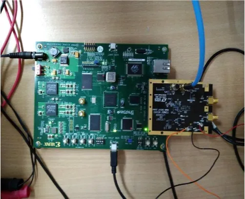
3.3 Hardware Setup
ADC evaluation board is connected to FPGA SP601 via FMC LPC connector. FPGA Mezzanine Card (FMC) is an ANSI/VITA standard that defines I/O mezzanine modules with connection to an FPGA or other device with re-configurable I/O capability. It specifies a low profile connector and compact board size for compatibility with several industry standard slot card, blade, low profile motherboard, and mezzanine form factors.
Fig -4: Hardware Setup
3.4 Digital Clock Manager (DCM)
Clocking Wizard helps create the clocking circuit for the required output clock frequency, phase and duty cycle using mixed-mode clock manager (MMCM) or phase locked loop (PLL) primitive. It also helps verify the output generated clock frequency in simulation, providing a synthesizable example design which can be tested on the hardware. It also supports Spread Spectrum feature which is helpful in reducing Electromagnetic interference.
4. RESULTS AND DISCUSSIONS
4.1 Programming the ADC using SPI
[image:3.595.308.559.276.480.2]© 2017, IRJET | Impact Factor value: 5.181 | ISO 9001:2008 Certified Journal | Page 1390 Fig -5: VHDL output to program the ADC
The SS, SCLK, MISO and MOSI pins become a serial interface that program the ADC mode control registers. The data transfer starts when SS is taken low. Data is written to a register with a 16-bit serial word. The data on the MOSI pin is latched at the first 16 rising edges of SCLK. The data transfer ends when SS is taken high again.
4.2 Digital Clock Manager (DCM)
DCM provides clocking to all the resources of Xilinx FPGA with advanced feature. Digital Clock Manager DCM integrates advanced clocking capabilities to FPGA global clock distribution network. It eliminates clock skew, Phase shifting, and also act as frequency synthesizer multiply/divide input clock. Input of DCM is 27MHz (on board clock) i.e. User clock which gives 60MHz 180MHz as output clock. DCM is generated in Xilinx IP core. VHDL output is shown in figure 6.
Fig -6: VHDL output of DCM
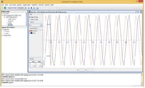
4.3 Acquired ADC output
The final data output from 16 bit FIFOs having Ping-Pong operation can be read from 60MHz clock.
Output will display on chip scope software of ISE 4.7 design suite. ADC output data coming from rising falling edges of CLKOUT+ which 60MHz frequency. Input of ADC is 70MHz with Doppler (Intermediate frequency) and sampled at 60MSPS sampling rate.
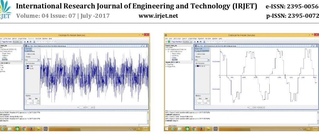
Fig -7: Acquired ADC Data 10.3MHz at 60MSPS
4.4 Direct Digital Synthesizer (DDS)
Data from the ADC will be multiplied withe the signals from the NCO. The NCO is tuned in such a way that it will produce two sine signals which are 90o out of phase with respect to each other. Here since the data from the ADC is timed at 10MHz and at 60Msps therefore the NCO will also generate signals at 10 MHz and at 60Msps.
Fig -8: Sine & Cosine generated at 10MHz and 60Msps
4.5 Digital Mixer
[image:4.595.37.290.66.256.2] [image:4.595.309.558.168.315.2] [image:4.595.308.559.464.616.2] [image:4.595.38.289.528.686.2]© 2017, IRJET | Impact Factor value: 5.181 | ISO 9001:2008 Certified Journal | Page 1391 Fig -9: I Signal 20.3M and 300K
4.6 Low Pass Filter
[image:5.595.46.557.46.261.2]The mixer output I and Q signals are then passed through the low pass filter to remove all the high frequency components. The Figure shows that only 300 KHz of I and Q signals that passes through low pass filter.
Fig -10: I Signal of 300K
Further processing of this signal is decimation. Above I and Q signals having 60MSPS sampling rate so foe system requirement it requires 1MSPS sampling rate. So by collecting 1 sample from 60 sample that becomes1MSPS sampling rate. In figure below show the signal of 500 KHz signal having 1MSPS sampling rate.
Fig -11: Decimated output at 1 MSPS
5. CONCLUSION
Benefits of using a Digital Receiver are Reduction of DSP processing demands, Very fast tuning, No PLL’S, Fast bandwidth selection, Zero frequency drift and error, Precise, stable filter characteristics, Excellent dynamic range, etc.
The Designing of the ADC Front-End Circuit is complete and the final fabricated board is also tested by interfacing it with the Spartan-6 Evaluation Board (SP601) via the FMC connector
.
REFERENCES
[1] Dr. M. Kamaraju, Jayaraju. D, FPGA Based 70MHz Digital Receiver, for RADAR Applications, International Journal of Research in Electronics Communication Technology Volume 1, Issue 1, July-September, 2013, pp. 01-07.
[2] Rodger H. Hosking,”Digital Receiver Handbook: Basics of Software Radio”, Fifth Edition Pentek.
[3] Linear Technology,”10GHz GBW, 1.1nV/p Hz Differential Amplifier/ADC Driver”, LTC6409 datasheet, 2010.
[4] Linear Technology,”16-Bit, 210Msps High Performance ADC”, LTC2107 datasheet, 2014.
[5] Richard G. Lyons, Understanding Digital Signal Processing, 3rd edition, Prentice, Hall, November 2010.
[6] Doglas Perry, VHDL Programming by examples, 4th Edition, McGraw-Hill Professional, July 2002
[image:5.595.38.288.387.550.2]