International Journal of Emerging Technology and Advanced Engineering
Website: www.ijetae.com (ISSN 2250-2459, ISO 9001:2008 Certified Journal, Volume 3, Issue 7, July 2013)
126
Analysis of Electrical Parameters of Inset Fed Rectangular
Micro strip Patch antenna (RMPA) by Varying Inset Gap and
Inset Width
Swarna Pundir
1, D. Arya
2, Aruna Bansal
3 1,3M.Tech Student, IET Alwar, Electronics and Communication Department
2Associate Professor, IET Alwar, Electronics and Communication Department.
Abstract-- This paper investigate the dependency of electrical properties of inset fed rectangular microstrip patch antenna (RMPA) by varying inset width and inset gap for proper impedance matching to achieve efficient operation. The design strategy is optimized for 2.4 GHz rectangular shaped patch antenna using CST Micro stripes 2009 EMC Edition. It has been observed the performance of patch antenna depends more on inset gap between patch conductor and inset fed line rather than inset length.
Keywords-- Inset- fed, Inset gap, Inset width, Inset fed Line, Patch antenna, Resonance frequency
I. INTRODUCTION
A wireless communication system emphasis on lightweight, compact and cost effective low profile antennas for frequencies above100 MHz (ʎ ˂ 3m). Microstrip patch antenna rises as a good candidate meeting these requirements due to its versatility of possible geometry and easy integrity with printed circuits. The performance of a patch antenna depends upon their geometrical shape, physical dimensions and properties of the material used. Including all this the location and type of feed also plays a vital role for improving its performances. The inset feed antenna provides a method of impedance control with a planer configuration [1-2].It is found that a shifted Cos2 function works well for the inset-fed patch [3-4]. The parameters of the shifted cosine function –squared depend on the inset width for a given patch and substrate geometry [5]. Bandwidth of a patch antenna is a linear function of substrate thickness t and increasing t to increase bandwidth result in greater surface wave, spurious radiation and reduced directivity. In inset fed technique a notch is cut on the edge of radiating patch to increase the matching for better performance by controlling the input impedance level.
This paper analyzes the variation of electrical properties of a patch antenna with respect to inset width and inset gap keeping the width of inset fed line constant.
II.DESIGN PROCEDURE
Before designing a Patch antenna we take consideration of some basic facts like resonant frequency fr, kind of
model used for analysis, feeding method, shape and dimensions of patch as well as substrate. So here the fr is
2.4 GHz ,Transmission line model is used because of ease and gives good physical insight yet has less accurate and it is more difficult to model coupling[6].Feeding method used is recessed microstrip-line feed, shape considered is rectangular patch on GML 1000 with dielectric constant εr
= 3.2 and thickness (t) of substrate is .762mm.
III. DESIGN METHODOLOGY
While adopting the design strategy we try to keep the return loss as minimum as possible. Design procedure is conventional based on existing literature, choosing εr in
advance as dielectric of substrate are not easily available which alongside also brings the thickness of the material with itself.
IV. PATCH ANALYSIS
Steps:
1. Calculate Width „W‟ [7]
√
2. Calculate εreff [9]
εreff =
+ [ ]
-1/2
for Wp / h>1
3. Calculate ΔL i.e. normalized length[8]
= 0.412 (
)
International Journal of Emerging Technology and Advanced Engineering
Website: www.ijetae.com (ISSN 2250-2459, ISO 9001:2008 Certified Journal, Volume 3, Issue 7, July 2013)
127
4. Calculate LP
=
√
- 2ΔL
5. For calculating notch width we use equation [10]
=
√
+
Rearranging the above equation for
= √
6. Calculating [11][12]
= ( )
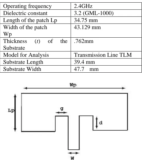
[image:2.612.48.289.367.639.2]Tabulated values using above equations are shown in Table 1.
Table 1:
Physical dimensions of microstrip patch antenna
Operating frequency 2.4GHz
Dielectric constant 3.2 (GML-1000) Length of the patch Lp 34.75 mm Width of the patch
Wp
43.129 mm
Thickness (t) of the Substrate
.762mm
Model for Analysis Transmission Line TLM Substrate Length 39.4 mm
Substrate Width 47.7 mm
Fig .1 shows the patch design with inset-fed located along the width.
V.SIMULATION STRATEGY
Simulation is carried in a way to find out the effect of variation in inset-fed gap and inset fed length on the electrical parameters of patch antenna. Feed line with a fixed width is extended up to the edge of the patch.
If we cut a notch on the patch and extend the inset fed line, the input resistance of the fed line is that of where the notch has been cut out of the patch, this gives a good impedance matching for better result.
Here two parameters i.e. Inset gap width (notch width) and the Inset fed (notch length) is varied keeping one of the parameter constant at a time. Starting from the non radiating edge notch width set to 00mm to0.34mm, 0.35mm and.5mm. Repeating it for the notch length from the calculated value of 7.5mm ± 0.5mm.The variation is kept in small steps as a minute change can also be easily observed in this process rather than using bigger variations.
VI. RESULT AND DISCUSSION
Summarizations of different model are shown in the Table 2, showing the effects on all the electrical parameters of microstrip patch antenna. Figure _and _ shows the simulated variation in return loss (S11) and
bandwidth for model C, G and K. As input impedance of inset fed patch antenna depends primarily upon the inset length „d‟ and to some extend at the inset gap between patch conductor and inset line. These result shows that the resonance frequency ,return loss and bandwidth is to some extend depends upon the inset gap ‟g‟ and less on inset length ‟d‟. On comparing model no A, E, I with C,G,K, it is easily seen that due to input impedance there is shift in S11
,bandwidth and resonance frequency . One can be precise
for a selective resonance frequency with choosing a proper width gap.
VII. CONCLUSION
For better analysis, input impedance of patch antenna plays an important role as it will decide the performance of an patch antenna. It can be easily concluded that impedance matching depends more on inset gap rather than inset length which in return affect the electrical parameters of a microstrip antenna.
REFRENCES
[1] L.I.Basilio,M.A.Khayat,J.T.Williams and S.A. Long, “The Dependence of the Input Impedance on Feed Position of Probe and Microstrip Line-fed Patch Antenna,”IEEE Trans.Antenna and Propagation,Vol.AP-49,pp.45-47,Jan.2001.
[2] T.Samaras,A.Kouloglou ,and J.N.Sahalos, “A note on the impedance variation with feed position of a rectangular microstrip antenna, ”IEEE Antennas and Propagation Magazine,vol.46,pp.90-92,April2004.
International Journal of Emerging Technology and Advanced Engineering
Website: www.ijetae.com (ISSN 2250-2459, ISO 9001:2008 Certified Journal, Volume 3, Issue 7, July 2013)
128
[4] Y.Hu, D.R. Jackson ,J.T.williams , and S.A.Long,”A Designapproach for inset-fed rectangular microstrip antennas,” AP-S International Symposium,pp.1494 july2006.
[5] M.A.Matin, A.I.Sayeed ,”A Design for Inset-fed Rectangular Microstrip Patch Antenna,” Wseas Transactions on Communication ,Issue 1,Vol.9,Jan 2010.
[6] E.H Van Lil and A.R Van De Capelle ,”Transmission –Line Model for Mutual Coupling Between Microstrip Antennas,” IEEETrans.Antennas Propagat.,Vol AP-32,No.8,pp816-821,Aug1984.
[7] I.J Bahl and P Bhartia, Microstrip Antenna, Artech House, Dedham.M.A, 1980.
[8] T.A.Milligan,Modern Antenna Design, McGraw-Hill Book Co., New York ,1985
[9] C.A.Balanis, Advanced Engineering Electromagnetics,John Wiley & Sons, New York,1989
[10] M.A.Matin, A.I.Sayeed,,A Design Rule for Inset-fed Rectangular Microstrip Patch Antenna,,WSEAS Trans. on Communication, Issue 1,Vol.9,Jan 2010.
[11] A.G.Derneryd,”A Theoretical Investigation of the Rectangular Microstrip Antenna Element,”IEEE Trans.Antenna Propagat., Vol.AP-26,No.4,pp532-535 ,July1978
[12] K.R.Carver and J.W.Mink,”Microstrip Antenna Technology,”IEEE Trans. Antenna Propagat., Vol.AP-29, No.1, pp2-24, Jan 1981
[image:3.612.26.583.299.719.2] [image:3.612.28.583.306.728.2]Simulation Analysis
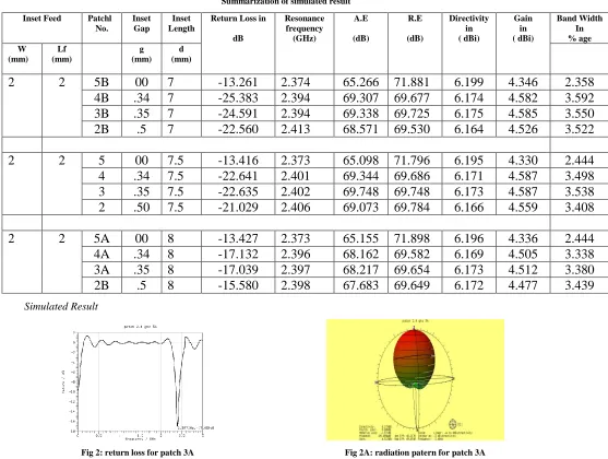
Table 2
Summarization of simulated result
Inset Feed Patchl
No.
Inset Gap
Inset Length
Return Loss in
dB
Resonance frequency (GHz)
A.E
(dB)
R.E
(dB)
Directivity in ( dBi)
Gain in ( dBi)
Band Width In % age W
(mm)
Lf (mm)
g (mm)
d (mm)
2
2
5B
00
7
-13.261
2.374
65.266
71.881
6.199
4.346
2.358
4B
.34
7
-25.383
2.394
69.307
69.677
6.174
4.582
3.592
3B
.35
7
-24.591
2.394
69.338
69.725
6.175
4.585
3.550
2B
.5
7
-22.560
2.413
68.571
69.530
6.164
4.526
3.522
2
2
5
00
7.5
-13.416
2.373
65.098
71.796
6.195
4.330
2.444
4
.34
7.5
-22.641
2.401
69.344
69.686
6.171
4.587
3.498
3
.35
7.5
-22.635
2.402
69.748
69.748
6.173
4.587
3.538
2
.50
7.5
-21.029
2.406
69.073
69.784
6.166
4.559
3.408
2
2
5A
00
8
-13.427
2.373
65.155
71.898
6.196
4.336
2.444
4A
.34
8
-17.132
2.396
68.162
69.582
6.169
4.505
3.338
3A
.35
8
-17.039
2.397
68.217
69.654
6.173
4.512
3.380
2B
.5
8
-15.580
2.398
67.683
69.649
6.172
4.477
3.439
Simulated Result
International Journal of Emerging Technology and Advanced Engineering
Website: www.ijetae.com (ISSN 2250-2459, ISO 9001:2008 Certified Journal, Volume 3, Issue 7, July 2013)
129
Fig 3: return loss for patch 3B Fig 3A: radiation patern for patch 3B
Fig 4: return loss for patch 3 Fig 4A: radiation patern for patch 3
Fig 5: return loss for patch 5 Fig 5A: radiation patern for patch 5
International Journal of Emerging Technology and Advanced Engineering
Website: www.ijetae.com (ISSN 2250-2459, ISO 9001:2008 Certified Journal, Volume 3, Issue 7, July 2013)