165
CHAPTER 9
DELAFOSSITE OXIDE MATERIALS AS A P-TYPE TRANSPARENT CONDUCTING OXIDE
Afishah Alias, Jais Lias, Khairul Anuar Mohamad
Microelectronics and Nanotechnology - Shamsuddin Research Centre (MiNT-SRC), Universiti Tun Hussein Onn Malaysia, Parit Raja, Batu
Pahat, 86400 Johor, Malaysia.
ABSTRACT
Transparent conducting oxides (TCOs) are electrically conductive materials and have been widely utilized in several applications, especially in opto-electrical devices, but TCOs are still used in fabrications of only a few active device. Although most of TCOs are n-type, an increasing number of binary metal oxides with p-type conductivity are also being investigated. For instance, the p-type zinc oxide (ZnO) is difficult to fabricate due to the absence of appropriate dopants. The lithium (Li)-, sodium (Na)-, potassium (K)-, nitrogen (N)-, phosphorus (P)- and arsenic (As)-dopants were observed as deep acceptors, which resulted in no significant p-type conduction of ZnO films. In addition, impurities and lattice defects in ZnO, such as oxygen vacancies and zinc interstitial supply the electrons. A series of TCOs based on copper-based oxide materials such as delafossite copper oxide (CuMO2), where M represents elements in group IIIA, have recently been extensively studied for p-type conductivity materials.
Keywords: Oxide materials, delafossite, transparent conducting oxide (TCO), p-type
9.1 INTRODUCTION
166
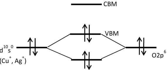
[image:2.420.65.350.250.370.2]in which the upper edge of the valence band is strongly localized to oxide ions [1]. It is known as a single electron pair. When the positive holes are introduced at the edge, charges are then localized on the oxygen ion resulting a deep trap. The positive holes require sufficient amount of energy to cross the large barrier height to migrate inside the crystal lattice, which reduces the conductivity and charge-carrier mobility [2]. A possible solution was proposed where an introduction of a degree of covalency in the bonding of metal-oxygen will induce the formation of an extended valence band structure. This is essential in order to obtain a p-type TCO, and the techniques is called chemical modulation of the valence band (CMVB) [3]. Cationic species are required to serve the CMVB technique, such as the 3d10 closed shell configuration of Cu+ ions and 4d10 closed shell configuration of silver ions (Ag+) [3]. Figure 1 shows a diagram of the CMVB technique. Electron pairs occupy both atomic orbitals and resulting level of anti-bonding is the highest occupied level [2].
Figure 1: Schematic illustration of CMVB technique
According to valence bond theory, the oxide ions are sp3 hybrid orbital in the valence state of an oxygen (O) atom. There are 2s2 orbital in eight electrons in which conveyed on an oxide ion in four σ co-ordination bonds. A nature of non-bonding in oxide ion can be reduced using the electronic configuration and could exhibits a higher quantity of holes at the edge of the valence band. Thus, cuprous oxide (Cu2O) have been recognized as a p-type TCO [4]. However, Cu2O has a narrow band gap in the range of 2.1-2.6 eV [5, 6]. Oxide materials having a delafossite structure of MIMIIIO2 where MI is monovalent ions, such as copper (Cu+) and Ag+ ions and MIII is trivalent ions, such as gallium (Ga+3), aluminum (Al+3), indium (In+3), iron (Fe+3), chromium (Cr+3) and cobalt (Co+3) ions have been formulated to increase in band gap. Each MI atom is facilitated directly with
CBM
VBM
d
10s
0(Cu
+, Ag
+)
O2p
167
two oxygen atoms in order to place an O-MI-O dumbbell unit is parallel with c-axis. All MI layers are linked to the MIIIO2 layers by the O-MI-O dumbbell units. Each oxide ion in the MIIIO2 layer, on the other hand, forms a pseudo-tetrahedral coordination (MIII3MIO) with the neighboring MIII and MI ions [3], thus reduces the nature of non-bonding in the oxide ions and holes are delocalized at the edge of valence band. Moreover, this oxide-layered structure also reduces the cross-linking contribution of MI ions, and thus increases the bandwidth of oxides [1]. This structure also revealed that coordination number of the MI ions is low because of the large separation from oxygen ligands, thus 2p electrons in oxygen ligands and MI d10 electrons form a solid coulombic repulsion. The MI d10 energy levels are being similar to the O 2p level resulted in a high level of mixture. This is important approach to fabricate p-type TCO using CMVB technique [7].
[image:3.420.148.274.361.516.2]The nickel oxide (NiO), as benchmark of oxide materials, have been first discovered as a p-type TCO [8]. Then, there was an improvement over NiO until transparent p-type conductivity films of copper aluminum oxide (CuAlO2) was reported [1]. This result is very promising, although the conductivity was smaller than n-type TCO approximately a factor of 1000. A various p-type TCOs based on Cu+ delafossite oxides were later reported [1, 9-11]. Cu-based TCOs with the delafossite structure have been developed, such as CuMO2 where M is elements in group IIIA including Al, Ga, and In. Figure 2 shows the delafossite oxide crystal structure of CuMO2.
168
9.2 DELAFOSSITE OXIDE
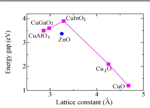
The CuAlO2 is known as a transparent p-type semiconductor material with a direct band gap approximately 3.5 eV. CuAlO2 thin films are synthesized using pulsed laser deposition (PLD) [1,12], plasma enhanced metalorganic chemical vapor deposition (MPE-MO-CVD) [13], DC sputtering [14] and sol-gel [15-18] methods. The carrier concentration, Hall mobility and direct band gap were obtained using pulsed laser deposition method as 2.7 × 1019cm-3, 0.13 cm2/Vs and 3.5 eV, respectively [12]. The CuAlO2 films prepared by laser ablation has obtained the conductivity and carrier concentration about 1 × 10⁻¹ Scm-1 and 1.3 × 1017 cm-3, respectively [1]. The films also exhibit high transparency with 80% of optical transmittance in the visible range. CuAlO2 was also successfully fabricated by a sol-gel method. Precursor materials have been prepared in various ways based on the sol-gel method. For example, the CuAlO2 films was fabricated using copper (II) acetate monohydrate (Cu(CH3COO)2·H2O) and alumatrane as precursor materials [13]. The solution was prepared by continued stirring the mixed solution at the ambient temperatures for 12-hours [15]. Meanwhile, there was a fabrication of CuAlO2 films by nitrate route, where copper and aluminum nitrates were used as precursor materials. The nitrate solution was stirred at the ambient temperatures for 1-hour, followed by additional stirring at 70 oC for 2-hours to obtain jellification [16]. It has been reported previously that the copper indium oxide (CuInO2) has the largest band gap of 3.9 eV. The delafossite CuInO2 shows both p- and n-type conductions using a suitable impurity doping and optimum conditions of the deposition rate. However, the conductivity of CuInO2 films was unfortunately smaller than other p-type TCOs, which reported value of approximately 1 × 10⁻³ Scm−1. In addition, a PLD method was also used to produce a p-type CuInO2 films from phase-pure targets [5].
The discovery of p-type TCOs led to the investigation of transparent semiconductor oxides (TSOs). This indicates the possibility of formation
p-n jup-nctiop-ns usip-ng a combip-natiop-n of TCOs’ p-type and n-type. Figure 3
169
Figure 3: Lattice constant versus energy gap of some p-type materials
9.3 COPPER GALLIUM OXIDE MATERIALS
A CuGaO2 phase is rhombohedral, which belong to the CuMIIIBO2 family. It is known as a good p-type TCO possessing an energy band gap of ~3.6 eV [6]. CuGaO2 has a larger axis lattice constant which is a = 2.98 Å, and comparable to that of CuAlO2 (a = 2.86 Å). The a-axis lattice constant in ZnO is 3.25 Å. Thus, a combination of p-CuGaO2/n-ZnO hetero-layer is progressively ideal for the development of p–n junctions with these delafossite materials in relation to the lattice mismatch. This material configuration has an intermediate electronic structure between CuAlO2 and CuInO2.
170
with the energy band gap of ~3.4 eV was produced for 12-hours in N2 atmospheres by post-annealing at 850 oC. The activation energy at room temperature was approximately estimated at 0.22 eV and the conductivity was approximately 5.6 × 10⁻³ Scm−1 [10].
The challenge in the growth of CuGaO2 films is to minimize the formation of secondary phases, particularly Cu2O and copper gallate spinels (CuGa2O4), which are driven by the variable valence state of the Cu cations [19]. The growth temperature affected the formation of undesirable phases in CuGaO2 films, such as CuGa2O4, gallium oxide (Ga2O3) and CuO, thus indicated it is growth temperature dependence [17]. The films contained CuGa2O4 and CuO at low temperatures below 725 oC, while the phase of Ga2O3 was formed at a higher temperature of 780 oC due to desorption of Cu atoms. Single-phase CuGaO2 films were only obtained at a temperature of around 750 oC which is a narrow growth temperature. The growth temperature dependence of the phase separation of the CuGaO2 thin films was investigated by PLD [18]. The phase is a mixture of CuGaO2, Cu2O and CuGa2O4 at relatively low growth temperatures. Most of the phase at higher temperatures is CuGaO2. The purity of the phase is further improved by annealing at a high temperature. Films with p-type resistivity
of 33.8 Ω-cm, carrier density of 6.3 × 1017 cm-3 and mobility of
approximately 0.32 cm2/Vs were obtained for almost a phase-pure CuGaO2 film.
9.4 SUMMARY
171
REFERENCES
[1] Kawazoe, H., Yasukawa, M., Hyodo, H., Kurita, M., Yanagi, H., & Hosono, H., (1997). P-type electrical conduction in transparent thin films of CuAlO2, Nature, 389, 939-942.
[2] Banerjee, A. N., & Chattopadhyay, K. K., (2005). Recent developments in the emerging field of crystalline p-type transparent conducting oxide thin films, Progress in Crystal Growth and Characterization of Materials, 50(1-3), 52-105.
[3] Kawazoe, H., Yanagi, H., Ueda, K., & Hosono, H., (2000). Transparent p-type conducting oxides: design and fabrication of pn heterojunctions, Materials Research Society Bulletin, 25(8), 28-36.
[4] Zhang, K. H. L., Xi, K., Blamire, M., & Egdell, R. G., (2016). P-type transparent conducting oxides, Journal of Physics Condensed Matter, 28(38), 383002.
[5] Yanagi, H., Hase, T., Ibuki, S., Ueda, K., & Hosono, H., (2001). Bipolarity in electrical conduction of transparent oxide semiconductor CuInO2 with delafossite structure, Applied Physics Letters, 78(11), 1583.
[6] Ueda, K., Hase, T., Yanagi, H., Kawazoe, H., Hosono, H., Ohta, H., Orita, M., & Hirano M., (2001). Epitaxial growth of transparent p-type conducting CuGaO2 thin films on sapphire (001) substrates by pulsed laser deposition, Journal of Applied Physics, 89(3), 1790.
[7] Yanagi, H., Kawazoe, H., Kudo, A., Yasukawa, M., & Hosono, H., (2000). Chemical design and thin film preparation of p-type conductive transparent oxides, Journal of Electroceramics, 4(2-3), 407-414.
[8] Sato, H., Minami, T., Takata, S., & Yamada, T., (1993). Transparent conducting p-type NiO thin films prepared by magnetron sputtering. Thin Solid Films, 236(1-2), 27-31.
[9] Kudo, A., Yanagi, H., Hosono, H., & Kawazoe, H., (1998). SrCu2O2: a p-type conductive oxide with wide band gap, Applied Physics Letters, 73(2), 220.
172
Hamada, N., (2000). Electronic structure and optoelectronic properties of transparent p-type conducting CuAlO2, Journal of Applied Physics, 88(7), 4159.
[11] Gong, H., & Wang, Y., (2000). Nanocrystalline p-type transparent Cu–Al–O semiconductor prepared by chemical-vapor deposition with Cu(acac)2 and Al(acac)3 precursors, Applied Physics Letters, 76(26), 3959.
[12] Banerjee, A. N., Kundoo, S., & Chattopadhyay, K. K., (2003). Synthesis and characterization for p-type transparent conducting CuAlO2 thin film by dc sputtering, Thin Solid Films, 440(1-2), 5-10.
[13] Gotzendorfer, S., Polenzky, C., Ulrich. S., & Lobman, P., (2009). Preparation of CuAlO2 and CuCrO2 thin films by sol-gel processing, Thin Solid Films, 518(4), 1153-1156.
[14] Ghosh, C. K., Popuri, S. R., Mahesh, T. U., & Chattopadhyay, K. K., (2009). Preparation of nanocrystalline CuAlO2 through sol–gel route,
Journal of Sol-Gel Science and Technology, 52(1), 75-81.
[15] Ding, J., Sui, Y., Fu, W., Yang, H., Liu, S., Zeng, Y., Zhao, W., Sun, P., Guo, J., Chen, H., & Li, M., (2010). Synthesis and photoelectric characterization of delafossite conducting oxides CuAlO2 laminar crystal thin films via sol–gel method, Applied Surface Science, 256(21), 6441-6446.
[16] Tonooka, K., Shimokawa, K., & Nishimura, O., (2002). Properties of copper–aluminum oxide films prepared by solution methods, Thin Solid Films, 411(1), 129-133.
[17] Mine, T., Yanagi, H., Nomura, K., Kamiya, T., Hirano, M., & Hosono, H., (2008). Control of carrier concentration and surface flattening of CuGaO2 epitaxial films for a p-channel transparent transistor, Thin Solid Films, 516(17), 5790-5794.
[18] Varadarajan, V., & Norton, D. P., (2006). CuGaO2 thin film synthesis using hydrogen-assisted pulsed laser deposition, Appied Physics A, 85(2), 117-120.
173
CHAPTER 10
THEFAILUREOFINTEGRATEDCIRCUIT:TESTAND ANALYSIS
Hasliza Hassan
Faculty of Electrical and Electronic Engineering,
Universiti Tun Hussein Onn Malaysia, 86400 Parit Raja, Batu Pahat, Johor, Malaysia.
ABSTRACT
Failure analysis (FA) is an important function in the development and manufacturing of integrated circuits. It provides essential information for troubleshooting a complex device while ensuring reliability of a product. The objective of FA is to identify cause of failure and initiate corrective actions. Complex engineering knowledge is required in understanding the nature of a device failure, identifying the problem and subsequently providing a solution to avoid the failure again during the production of the device. FA identifies the causes of failure by analyzing stresses and other mechanisms causing failure. Device failure is defined as any non-conformance of the device to its electrical and/or visual/mechanical specifications. A failure mechanism usually leads to an identifiable change in a device. This chapter reveals the common techniques in troubleshooting IC and flow for identifying FA which consists of fault localization, de-processing, defect localization and inspection characterization. A failed component can provide important information to enhance the reliability of a device or product.
Keywords: failure analysis, troubleshooting, fault localization, reliability
10.1 INTRODUCTION
174
manufacturing practice to reduce and minimize the number of defects and errors in a process and to do things right at the first time. The ultimate aim is to reduce the number of defected products to zero. However, zero-defect means zero failures during operation but not necessarily implies zero imperfections, blemishes, or nonconformities [2].
Failure Analysis (FA) is the process of determining the physical root cause of component failure, troubleshooting a device, where determining how or why a semiconductor device has failed. Failure analysis is necessary in order to understand what caused the failure and how it can be prevented in the future. Device failure is defined as any non-conformance of the device to its electrical and/or visual/mechanical specifications. Therefore, destructive and non-destructive methods involved during the analysis process. Sometimes non-destructive analysis can turn into destructive analysis due to improper handling and incorrect technique performed on the sample.
10.2 Failure Analysis Terminology
[image:10.420.81.357.370.485.2]Some terminology associated with failure analysis will be introduced. These terms are commonly used in written report and communications between the failure analysis department and the customers. The customer plays the key role in specifying the specifications of a device explicitly. The terms are as presented in Table 1.
Table 1: Terminology used in failure analysis
Failure
Description Statement that explains on device failure; normally how much the device deviating from the specifications stated.
Failure
Mechanism Detailed description on the anomalies behind the failure of a device.
Root Cause Cause or factor a nonconformance and the
fundamental reason for the occurrence of a problem.
Fault
175
10.3 FAILURE ANALYSIS PROCESS FLOW
Failure analysis starts with failure verification. Failures can occur during
several points of a product’s life cycle and during manufacturing. It is
important to validate the failure of a sample prior to failure analysis in order to conserve valuable FA resources. Failure verification is usually performed to characterize the failure mode. Moreover, good characterization of the failure mode is necessary to make the FA efficient and accurate.
After failure verification, the failure analysis engineer subjects the sample to various FA techniques step by step, collecting attributes and other observations along the way. Attributes is referred to properties, characteristics and functionality of the samples in order to find the root cause of the failure. Failure analysis start with non-destructive analysis and if necessary destructive analysis will be performed subsequently. The results of various steps must be corroborative and consistent. Any inconsistency in results must be evaluated before proceeding to the next FA step. The most important factor in failure analysis is how far the failure location can be narrowed down while still maintaining the failure symptoms (undestroyed state).
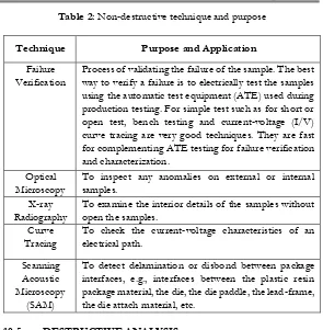
10.4 NON-DESTRUCTIVE ANALYSIS
176
Figure 1: The basic failure analysis flow
In order to understand the failure from customer’s, verifications step are
177
Table 2: Non-destructive technique and purpose
Technique Purpose and Application
Failure Verification
Process of validating the failure of the sample. The best way to verify a failure is to electrically test the samples using the automatic test equipment (ATE) used during production testing. For simple test such as for short or open test, bench testing and current-voltage (I/V) curve tracing are very good techniques. They are fast for complementing ATE testing for failure verification and characterization.
Optical Microscopy
To inspect any anomalies on external or internal samples.
X-ray Radiography
To examine the interior details of the samples without open the samples.
Curve Tracing
To check the current-voltage characteristics of an electrical path.
Scanning Acoustic Microscopy
(SAM)
To detect delamination or disbond between package interfaces, e.g., interfaces between the plastic resin package material, the die, the die paddle, the lead-frame, the die attach material, etc.
10.5 DESTRUCTIVE ANALYSIS
After a failure is confirmed (during non-destructive), the next part is localized the area of failure. In this step, normally the will open for visual inspection and other steps in the internal package. In destructive techniques, the samples will change and alter permanently either by using chemical, mechanical or electrical methods [4-5]. Table 3 list steps that call as destructive techniques and the applications.
10.6 FAULT LOCALIZATION
178
complexity of an electronic devices challenging factors to accurately localize faults prior to any destructive FA tests. Normally, destructive technique such as photon emission microscopy (PEM), fluorescent micro-thermal imaging and liquid crystal hot spot analysis are used to localize the failure areas [7].
These tools are expensive and require experienced personnel trained in integrated circuit (IC) layout, testing and the technique itself in order to optimize the testing processes. Both of physical and electrical steps are required to identify and localize the failure. In modern devices, fault localization step is more challenging due to complexity of the package and complexity of the systems in the devices increased sharply. The complexity is defined as the total number of transistors and the total wiring length on the IC.
Table 3: Destructive test techniques and applications
Technique Application
Decapsulation A process for opening the IC package before visual inspection, chemical analysis, or electrical examination of the die and the internal features of the package. For hermatic package, the process is referred to as 'delidding' or 'decapping.'
Cross Sectioning
A technique for mechanically exposing a plane of interest in a die or package for further analysis or inspection. Normally, this consists of sawing, grinding, polishing, and staining the specimen until the plane of interest is ready for optical or electron microscopy
Hot Spot Detection/ Liquid Crystal
To locate areas on the die surface that exhibit excessive heating. Excessive heating indicates a high current flow, which may be due to die defects or abnormalities like dielectric ruptures, metallization shorts, and leaky junctions.
Light Emitting
179
Microprobing To achieve electrical contact with or access to a point in the active circuitry of the die. Electrical contact is made by dropping fine-tipped probe needles directly on the point of interest, or on an area to which the point of interest is connected.
Scanning Electron Microscope
(SEM)
For inspecting topographies of specimens at very high magnifications with real-time imaging.
Energy Dispersive
X-ray (EDX)
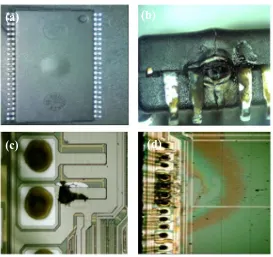
[image:15.420.81.354.234.491.2]For identifying the elemental composition of the specimen, or an area of interest.
Figure 2: Electrical over-stress phenomena. (a) Bulging of package, (b) Burnt or crack package, (c) Burnt Metal and (d) heat stressed silicon.
(a)
(b)
180
10.7 ROOT CAUSES IN IC FAILURES
After localizing the area of failure in an integrated circuit, failure analysis engineer will find the cause of the failure. Anomalies in the function of the sample is caused by the change of resistance in between any electrical nodes or in any electrical path of the samples. However, the samples normally do not fail for electrical reasons but caused by either physical, chemical, or mechanical faults.
The two main classifications of failures are overstress and wear-out. Overstress is a condition where extreme conditions were applied exceeding the strength of materials. The condition occurs abruptly, and it is catastrophic [8]. Wear-out is an accumulation of damage under extended usage or repeated stress applications. Wear-out and overstress test can be detected as early during reliability test.
The major failures are due to electrical overstress (EOS) and electrostatic static discharge damage (ESD). EOS phenomena are the thermal damage that occur when the device is subjected to a voltage and current that induced heat which is over the specified heat limits of the device [9-10]. Heat generated during EOS event result of resistive heating and localized high temperatures in the devices. Some examples are as shown in Figure 2. The high temperature causes destructive damage to the materials used in the
device’s construction.
Electrostatic Discharge (ESD) is a phenomenon when abrupt current flows between two electrically charged objects caused by contacts, an electrical short, or dielectric breakdown. ESD can create electric sparks and causes two main failures. First failure is associated with the danger of gate oxide dielectric breakdown due to the high voltage seen during ESD events in a CMOS device [11]. The thin gates of an input buffer are tied directly to the input pin and thus, are especially vulnerable to oxide breakdown. Dielectric breakdown is also of concern within the protection circuits since thin-gate MOS devices are commonly used.
181
10.8 SUMMARY
This chapter summarizes general steps in failure analysis. Failure analysis and investigation are to determine the root cause of failure the devices, component or asset fail or not perform as expected. The findings from failure analysis will be used to take remedial action and prevent from recurrence.
REFERENCES
[1] Golagha, M., Pretschner, A., Fisch, D. and Nagy, R. (2017). Reducing failure analysis time: An industrial evaluation. 2017IEEE/ACM 39th International Conference on Software Engineering: Software Engineering in Practice Track (ICSE-SEIP), 293-302.
[2] Calvin, T. (1983). Quality control techniques for zero defects. IEEE Transactions on Components, Hybrids, and Manufacturing Technology, 6(3), 323-328.
[3] Kim, H., Um, K.H. and Shin, S.J. (2008). Failure analysis of Integrated circuits based on nondestructive evaluation. In Advanced Nondestructive Evaluation II: Volume 2, 1364-1369.
[4] Tsai, N.S., Rana, V.V.S., Huttemann, R.D., Wong, Y.M., Haynes, R.W., Singh, R. and Manocha, A.S. (1988). December. Layer tungsten and its applications for VLSI interconnects. Technical Digest, International Electron Devices Meeting, 462-465.
[5] Chim, W.K. (2000). Semiconductor device and failure analysis: using photon emission microscopy. Wiley.
[6] Wagner, L.C. ed. (1999). Failure analysis of integrated circuits: tools and techniques (Vol. 494). Springer Science & Business Media.
[7] Muchaidze, G., Koo, J., Cai, Q., Li, T., Han, L., Martwick, A., Wang, K., Min, J., Drewniak, J.L. and Pommerenke, D. (2008). Susceptibility scanning as a failure analysis tool for system-level electrostatic discharge (ESD) problems. IEEE Transactions on Electromagnetic Compatibility, 50(2), 268-276.
182
solution [CMOS], Physical and Failure Analysis of Integrated Circuits,
Proceedings of the 9th International Symposium on the IPFA 2002.
[9] Ruan, J., Papaioannou, G.J., Nolhier, N., Mauran, N., Bafleur, M., Coccetti, F. and Plana, R., (2008). ESD failure signature in capacitive RF MEMS switches. Microelectronics reliability, 48(8-9), 1237-1240.