2017 International Conference on Computer, Electronics and Communication Engineering (CECE 2017) ISBN: 978-1-60595-476-9
A Hardware Design of High-throughput and Resource-saving
Image Convolution
Lei-zhi SHU
*, Yuan-xi PENG, Zhe CHEN and Xing-yu NIE
State Key Laboratory of High Performance Computing, National University of Defense and Technology, Changsha, China
*Corresponding author
Keywords: Image convolution, Shifting register chain, Data multiplex, Logic duplication.
Abstract. This paper proposes a hardware design of high-throughput and resource-saving image convolution. The key part of the design is consist of two aspects, buffer and computing part. For the buffer part, serial shifting register chain has been applied to buffer some of the pixels so that large number of buffer resources could be saved, thus realizing data multiplex; as for computing part, logic resource consumed is not much but time consumed for the serial convolution operation is too long. Since buffer part consumes little resource, logic duplication can be used to realize parallel design, thus accelerating the convolution operation, which reduces the time consumed largely and makes the throughput higher. In one word, this design not only accelerates the convolution operation, but also reduces the consumed resources.
Introduction
Background Introduction
Artificial neural network is a computer vision model inspired by the biological visual neural network. It designs the multi-layer neuron model by imitating the biological (human) brain which recognizes objects by vision, so that the computer vision recognition system can improve recognition rate, and achieve strong resistance to displacement and deformation interference [1]. The convolution
neural network [2] algorithm is a new algorithm of computer vision field. On the basis of traditional
neural network, the number of parameters is reduced by weight sharing, local interconnection, down-sampling, multi-layer convolution, and so on, and then direct image input, feature extraction, objects classification, recognition etc could all be implemented. In the field of image recognition, convolution neural network can achieve high recognition rate, and can overcome the image displacement and deformation [3].
Since the convolutional neural network is a computationally intensive algorithm, and its operation mainly consists of a large number of independent repetitive multiplication and addition operations. It will cost large amount of time if these repetitive multiplication and addition operations run on CPU, therefore, it is increasingly necessary to parallelize the algorithms, thus speeding up the programs.
The Principle of Image Convolution
Based on single image frame, the mathematical model of CNN is deduced as followed by analyzing the features of single image frame while performing convolutional operation according to the convolution theorem of digital image. Suppose the convolution kernel size is N * N, each pixel is represented in a binary 9-bit integer, the mathematical model of image convolution is as follows:
N i N j N j y N i x j i y x a o1 1 2
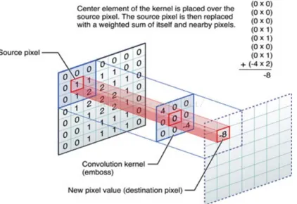
[image:2.612.202.413.247.392.2]1 , 2 1 , , (1) According to the above model, detailed description is as follows. When the convolution kernel is placed in the upper left corner of the image, the convolution template will coincide with the N * N segmentation matrix in the upper left corner of the image. Multiply their corresponding items and then add them all to get the first element of the feature map, as shown in Figure 1.
Figure 1. The principle of single channel image.
Then move the convolution kernel to right by one step, and then the next point of the feature map can be calculated. In this way, the whole feature map will be achieved while the convolution kernel traverses the whole image.
When the image has more than one channel and the number of convolution kernel is over one, the specific math model of image convolution is as follows:
1 0 1 0 1 0 ))) * , * , ( * ) , , , ( ( ( ) , , ( xn m kh v kw u sh j v sw i u m x v u m n w j i n o (2) In formula (2), kw represents the width of a convolution kernel, and kh represents the height of aconvolution kernel, while sw represents the horizontal step when the kernel traverses the image. And sh represents the vertical step. xn represents the number of the input image channels, and o(n,i,j)
represents the pixel value in the position (i,j) of the nth channel of the output feature maps. While
x(m,i,j) represents the pixel value in the position(i,j) of the mth channel of the input images, and
w(n,m,u,v) represents the weight, n represents the nth channel of the output feature maps and m
represents the mth channel of the input image. u and v represents particular position of the kernel.
Different kernel doing convolution operation with the image will obtain different feature map of the image, therefore, the number of the output feature maps is equal to the number of convolution kernels. As figure 2 shows, six kernels achieve six feature maps.
The Scheme of Hardware Design of Image Convolution
Figure 2. Image convolution principle for multi kernels.
As the area of alan’s design is too big, and the performance is not so good. To achieve a relative excellent implementation, our scheme is proposed. It has two innovations. The first one is reuse of buffer logics, namely, using shift registers chain to buffer the input image pixels, which has saved lots of time and resources compared to alan’s scheme. The second one is called logic duplication, namely, for the multi-kernel convolution, more than one data path have been applied to realize parallelism, thus accelerating the convolution speed.
Introduction To The Overall Architecture
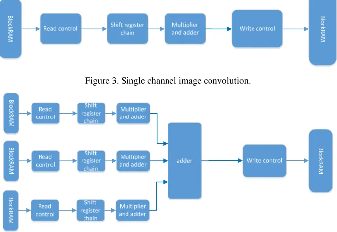
[image:3.612.136.477.404.639.2]As figure 3 shows, the proposed scheme for single channel image consists of three basic parts, namely, shift register chain, multiply and accumulation module and the control module. However, the design as figure 3 shows can only realize image convolution for one channel, to accomplish multi-channel convolution, such as three channels image, multiple data path should be integrated in a design, thus realizing parallelism for the operation. As figure 4 shows, architecture of three channels image convolution has been proposed.
Figure 3. Single channel image convolution.
Figure 4. Architecture of three channels image convolution.
Shift Registers Chain
[image:4.612.191.421.132.297.2]In the proposed scheme, the size of convolution kernel is 7 * 7, and the size of the input image is 150 * 150. So the shift register chain in the design consists of 7 * 150 registers. Pixels of the input image flow along the shift register chain one by one, as figure 5 shows.
Figure 5. Shift register chain.
Pixels will be fetched out while the address of blockRAM adds 1 in every circle. And then these pixels will be put into the shift register chain. Suppose the position of the first register is (0,0) , when pixels move from the (0,0) position to the (6,149)position, it will get abandoned. When the first pixel moves to the register at (6,6) as it shows in the dashed box in figure 5, it equals that the convolution kernel coincide with the 7 * 7 segmentation matrix in the upper left corner of the input image. And then the kernel will do convolution operation with the matrix of the dashed box, thus getting the first element of the feature map.
After that, all the data in the shift register chain move by one step as the clock passes by one cycle, and the data in the dashed box updates, too. As time passes by, all the pixels in the input image will flow through the shift register chain. In this manner, reuse of buffer logic is implemented. Compared to alan’s [7]project, the proposed scheme has saved lots of buffer resources.
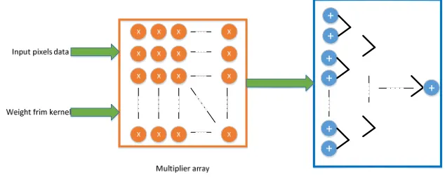
Multiplication and Accumulation Module
The multiplication and accumulation module is the key module of the overall scheme, which accomplish the convolution operation, and obtain the final feature maps. This module consists of two parts, namely, multiplier array and adder tree, as is showed in Figure 6.
[image:4.612.152.469.530.663.2]The Control Module
In the control module, pixels are fetched from the BlockRAM0 (storing image) and sent to shift register chain, while the results of adder tree are sent to BlockRAM1(storing feature maps). This module mainly focuses on enable signals, addresses for those BlockRAMs, and some other control signals.
Experiments
Simulation Result
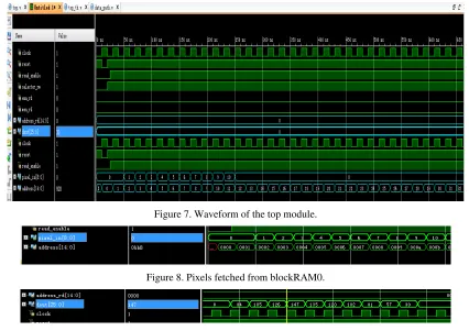
[image:5.612.92.518.268.569.2]Since 7 instantiations of the circuit in Figure 4 are the same, experiments are focused on the circuit in Figure 4. The frequency of the clock is set to 250MHz, and the first ten pixels of the input image are set to 1, 2, 3, 4, 5, 6, 7, 8, 9, 10; then the rest pixels of the image are all set to 0. The first ten elements of the convolution kernel are all set to 1, the rest are all set to 0. The simulation results are depicted in the following.
Figure 7. Waveform of the top module.
Figure 8. Pixels fetched from blockRAM0.
Figure 9. Elements of feature map written to blockRAM1.
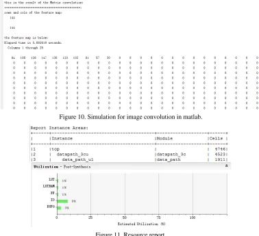
Experiments have been conducted both in vivado and in matlab. The input data and weights of kernel are the same in two simulators. And the results in both platforms are the same as is shown in Figure9 and Figure 10. Therefore, the logic function of the proposed design is correct.
Result of Synthesis and Implementation
Figure 10. Simulation for image convolution in matlab.
Figure 11. Resource report.
As depicted in Figure 11, the LUT , LUTRAM and FF resource utilized by the proposed design are all 1%, and IO resource utilized is 8%, while BUFG resource utilized is 3%. As the FPGA chip is xc7vx485tffg1157, the specific resource utilization is as depicted in table 1.
Table 1. FPGA resource utilization.
LUT[number] LUTRAM[bit] FF[number] IO[number] BUFG[bit]
Proposed circuit 4746 680k bit 4746 96 245.25k bit
Alan’s >485760 4760k bit —— —— ——
All of FPGA 485760 37080k bit 485760 1200 8175k bit
[image:6.612.98.521.598.635.2]Considering the 7 instantiations of the circuit in Figure 4, some key technical indicators of the overall circuit are shown in Table 2. By contrast, the throughput of the proposed design is more than twice of alan’s while resources utilized by alan’s are far more than the proposed scheme.
Table 2. Key indicators of the overall scheme.
indicators throughput[MAC/s] BlockRAM[Byte] BUFFER[number]
Alan’s 100 G 694.8585 k 472500
proposed 257.25 G 694.8585 k 22050
Conclusion
References
[1] J. Li and L. Yu, "Using BP nerual networks for the simulation of energy consumption," 2014 IEEE International Conference on Systems, Man, and Cybernetics (SMC), San Diego, CA, 2014, pp. 3542-3547.
[2] G. Cheng; Y. Wang; S. Xu; H. Wang; S. Xiang; C. Pan, "Automatic Road Detection and Centerline Extraction via Cascaded End-to-End Convolutional Neural Network," in IEEE Transactions on Geoscience and Remote Sensing, vol. PP, no.99, pp. 1-16.
[3] Xie Baojian. Study on image classification method based on convolution neural network [D]. Hefei University of Technology, 2015.
[4] Qi Liu, Zi Huang and Fuqiao Hu, "Accelerating convolution-based detection model on GPU," 2015 International Conference on Estimation, Detection and Information Fusion (ICEDIF), Harbin, 2015, pp. 61-66.
[5] Zhu Xueliang, Chai Zhilei, Zhong Chuanjie, Zhang Ping. Design and Implementation of Image Convolutional IP Core Based on FPGA [J]. Microelectronics and Computer, 2011, (06): 188-192 [J]. [6] Sang Hongshi, Liao Dingbin, Jiang Wei. Implementation of a new 2-D convolution on FPGA. [J]. Microelectronics and Computer, 2011, (09): 27-30.
[7] Information on https://github.com/alan4186/Hardware-CNN.
[8] S. Di Carlo, G. Gambardella, M. Indaco, D. Rolfo, G. Tiotto and P. Prinetto, "An area-efficient 2-D convolution implementation on FPGA for space applications," 2011 IEEE 6th International Design and Test Workshop (IDT), Beirut, 2011, pp. 88-92.