Efficient Router Architecture Design on FPGA for Torus
based Network on Chip
Saraswathi Venugopal
A.R.J College of Engineering and Technology, Mannargudi
Tamilnadu, India.
Arokiasamy
Arulanandasamy
A.R.J College of Engineering and Technology Mannargudi Tamilnadu, India.
R. Ramachandran
Research scholar, Manonmaniam Sundaranar University Tamilnadu,IndiaABSTRACT
Network-on-Chip (NoC) is an emerging technology for interconnecting multiple cores on a single silicon chip. In NoCs, hardware modules such as CPU cores, memories and I/O controllers are interconnected through a suitable network topology for sharing the data. This paper proposes a Multiprocessor NoC (MPNOC) based on torus network topology using wormhole switching. This NoC architecture consists of heterogeneous processing elements and core interfacing devices. We show that the proposed novel router architecture composed of small crossbar switch with Virtual channel memory requires less logical resources and reduce the routing complexity in wormhole switching in torus which provide high throughput performance evaluation and FPGA implementation of the system results are also given.
Keywords
NoC, Router design, SoC, FPGA, Network on Chip.
1.
INTRODUCTION
Revolution of Deep Sub-Micron (DSM) technology has shrunk the size of transistor and increased the number of transistors on a silicon chip, allowing the design and integration of large number of processing cores and memory on a single chip. These processing cores can be a CPU or digital signal processors and I/O controller, memory interface controller [1]. System-on-chip (SoC) is a system, consisting of a processing core as well as analog and digital circuits built on a single silicon chip. The circuits and the processor are interconnected by means of buses [2]. While, the number of processors on a SoC is increased, bus arbitration and bandwidth became the bottleneck. The architecture encountered physical limitations such as delay and power due to long wires, and parasitic capacitance [3]. Network on Chip (NoC) has been proposed as an emerging paradigm for interconnecting multiple processing cores on a single chip. The NoC employs a layered architecture and uses network topology for interconnecting and sharing the data between the components on the chip. It is an efficient alternative to traditional dedicated wires for achieving high performance, modularity and overcoming the bottlenecks in the communication infrastructure of SoC[4][5][6][7][8].
In the design of NoC, the areas must be concentrated are switching, packet communication between nodes, and network topologies. There are two types switching methods in the design of NoC, known as packet switching and circuit switching. Circuit-switching forms a path from source to destination prior to transfer by reserving the routers (switches)
path is turned down after the transfer has completed. Packet-switching is more common and it is utilized about 80% of the design of NoCs. Some sources assume packet-switching as key property of NoCs. There are three techniques of how packets are forwarded and stored at routers: 1. store-and-forward, 2. cut-through, and 3. wormhole, Store-and-forward (s) method waits for the whole data packet before making routing decisions whereas cut-through (c) forwards the packet already when the header information is available. Both methods need buffering capacity for one full packet at minimum. Wormhole switching (w) technique is popular and well suited on chip. In this switching, the data packets are split into several flits (flow control digits), and then routing is done as soon as possible. As for topologies concerned, most common topologies are 2-D mesh and torus which constitute over 60% of cases. Both have connections between 4 neighbour nodes but torus has wraparound links connecting the nodes on network edges and mesh does not [9][10].
Field Programmable Gate Array (FPGA) is a good platform for implementing NOC framework and developing a SoC prototype. It provides some basic building blocks such us soft core CPU, peripheral interface controller, on-chip memory and phase lock loop required for implementing NoC [11][12].
The proposed NoC framework is constructed using torus topology [12] and uses the wormhole switching for data communication. The router architecture consists of multichannel crossbar switch and virtual channel for increasing the throughput. This paper is organized as follows. Section 2 describes the structure and functionality of the proposed NOC work. The section 3 provides the synthesized results of proposed system and section 4 provides the conclusion of our work.
2.
FUNCTIONALITY AND STRUCTURE
OF THE NOC TYPESET TEXT.
Volume 55– No.14, October 2012
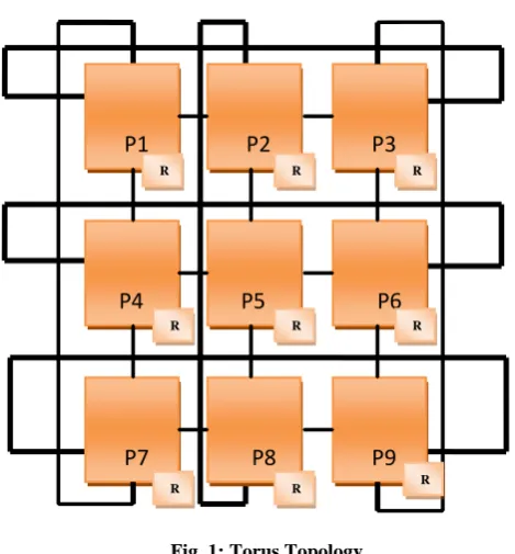
Fig. 1: Torus Topology
2.1
Master & Slave processing units
The master processing unit consists of NIOS II soft core processor; it’s a general purpose 32-bit Reduced Instruction Set Computer (RISC) processor core based on Harvard memory architecture. It consists of 32 general-purpose registers, it has Single-instruction for 32x32 multiply and divide operations, and dedicated instructions for 64-bit and 128-bit products of multiplication. The slave processing unit consists of UART, TIMER, and Instruction/Data Memory, memory interface controllers such as SRAM, SDRAM, and Dual SDRAM.
2.2
Network interface
Master and slave processing unit’s connected to the Communication Infrastructure through a Network Interface (NI). It's shown in fig 2. It receives signals from PUs and generates packets to be sent to the router module. The main function of the Network Interface module is to convert the data to and from the format required by core Infrastructure. The soft core processor enabled a data transfer to and from a slave unit as well as to different reconfigurable hardware blocks. SPU responds to the requests from master command either by sending back the requested signals/data or by saving the received information. NI is executing as a Moore Machine shown in fig. 3 which is triggered by the control signals generated from the PE and generates the packet.
[image:2.595.317.547.73.566.2]Fig. 2: Block Diagram of NI
Fig. 3: State Diagram of NI
2.3
Router
In the design of NOC framework torus topology is used as it is simple and effective shown in figure 4. In this topology, each node has individual router having 5 inputs and 5 outputs. This router architecture designed with three 3×3 smaller crossbar switches with virtual channel flow control shown in fig 5 instead of single 5x5. The major advantage of this design with virtual channel flow control reduces routing complexity in wormhole switching and consumes less number of buffers.
.
Initial state
Read Request from PU/Router
Process the packet Forward to
PU/Router wait for ACK
P1
P2
P3
P4
P5
P6
P7
P8
P9
R 1 R 1
R 1
R 1
R 1
R 1
R 1 R 1
R 1
I/O Buffer
FSM Based control Unit
Register Array
Processing
Fig.4: Block Diagram of Router
Fig. 5: Crossbar switch
In this technique, the information packets from North/ South (Versa) router’s outputs are routed via crossbar switch ONE and East/West (Vice versa) router’s outputs are routed via crossbar switch two. In case, packets to be transferred in the alternative direction (i.e. East/North or for the West/South or Vice versa) router outputs the Packets through third cross bar switch called PU crossbar switch. In case PU wants to communicate with any one of the directions (East West -North - South) it transfers the packet to PU crossbar switch. This smaller crossbar switch technique increases the utilization of the output channels to obtain a high network throughput. The control logic of the routing unit is a finite state machine (FSM). It processes the packet header to compute an appropriate output channel and generates requests for that output channel accordingly. Moreover, the routing unit provides the handshaking response signals (ACK or NACK) to the sender in order to indicate packet acceptance status.
2.4 Virtual channels
Virtual channel flow control allows minimization of the size of the router’s buffers a significant source of area and energy overhead while providing flexibility and better channel utilization. This configurable router employs a modest number of virtual channels to improve network throughput and reduce the effect of blocking. The virtual channels are
are implemented with separate buffers for each virtual channel. The configurable router with virtual channel support provides two logical links per physical channel. Each pair of virtual channels is multiplexed to each of the physical channels provided by the dual-crossbar organization. A dedicated controller orchestrates the data multiplexing of the virtual channels onto the physical channel.
3.
SIMULATION
AND
FPGA
IMPLEMENTATION RESULTS
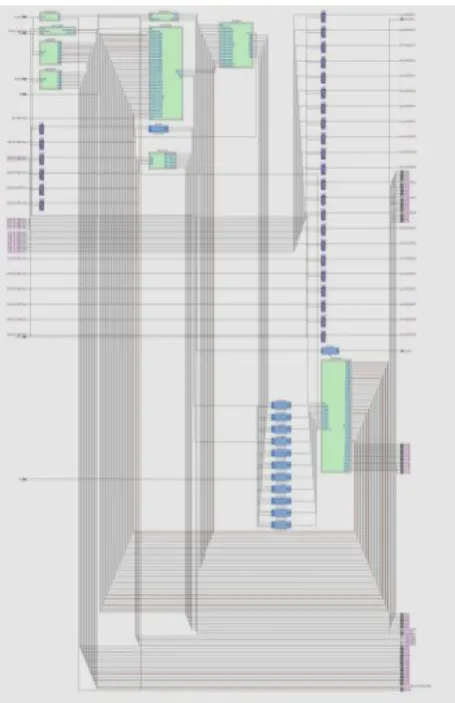
The NOC system consists of NIOS II soft core processor, VGA controller, I2c controller, PS/2 keyboard controller, UART controller, SRAM controller and SDRAM controller. The proposed system was designed using ALTERA CAD tools and tested on ALTERA DE2 70 Development board. In the design, the SOPC Builder component editor is used to configure the node element NIOS II soft processor using Altera’s standard components and a custom network interface component created for this work. Software development for the NIOS II soft processor in the node element is done using the NIOS II IDE. Altera Quartus II is the FPGA implementation tool used to compile the final NOC system design. It generates the resulting configuration bit stream. The figure (6) shows RTL view and timing analyser of the main components.
Fig. 6: RTL view of NoC Frame work South
In/Out In/Out
East In/Out West
In/Out
Left/Right PU
E/w
N/S PU
Left/Rig ht
Left
P U
Right
U
[image:3.595.317.545.365.717.2]Volume 55– No.14, October 2012
Processing Element Utilized logic
NIOS II Soft-core Processor 1498
Router architecture 246
Core interface 188
UART 196
Timer 35
I2C controller 95
SRAM controller 432
SDRAM Controller 105
VGA Controller 348
Table 1: Logic Utilization
[image:4.595.53.265.69.310.2]Table 1 is the illustration of number of logic utilization of different modules in the WH, with 4 Virtual Channels based NOC design. The floor planning output is shown in figure 7.
Fig 7: Floor planning output
In order to evaluate system performance it is tested with the program, which continuously generates the task from NIOS II CPU and forward to slave modules UART and PS/2 keyboard controller, SRAM controller and I2C controller. The response of these modules was studied with help of logic analyzer. The 50 MHz clock was used for the functioning of master processing unit and 100 MHz to NOC network and Slave PEs include a TIMER, UART, and normal Data Memory unit working at 27MHz.
Module Number of bits Per packet
Virtual channel Buffer size
Traffic
UART 10bits 1kbyte Medium
SRAM Controller
35 bits 128 byte Low
PS/2
Controller
12 bits 128 byte Low
I2C controller
18 bit 512 byte Low
Table 2. Traffic of Processing elements
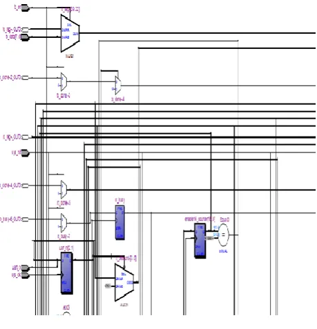
The table 2 illustrates the studies, which reveals that UART needs large virtual channel buffer over other PEs, because most of UART based interface device is working with 9600 baud rate (9.6Kbyte). It creates more traffic than other PEs in the network. In order to reduce the traffic in the network, there is a need of increase in the virtual channel buffer in UART router. RTL view of the UART controller is shown in figure 8.
Figure 8. RTL View of UART Controller
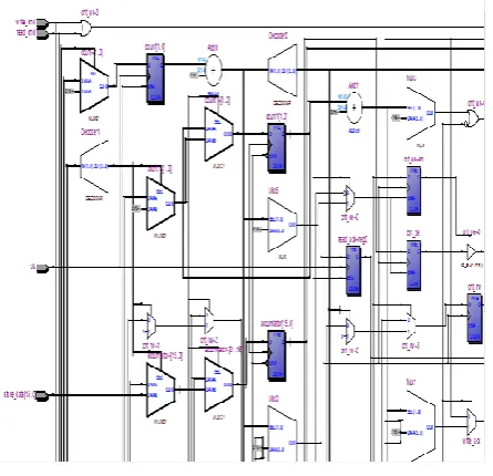
[image:4.595.55.265.391.608.2] [image:4.595.319.549.402.641.2]Figure 9 illustrates the RTL view of SRAM Controller. Also figure 10 and 11 represents the RTL view of the PS/2 keyboard controller and I2C controller respectively.
[image:5.595.319.528.153.253.2]Figure 9. RTL View of SRAM Controller
Fig 10. RTL view of PS/2 keyboard controller
Figure 11. RTL View I2C controller
I2C controller is working in basic system whose operating speed is from 10 to 100 kHz. Its require less number of virtual channel buffer compared to serial controller.
The timing wave form in Figure 12 shows that the processing time of Network interface to each packet came from router or processing unit.
Figure 12. Processing Timing diagram of Network Interface
4.
CONCLUSION
Synthesizable Multiprocessor NOC architecture has been implemented in programmable logic with torus topology and wormhole switching. This system is implemented using a tool chain that is comprised of commercial Altera software and custom high-level system specification software. The newly introduced method of 3x3 crossbar switch based router architecture has proven better latency compared to normal worm hole with single cross bar switch. It offers higher performance and is more area efficient. A processing element consisting of a pipelined NIOS II processor, on-chip memory, external interface, and a network interface is associated with each configurable router. FSM- based network interface also improves processing element performance because it carries out the packet and unpacked function. The synthesis results have demonstrated better resource utilization.
5.
REFERENCES
[1] Constantinescu et al "Impact of Deep Submicron Technology on Dependability of VLSI Circuits",DSN '02 Proceedings of the 2002 International Conference on Dependable Systems and Networks.
[2] SuganyaK. ,Nagarajan, V. "Efficient run-time task allocation in reconfigurable multiprocessor System-on-Chip with Network-on-System-on-Chip",Computer, Communication and Electrical Technology (ICCCET), 2011 International Conference DOI : 10.1109/ICCCET.2011.5762458.
[3] William J. Dally and Brian Towles,"Route Packets, Not Wires: On-Chip Interconnection Networks", 2001 ACM 1-58113-297-2/01/0006.
[4] YiboXue et al, "Network caching for Chip Multiprocessors”, Performance Computing and Communications Conference (IPCCC), 2009 IEEE 28th International.
[image:5.595.71.284.377.539.2]Volume 55– No.14, October 2012
[6] Boris Grot et al, “Kilo-NOC: A Heterogeneous Network-on-Chip Architecture for Scalability and Service Guarantees”SCA’11, June 4–8, 2011, San Jose, California, USA. ACM 978-1-4503-0472-6/11/06
[7] T. Bjerregaard and S. Mahadevan, “A survey of research and practices of network-on-chip,” ACM Comp. Surveys, vol. 38, no. 1, pp. 1–51, Mar. 2006.
[8] Kangmin Lee et al "Low-power network-on-chip for high-performance SoC design”, Very Large Scale Integration (VLSI) Systems, IEEE Transactions on
[9] E. Salminen, A. Kulmala, and T. H¨am¨al¨ainen, “On network-on-chip comparison,” in Euromicro DSD, Aug. 2007, pp. 503–510.
[10] Luca Benini, Giovanni De Micheli, “Networks on Chips: A New SoC Paradigm.”, IEEE Computer, January 2002 (Vol. 35, No. 1), pp. 70-78.
[11] www.altera.com/literature/wp/wp-01149-noc-qsys.pdf
[12] Saourbh Singh Mehra et al "FPGA based Network-on-Chip Designing Aspects" National Conferenceon Advanced Computing and Communication Technology | ACCT-10|