Technology and Innovation for Sustainable Development Conference (TISD2006) Faculty of Engineering, Khon Kaen University, Thailand
25-26 January 2006
IMPLEMENTATION OF ADIABATIC DYNAMIC LOGIC
IN BIT FULL ADDER
Mohd Shamian bin Zainal, Shipun Anuar bin Hamzah, Aizan bin Ubin, Som Shis A/L I Chai
Faculty of Electrical and Electronic Engineering Kolej Universiti Teknologi Tun Hussein Onn
86400 Parit Raja,Batu Pahat, Johor
Abstract - Very large scale integrated circuit (VLSI) is the technology of designing many thousands of semiconductor devices on a single chip with the small of power dissipation. However, the power dissipation still becomes a critical concern in most digital CMOS circuits. The main part of the power dissipation is caused by the capacitive signal nodes are rapidly charged and discharge through MOS devices. Continuing to improve the performance and integrating more function into each chip, feature size has to continue to shrink. As the result, the magnitude of power per unit area increases. Adiabatic Dynamic Logic is referred to as the energy recovery technique. The energy used to charge the capacitive signal nodes in a circuit may be recovered during discharge and stored for recycle. The main advantage of this technique is to reduce the power dissipation in the CMOS circuits. In this paper, the logic gates such like Inveter, Nand Nor and 1 Bit Full Adder had been designed by implementing the adiabatic dynamic technique. As the results, the count of transistors had been found reduced about 50 percent and the power consumed in the adiabatic dynamic 1 bit adder is 3.23x10⁻²⁶ Watts compared to conventional technique which consumed about 233x10-12 Watts. This showed that the technique could reduce the power dissipation more than 90%. The circuits were designed using a 1.2μm technology of CMOS process and the performance had been tested at frequency of 27 MHz.
1. Introduction
Adiabatic computing referred to as the energy recovery techniques [1]. It bases on the adiabatic techniques that combined to dynamic CMOS logic structure. The word adiabatic comes from Greek word that describes a process that occurs without any loss or gain of heat. In real life computing, an ideal process cannot be achieved because of the presence of dissipative elements like resistance is a circuit. Low power logic can be designed by applying adiabatic technique.
Adiabatic logic is based on ramps clocks to reduce thermal dissipation and on charge recycling from capacitive load [2]. Adiabatic technique is a method for power reduction to CMOS circuits. If the circuits can be made to operate in an adiabatic regime with consequently low energy dissipation, then the energy used to charge the capacitive signal nodes in a circuit may be recovered during discharge and stored for recycle [3]. ADL is not completely adiabatic,
but offers an order of magnitude reduction in power consumption using simple, readily cascadable gates that maybe fabricated in a standard CMOS process.
2. Literature Review
2.1 Dynamic Logic Circuit
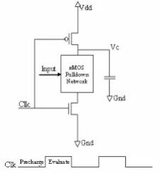
[image:1.595.388.501.475.598.2]The dynamic logic is due to use the capacitive output of the transistor to store a charge and thus remember a logic level for later use [5]. The output decays with time unless it is refreshed periodically since it is stored in a capacitor. Dynamic logic gates also known as clocked logic gates, are used to decrease complexity, increase speed and lower power dissipation. The dynamic design eliminates one of the switch networks from a complementary logic circuit, thus reducing then number of the transistor required to realize a logic function by almost 50%. Figure 1 shows the basic structure of dynamic CMOS logic circuitry.
Figure 1: Basic structure of dynamic CMOS logic circuitry
The operation of a dynamic circuit has two phases: a precharge phase and an evaluate phase depending on the state of the clock signal. When clock Clk = 0, the pMOS transistor in the circuit is turned on and the nMOS transistor is turned off, and the load capacitance is charged to Vdd.
This is called precharge phase. The precharge should be long enough for the load capacitance to completely charge to Vdd. During the precharge phase, the nMOS transistor is
turned off, no conducting path exist between Vdd and
2.1 Conventional CMOS Dynamic Inverter
Conventionally CMOS circuits are pathologically nonadiabatic. Capacitive nodes are rapidly charged and discharged (the energy transfer) through MOS devices (dissipative medium). At times, the full supply potential appears across the channel of the devices and resulting in high device current and energy dissipation.
[image:2.595.106.223.291.388.2] [image:2.595.383.504.406.540.2]A conventional dynamic CMOS inverter is shown in Figure 2. When the clock, Clk is low, the pMOS transistor is on and the output is precharged to logical 1. During the evaluation phase, the clock is high and the output capacitor conditionally discharges if the input to the inverter is logical 1. The charging and discharging are abrupt and hence nonadiabatic in nature. There is also some energy dissipation due to current flowing from supply to ground due to the n-transistor and p-transistors being simultaneously on for a short period of time.
Figure 2: Conventional CMOS dynamic inverter
2.2 Adiabatic Dynamic Logic Inverter
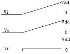
The operation of adiabatic dynamic logic inverter is supplied with clock. The clock or the supply voltage swings are shown in Figure 4. The precharge phase is defined by the clock swing from zero to Vdd when the diode is turned on
and the output voltage Vout follows the clock swing to Vdd -
VD, where the VD is the voltage drop across the diode. In the
evaluate phase, the clock voltage ramps down from Vdd to
zero. In this condition, the diode is reverse bias condition and the output will follow the clock down to zero if Vin is
high. Else, if Vin is low, the output capacitance retains the
charge stored on it [4].
Figure 3: Adiabatic dynamic logic inverter
Figure 4: Associated clock, input, and output waveforms of adiabatic dynamic inverter
2.3 Cascaded Gates
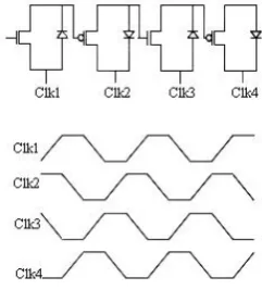
Adiabatic circuit operation requires that only small potential appear across the channel of a device while it is conducting. This must be taken into consideration when interconnecting gates, as it implies that devices should never turn on while there is a nonzero voltage present across the device channel. Between precharge and evaluate, there are only small potential differences present in the ADL inverter circuit: both clock-supply and output nodes are near Vdd. Clock signal must be modified to include a stage of constant voltage of Vdd between the precharge and the evaluate phase so that the input voltage can safely make a transition without making a nonadiabatic transition within the circuit [4]. A constant voltage stage 0V is added between evaluate and precharge to ensure that the output is latched for a finite time and be sampled by the next stage [3]. The clock waveform along with interconnected ADL inverters is shown in Figure 5.
To connect two logic gates, it is necessary to synchronize their respective clock supplies such that when the output of the first stage is latched, the second stage starts evaluating. Another consideration is that when the first stage is evaluating, the second stage should not undergo any nonadiabatic transition [1]. Four clock phases are necessary for cascading such gates because there are four stages in a clock cycle, it is necessary to place four gates in series before the last gate can feed the first one.
Figure 5: Cascaded ADL gates
2.4 Clock Voltage Consideration
A requirement of the particular system of gate interconnection that have been described is that when a gate is in its precharge state, the voltage present at its output must be such that it not turn on the input device of the subsequence gate (VD <Vth). In the case of the precharge
high gate, if the precharge voltage (Vdd−VD) is less than the
turn on point of the subsequence p-type device (VD−Vth), it
will turn on the input p-device of the subsequent gate during prechagre. There are two methods to avoid this problem. The first is to ensure that the forward drop of the diode VD is
less than the threshold voltage Vth of the p-type or n-type
[image:2.595.129.199.574.629.2] [image:2.595.111.215.674.735.2]2.5 Adiabatic Charging
Figure 6: Inverter equivalent when the capacitor C is being charged through the device of on-resistance R
Switching circuits that charge and discharge their load capacitance adiabatically are said to use adiabatic switching [1]. Adiabatic switching can be achieved by ensuring that the potential across the switching devices is kept arbitrarily small which causes a minimal amount of power is consumed as heat [7]. Adiabatic charging may be achieved by charging the capacitor from a time varying source, as shown in Figure 7. This source has an initial value ofVi =0. The ramp increases towards Vdd at a slow rate that ensures
c i
r V V
V = − is kept arbitrarily small. This rate is set by ensuring that the period of the ramp T>>RC.
2 2
2
dd
dd CV
T RC RT T CV RT I
Ediss ⎟
⎠ ⎞ ⎜ ⎝ ⎛ = ⎟ ⎠ ⎞ ⎜ ⎝ ⎛ =
= (1)
A linear increase in T causes a linear decrease in power dissipation. Adiabatic discharge can be arranged in a similar manner with a descending ramp. If T is sufficiently larger than RC, energy dissipation during chargingEdiss→0, and so
the total energy removed from the supply is 2
2 1
dd
CV , the
minimum required to charge the capacitor and hence hold the logic state.
[image:3.595.404.510.137.259.2]This energy may be removed from the capacitor and returned to the power supply adiabatically by ramping Vi back down from Vdd to 0V [2]. As the result, given a suitable supply, it should be possible then to charge a discharge signal node capacitances with only small energy dissipation. This amount of energy is dissipated regardless of the construction of the network and the time taken to complete the charging [8]
Figure 7: Voltage waveform present in the equivalent circuit when charging the capacitor from 0V to Vdd in an adiabatic
manner.
3. Methodology
[image:3.595.335.560.555.678.2]3.1 Truth table
Table 1: Truth table of 1-bit full adder
3.2 Boolean Function
From truth table, the Boolean function for SUM and CARRY can be obtained.
C B A C B A C B A ABC
SUM= + + +
(2)
=C
(
AB+AB) (
+C AB+AB)
=A⊕B⊕C
CARRY=AB+AC+BC
(3)
=AB+C(A+B)
The carry is used to generate the sum output, so the output can be expressed as
SUM=ABC+(A+B+C)CARRY
(4)
=ABC+(A+B+C)(AB+C(A+B))
3.3 Euler Paths
A compact and efficient method to design layouts for complex gates is to place all the transistor gates on one long strip of diffusion. This can be done by using the Euler Paths. An Euler path is a path where all transistors are passed once and only once respective. However, a node can be visited several times.
[image:3.595.106.222.621.710.2]Figure 8(a): Euler path for part 1
Figure 7(b): Euler path for part 2
3.4 Stick Diagrams
A stick diagram is a simplified layout form which does contain the information related to each of the process steps, but does not contain the actual size of the individual features. Instead the features are represented by simple lines hence the name stick diagram. The stick diagram can easily be drawn by hand and is a handy intermediate form between the circuit diagram and the physical layout since it can easily be modified and corrected. It can therefore be used to anticipate and avoid possible problems when laying out the circuit.
clk1 sum 3 clk1 3 clk1 5 4 sum
Carry
1 carry clk 2 1 clk
Sum
carry CLK1
CLK
[image:4.595.353.532.92.222.2]Ab Bb Cb
Figure 9: Stick diagram of Adiabatic Dynamic Full Adder
4. Results
[image:4.595.125.202.93.169.2]4.1 Inverter
Figure 10: Output of Adiabatic Dynamic Inverter
As shown in graph of Figure 10, A representing the input and Vout representing the output of the inverter. The
power dissipated by the adiabatic dynamic inverter is 27
10 08 .
8 x − Watts.
4.2 Nand
Figure 11: Output of Adiabatic Dynamic Nand
Figure 11 shows the output of the Adiabatic Dynamic Nand. The power dissipated by the Adiabatic Dynamic Nand is 26
10 62 .
1 x − Watts.
[image:4.595.359.533.342.460.2]4.2 Nor
Figure 12: Output of Adiabatic Dynamic Nor
Figure 12 shows the schematic and layout of Adiabatic Dynamic Nor. The power dissipated by the Adiabatic Dynamic Nor is approximate to zero.
4.3 1 Bit Full Adder
[image:4.595.91.240.346.471.2] [image:4.595.65.253.554.685.2] [image:4.595.335.551.571.753.2]Figure 13(b): Output of Conventional 1 Bit Full Adder
Figure of 13(a) shows the layout of the conventional 1 Bit Full Adder. The size of the transistor, L/W = 2u/6u for both of the nMOS and pMOS. The output of the adder is shown in the Figure of 13(b), where V (6) represents the output for Carry with the bit 00010111 and V (10) represents the output for the Sum with the bit 01101001. The power dissipated by conventional full adder is 233p Watts.
4.4 Adiabatic Dynamic 1 Bit Full Adder
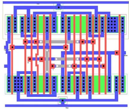
Figure 14(a): Layout of Adiabatic Dynamic 1 Bit Full Adder
Figure 14(b): Output of Adiabatic Dynamic 1 Bit Full Adder
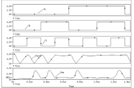
The Figure of 14(a) shows the layout of the Adiabatic Dynamic Full Adder. There are two clocks needed to synchronize the circuit. The clocks are ramp function, different in phase of 90 degrees; 5V and the frequency of 27 MHz. Clocks are denoted as Clk and Clk1. Figure 14(b) shows the results of the Adiabatic Dynamic 1 Bit Full Adder. The output of the Carry is denoted as V (1) with the output bit 00010111 while the output of the Sum is denoted as V (4) with the output bit 01101001. The size of the transistor L/W = 2u/22u for both pMOS and nMOS. The power dissipated by the Adiabatic Dynamic 1 Bit Full Adder is 26
10 23 .
3 x − Watts.
Table 2: Power dissipation comparison of conventional and adiabatic dynamic logics
Power Dissipation
Circuit Conventional (Watts)
Adiabatic Dynamic technique (Watts) Inverter 25.1x10⁻¹² 8.08x10⁻²⁷ NAND 25.1x10⁻¹² 1.62x10⁻²⁶
NOR 50.1x10⁻¹² 0
Full Adder 233x10-12 3.23x10⁻²⁶
5. Conclusion
Based on the outputs of SPICE simulation, it can be concluded that the logics and the circuits which operated in the adiabatic regime, dissipated a very small of power where it could reduce the power dissipation more than 90%. This small dissipation is due to the recycle of charge at the output nodes and also the reduction of number of transistors about 50 percent. The main objective for reducing the power dissipation had been successfully achieved. Unfortunately, there is one critical problem in the adiabatic dynamic technique that is the clock consideration. The circuits will only functioning properly if the appropriate clocks are applied. It also stops working at high-speed systems and only suitable for the applications that requires extremely low energy dissipation. All of the logics and full adder circuit using the adiabatic technique were successfully tested at the frequency of 27 MHz.
REFFERENCES
[1] Dickinson, A.G., Denker, J.S. (May 1994). “Adiabatic Dynamic Logic”, IEEE, 282 – 285.
[2] Dickinson, A.G., Denker, J.S. (March 3, 1995). “Adiabatic Dynamic Logic”, IEEE, 311– 315.
[3] Friedman, V., Liu, S. (Apr 2, 1984). “Dynamic Logic CMOS Circuits”, IEEE, 263 – 266.
[4] Akers, L.A. , Suram, R.( Aug 2002). “Adiabatic Circuits for Low Power Logic”, IEEE, 286 – 289.
[5] Hashizume, M., Sato, M., Yotsuyanagi, H., Tamesada, T.( Jan 2002). “Power Supply Circuit for High Speed Operation of Adiabatic Dynamic CMOS Logic Circuits”, IEEE, 459 – 461.
[image:5.595.317.567.251.339.2] [image:5.595.87.240.350.579.2] [image:5.595.55.276.615.760.2][7] Hee-sup Song , Jin-ku Kang . (Aug 2004). “A CMOS Adiabatic Logic for Low Power Circuit Design”, IEEE, 348 – 351.
[8] Suhwan Kim. , Papaefthymiou, M.C. (Feb 2001). “True single-phase adiabatic circuitry”, IEEE, 52 – 63.
[9] Voss. B., Glesne. M. (Dec 2000). “Adiabatic charging of long interconnects”, IEEE, 835 – 838.
[10] Soudris. D., Pavlidis. V., Thanailakis. A. (Sept. 2001). “Designing low-power energy recovery adders based on pass transistor logic”, IEEE, 777 – 780.
[11] Sung Mo Kang , Lemblebigi.Y. (1999). “CMOS Digital Integrated Circuits”, McGraw-Hill, United State of America.
[12] Neil H.E Weste, Eshraghian. K. (1994). “Principles of CMOS VLSI Design”, Addison - Wesley Publishing Company, United State of America.
[13] Kaushik Roy, Sharat C. P. (2000). “Low Power CMOS VLSI Circuit Design”, John Wiley & Sons, INC, United State of America.