Motorola reserves the right to make changes without further notice to any products herein to improve reliability, function or design. Motorola does not assume any liability arising out of the application or use of any product or circuit described herein; neither does it convey any license under its patent rights nor the rights of others. Motorola products are not designed, intended, or authorized for use as components in systems intended for surgical implant into the body, or other applications intended to support or sustain life, or for any other application in which the failure of the Motorola product could create a situation where personal injury or death may occur. Should Buyer purchase or use Motorola products for any such unintended or unauthorized application, Buyer shall indemnify and hold Motorola and its officers, employees, subsidiaries, affiliates, and distributors harmless against all claims, costs, damages, and expenses, and reasonable attorney fees arising out of, directly or indirectly, any claim of personal injury or death associated with such unintended or unauthorized use, even if such claim alleges that Motorola was negligent regarding the design or manufacture of the part.
1
VREG
Block User Guide
V01.01
Original Release Date: 21 FEB 2001 Revised: 4 MAR 2002
Motorola, Inc
F
re
e
sc
a
le
S
e
m
ic
o
n
d
u
c
to
r,
I
For More Information On This Product, Go to: www.freescale.com
n
c
.
VREG Block User Guide V01.01
2
Revision History
Version Number
Revision Date
Effective
Date Author Description of Changes
0.1 2/21/01 2/21/01 VREG spec moved to SRS2.0 compliant format
1.0 4/05/01 4/05/01 Minor update, spec version number reflects clearcase label V01.00 7/27/01 7/27/01 Document names have been added
Names and Variable definitions have been hidden
V01.01 3/4/02 3/4/02 Changed Document Number
F
re
e
sc
a
le
S
e
m
ic
o
n
d
u
c
to
r,
I
Freescale Semiconductor, Inc.
For More Information On This Product, Go to: www.freescale.com
n
c
.
3
Table of Contents
Section 1 Introduction
1.1 Overview. . . .9
1.2 Features . . . .9
1.3 Modes of Operation . . . .9
1.4 Block Diagram . . . .10
Section 2 Signal Description
2.1 Overview. . . .112.2 Detailed Signal Descriptions. . . .11
2.2.1 VDDA, VSSA . . . .11
2.2.2 VDDR . . . .11
2.2.3 VDD1,[2], VSS1,[2] . . . .11
2.2.4 VDDPLL, VSSPLL . . . .11
2.2.5 VREGEN . . . .12
Section 3 Memory Map and Registers
3.1 Overview. . . .13Section 4 Functional Description
4.1 General. . . .154.1.1 Reference Generation . . . .15
4.1.2 Operational Amplifier . . . .15
4.1.3 Power Output Stage. . . .15
4.1.4 Power On Reset Pulse Generation . . . .15
F
re
e
sc
a
le
S
e
m
ic
o
n
d
u
c
to
r,
I
For More Information On This Product, Go to: www.freescale.com
n
c
.
VREG Block User Guide V01.01
4
F
re
e
sc
a
le
S
e
m
ic
o
n
d
u
c
to
r,
I
Freescale Semiconductor, Inc.
For More Information On This Product, Go to: www.freescale.com
n
c
.
5
List of Figures
Figure 1-1 VREG Block Diagram . . . .10
F
re
e
sc
a
le
S
e
m
ic
o
n
d
u
c
to
r,
I
For More Information On This Product, Go to: www.freescale.com
n
c
.
VREG Block User Guide V01.01
6
F
re
e
sc
a
le
S
e
m
ic
o
n
d
u
c
to
r,
I
Freescale Semiconductor, Inc.
For More Information On This Product, Go to: www.freescale.com
n
c
.
7
List of Tables
Table 2-1 Signal Properties . . . .11
F
re
e
sc
a
le
S
e
m
ic
o
n
d
u
c
to
r,
I
For More Information On This Product, Go to: www.freescale.com
n
c
.
VREG Block User Guide V01.01
8
F
re
e
sc
a
le
S
e
m
ic
o
n
d
u
c
to
r,
I
Freescale Semiconductor, Inc.
For More Information On This Product, Go to: www.freescale.com
n
c
.
9
Section 1 Introduction
1.1 Overview
The VREG block is used to generate the supply voltage (2.5V typ.) of the core logic and memory blocks out of the chip supply voltage (5V typ.).
1.2 Features
The block name includes these distinctive features:
• linear voltage regulator with two independent outputs
• power on reset signal generation
1.3 Modes of Operation
VREG can operate in three different modes
• RUN
In run mode both regulating loops of the voltage regulator are active. This mode is selected whenever the CPU is neither in stop nor in pseudo stop mode and VREGEN is pulled high.
• STANDBY
Standby mode is selected when the CPU is in stop or pseudo stop mode and VREGEN is pulled high. In standby mode the gates of the power transistors are directly connected to the reference voltage. In this case the voltage regulator acts as a voltage clamp. While in standby mode, the effective inner resistance of the regulator is increased, the quiescent current consumption of the regulator itself is heavily decreased.
• SHUTDOWN
Shutdown mode is only available, when the device is equipped with a VREGEN bit. Shutdown mode is selected by tieing VREGEN to ground. In this case, the core logic must be supplied from external by applying 2.5V(+/-10%) on VDD and VDDPLL. The power on reset pulse generation circuit is not affected by selecting shutdown mode.
F
re
e
sc
a
le
S
e
m
ic
o
n
d
u
c
to
r,
I
For More Information On This Product, Go to: www.freescale.com
n
c
.
VREG Block User Guide V01.01
10
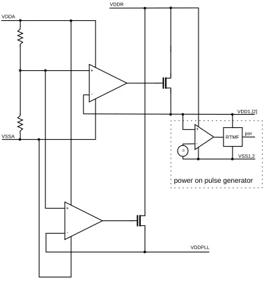
[image:10.612.122.501.192.602.2]1.4 Block Diagram
Figure 1-1 is a block diagram of the VREG.
Figure 1-1 VREG Block Diagram
+
-+
-VDD1,[2]
VSS1,2
VDDPLL VDDA
VSSA
VDDR
=
RTMF por +
-power on pulse generator
F
re
e
sc
a
le
S
e
m
ic
o
n
d
u
c
to
r,
I
Freescale Semiconductor, Inc.
For More Information On This Product, Go to: www.freescale.com
n
c
.
11
Section 2 Signal Description
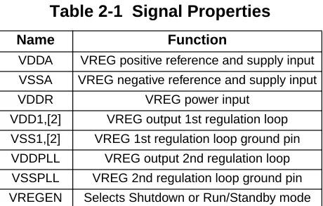
[image:11.612.192.422.157.304.2]2.1 Overview
Table 2-1 lists all pins associated with the VREG block.
2.2 Detailed Signal Descriptions
2.2.1 VDDA, VSSA
VREG uses the VDDA/VSSA supply pin pair to supply the voltage regulator and to derive the reference
voltage. The reference voltage VREG is regulating to is (VDDA - VSSA)/2.
2.2.2 VDDR
VDDR is the power input to the voltage regulator. The output current of the two regulating loops is drawn out of this pin.
2.2.3 VDD1,[2], VSS1,[2]
VDD1, VSS1 and optional VDD2, VSS2 are the core logic supply pins. VDD1 and VDD2 are connected internally by metal as well as VSS1 and VSS2. Each power supply pin pair must be externally decoupled with a ceramic capacitor (100nF .. 220nF, X7R ceramic). VDD1,[2] is connected to the output of the first regulating loop of the voltage regulator.
2.2.4 VDDPLL, VSSPLL
VDDPLL and VSSPLL are the oscillator and pll supply pins. This supply pin pair must be externally decoupled with a ceramic capacitor (100nF .. 220nF, X7R ceramic). VDDPLL is connected to the output of the second regulating loop of the voltage regulator.
Table 2-1 Signal Properties
Name Function
VDDA VREG positive reference and supply input VSSA VREG negative reference and supply input
VDDR VREG power input
VDD1,[2] VREG output 1st regulation loop VSS1,[2] VREG 1st regulation loop ground pin VDDPLL VREG output 2nd regulation loop VSSPLL VREG 2nd regulation loop ground pin VREGEN Selects Shutdown or Run/Standby mode
F
re
e
sc
a
le
S
e
m
ic
o
n
d
u
c
to
r,
I
For More Information On This Product, Go to: www.freescale.com
n
c
.
VREG Block User Guide V01.01
12
2.2.5 VREGEN
This optional pin is used to disable the voltage regulator if the core logic as well as the oscillators are supplied from external.
F
re
e
sc
a
le
S
e
m
ic
o
n
d
u
c
to
r,
I
Freescale Semiconductor, Inc.
For More Information On This Product, Go to: www.freescale.com
n
c
.
13
Section 3 Memory Map and Registers
3.1 Overview
The VREG block has no CPU accessible registers.
F
re
e
sc
a
le
S
e
m
ic
o
n
d
u
c
to
r,
I
For More Information On This Product, Go to: www.freescale.com
n
c
.
VREG Block User Guide V01.01
14
F
re
e
sc
a
le
S
e
m
ic
o
n
d
u
c
to
r,
I
Freescale Semiconductor, Inc.
For More Information On This Product, Go to: www.freescale.com
n
c
.
15
Section 4 Functional Description
4.1 General
The VREG block consists of a reference voltage generator, two operational amplifiers, two nmos power output stages and a power on reset pulse generation circuit.
4.1.1 Reference Generation
The reference generation is comprised of a resistor reference ladder between VDDA and VSSA. The
output voltage of the reference ladder (VDDA- VSSA)/2 is fed into both operational amplifiers as regulation
reference.
4.1.2 Operational Amplifier
The operational amplifier compare the reference voltage ((VDDA- VSSA)/2) with the actual output voltage
(vdd or vddpll) to generate the gate voltage of the power output transistors.
In standby mode, the operational amplifiers are disabled and the gates of the power transistors are connected directly to the reference voltage in order to decrease the quiescent current.
4.1.3 Power Output Stage
Each power output stage consists of an nmos power transistor with its drain on VDDR and its source on VDD or VDDPLL.
4.1.4 Power On Reset Pulse Generation
A comparator monitors the actual value of VDD. If VDD is below VPOR, the power on reset signal is
asserted forcing the CPU in the power on reset state.
F
re
e
sc
a
le
S
e
m
ic
o
n
d
u
c
to
r,
I
For More Information On This Product, Go to: www.freescale.com
n
c
.
VREG Block User Guide V01.01
16
F
re
e
sc
a
le
S
e
m
ic
o
n
d
u
c
to
r,
I
Freescale Semiconductor, Inc.
For More Information On This Product, Go to: www.freescale.com
n
c
.
17
User Guide End Sheet
F
re
e
sc
a
le
S
e
m
ic
o
n
d
u
c
to
r,
I
For More Information On This Product, Go to: www.freescale.com
n
c
.
VREG Block User Guide V01.01
18
FINAL PAGE OF
18
PAGES
F
re
e
sc
a
le
S
e
m
ic
o
n
d
u
c
to
r,
I
Freescale Semiconductor, Inc.
For More Information On This Product, Go to: www.freescale.com
n
c
.