Microstructural Characteristics of InGaZnO Thin Film
Using an Electrical Current Method
Yen-Ting Chen
1, Fei-Yi Hung
1,+, Shoou-Jinn Chang
2, Truan-Sheng Lui
1and Li-Hui Chen
11Department of Materials Science and Engineering, Institute of Nanotechnology and Microsystems Engineering,
Center for Micro/Nano Science and Technology, National Cheng Kung University, Tainan 701, Taiwan, R. O. China
2Institute of Microelectronics & Department of Electrical Engineering, National Cheng Kung University,
Tainan 701, Taiwan, R. O. China
This research studied the microstructural characteristics and electronic properties of IGZO1114films (atomic ratio In : Ga : Zn : O= 1 : 1 : 1 : 4) with different annealing conditions. The solid-state electrical current method was used in the IGZO/Infilms (In layer was a channel) and the interface effect on the electrical current mechanism was discussed. The experimental results show the effect of the annealing temperature was larger than that of the deposition oxygenflow rate for thefilm resistances. IGZOfilm which was annealed at 575 K was able to stabilize the composition of the matrix. The electrical current experiment at room temperature confirmed that the diffusion of the IGZO/Infilm occurred through an electric current induced crystallization (EIC). The In layer not only assisted the recrystallization behavior of the IGZOfilm, but also improved the electrical resistance. [doi:10.2320/matertrans.M2011312]
(Received October 7, 2011; Accepted January 6, 2012; Published March 25, 2012)
Keywords: InGaZnO, crystallization, electric current induced crystallization (EIC), electrical resistance
1. Introduction
InGaZnO (IGZO) is one of the most attention-getting oxide semiconductor materials, and it is also an excellent amorphous oxide semiconductor (AOS).13) It has higher electron motility (more than 10 cm2V¹1s¹1) in the deposited conditions at room temperature and has applications for low-temperature devices.3,4)The IGZO system has been reported constantly, and most of the reports have focused on the relationship between the atomic ratio and device character-istics.25) Furthermore, many papers have discussed the annealing effects of IGZO thin films, but the depositing oxygenflow conditions affecting thefilm matrix have still not been examined.6) Notably, these papers reported that the chemical composition of the IGZO films is not stable, and there are still reliability problems in the interface zone of devices.7)
Both the composition and annealing temperature of IGZO thinfilms affect thefilm resistance and interface problems,57) so stable IGZO thin film characteristics were obtained by using the co-sputtering system to deposit thin films and the samples were annealed with different depositing oxygenflow rates.8,9) In fact, most single thin film systems have better electrical properties after an annealing treatment at 675 875 K for 12 h. For a double layer structure, high temper-ature annealing always decreases the reliability in the interface zone due to interface diffusion.7,9,10) Electrical current testing is a low temperature process carried out in atmosphere.11)Its mechanism is an electrical current induced crystallization (EIC)12,13)that has been largely ignored in the optoelectronic thin films until now. So, the present study performed electrical current experiments on In thin film to discuss the electrical current crystallization characteristics of the IGZO/In structure at low temperature (During electrical current testing, the surface temperature of thefilm was raised by joule heat and was<455 K).
Based on the above, this study used IGZO111416)(atom ratio of In : Ga : Zn : O=1 : 1 : 1 : 4) thin films to inves-tigate the effects of both the annealing temperature and depositing oxygen flow rate. Then we analyzed the crystallization characteristics of the IGZOfilms and interface diffusion effects by an electrical current testing with IGZO/In thinfilms. For actual applications, the interface of Au/IGZO in the Au/IGZO/In structure was also observed. The results not only provide reference for recent TFT devices, but also clarify the interface atomic behavior and the electrical current induced crystallization (EIC) mechanism.
2. Experimental Procedure
2.1 Structural analysis of InGaZnO4film
InGaZnO4 (atom ratio In : Ga : Zn : O=1 : 1 : 1 : 4) thin films were deposited on the glass substrates using a co-sputter (ULVAC, Model ACS-4000-C3). The sputtering power was 100 W and the depositing operating pressure was 2 Pa. For the sputter depositing duration, we maintained the Ar gas flow rate at 20 sccm and controlled the O2 gas
flow rate for 0, 0.1, 2 and 5 sccm individually. In addition, some samples were annealed in a vacuum at 475, 525 and 575 K for 1 h respectively. The resistance of the films was measured using Hall effect measurement before and after annealing.11)
According to the data of electric resistance, three samples A, B and C (A sample: O2 flow rate is 0 sccm; annealing temperature is 575 K, B sample: O2 flow rate is 5 sccm; without annealing, C sample: O2flow rate 5 sccm; annealing temperature is 575 K) were subjected to X-ray and electron spectroscopy for chemical analysis (ESCA) to analyze the phase composition and the depth composition of the IGZO thin films. The Cu-K¡ standard (=1.5403 nm) was used, the scanning angle was varied from 20 to 90° and the scanning velocity was 2°·min¹1. In addition, Raman spec-troscopy of sample A was carried out with laser wavelength 523 nm and scanning range 300 to 700 cm¹1.
2.2 Electric current test of InGaZnO/In structure
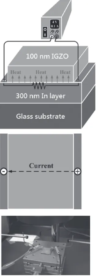
The thickness of the Indium (In) conductive layer was about 300 nm on the glass substrates by sputtering. The sputtering parameters of the Infilm were 80 W for sputtering power, depositing Ar flow rate for 20 sccm and operating pressure for 2 Pa. Then InGaZnO4 film was deposited about 100 nm on the In conductive layer and finally fabricated an InGaZnO4/In/Glass thin film [The structure is shown in Fig. 1(a)].
The IGZO4sputtering parameters were 100 W for sputter-ing power, depositsputter-ing O2/Ar flow rate for 0/20 sccm and operating pressure for 2 Pa. Next, an electrical current test with a probe electrify meter [Fig. 1(b), the In film is an electric layer] was performed, and the voltage and current were within 2.0 V and 0.32 A in atmosphere (breakdown voltage of the In film was 2.8 V). Finally, the electrical resistivity of thefilms before and after electrical current test was measured using the Hall effect measurement at room
temperature with indium ohmic contacts. Also, the diffusion behavior at the interface zones was examined using electron spectroscopy for chemical analysis (ESCA). For the Au/ IGZO/In structure, the thickness of the Au film was about 50 nm and the interface mechanisms of Au/IGZO were examined using high-resolution transmission electron mi-croscopy (FE-TEM) and energy-dispersive X-rays (EDX).
3. Result and Discussion
3.1 Microstructural characteristics of InGaZnO4films Figure 2 shows the electric resistance of the InGaZnO4
films at the different temperatures of vacuum annealing and the deposited oxygenflow rate. The electric resistance of the
film increases with increasing oxygenflow rate, but decreases as the annealing temperature rises. Also, the influence of the oxygen flow rate becomes smaller when the annealing temperature is higher. Both the annealing temperature and oxygen flow rate can control the electric resistance of the IGZO films effectively. Furthermore, the influence of annealing temperature is larger than the oxygen flow rate for the electric resistance of thefilm. For actual applications, the annealing temperatures are raised as far as possible (<625 K) to increase reliability and workability. So, it is not objective to declare that the electric resistance of the IGZO
films was greatly affected by the depositing oxygen flow rate.9,10) In fact, raising the annealing temperature not only improves the crystallization of thefilm but induces lowerfilm electric resistance. Nevertheless, the TFT glass substrates will become softer and the interfaces of device undergo server diffusion when the annealing temperature is higher than 575 K. For this reason, the IGZO films possess much applicability at 575 K vacuum annealing.
Figure 3 is the XRD pattern of the IGZO1114 films at several different conditions. It shows both the sputtering oxygen flow rate and the 575 K vacuum annealing can change the crystallization of the IGZO films. The crystal phase InGaO3(ZnO)x of low angle of the un-annealed film was found to be at 33°. After annealing, the matrix underwent a phase transform and induced the peak to shift from 33 to 24°. Therefore the two crystal phases caused the difference in Fig. 1 Schematic illustration of electric current experiment for IGZO/In
structure.
102
103
104
105
100W O2 flow rate
0 sccm 0.1 sccm 2.0 sccm 5.0 sccm
Resistance,
R
/
Ω
Annealing Temperature, AT / K
475 525 575
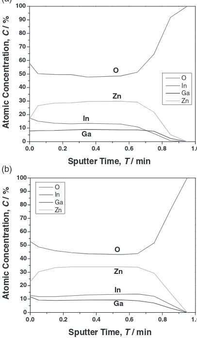
[image:2.595.91.251.74.523.2] [image:2.595.322.534.74.241.2]the electric resistance of the film, and the crystal phase (IGZO4) of 24° was able to decrease the electric resistance of the film.14) After annealing, the matrix of IGZO was still partially amorphous and the XRD peak observed around 2ª=24° was broader. In fact, some InGaZnO and In2O3 crystallized phases had exited.1517) Because both the depositing oxygenflow rate and crystallization can influence the oxygen vacancy defects and thus change the electric resistance of IGZO1114films, the oxygen atom concentration and the atomic composition of depth in the matrix were detected using ESCA to estimate the effect of atomic ratios. Figure 4 is ESCA analysis of the IGZO1114 film after annealing. The concentration of oxygen atoms was larger than the others. In addition, zinc had low adhesion on the deposited film and the concentration was lower. The concentration of the others (In; Ga) was similar.17,18) The annealing without oxygen made the oxygen concentration lower in the matrix [Fig. 4(a)]. Notably, the In atom concentration increased when the film was deposited with oxygen and vacuum annealing was performed [Fig. 4(b)]. This explains why oxygen and the post annealing stabilized the composition of the matrix. This had a positive con-tribution on the optical characteristics of the IGZO1114film. Annealing conditions greatly influenced the properties of the IGZO1114 thin film. The relationship between the crystallization and the atom compositions was investigated by Raman spectroscopy.17,18) The IGZO thin films were produced by the same process (deposited without oxygen) before and after 575 K vacuum annealing to perform Raman spectrum analysis. The results show that no Raman shift peak was found for the un-annealed IGZO thinfilm. On the other hand, a Raman spectrum of the annealed IGZO thinfilm was found and is shown in Fig. 5. Because there is no data about the IGZO Raman shift peak, the peak at Raman shift 466 cm¹1is defined as“CH peak”. The values of the IGO and ZnO Raman shift peaks are also shown in Fig. 5 to compare with the data of the IGZO films.19,20) So the CH peak is confirmed as not belonging to the IGO or ZnO systems. Compared to Figs. 2 and 3, low angle crystal phase (24°: IGZO4) contributed to CH peak of Raman spectrum and affected the electric resistance of thefilm.
3.2 Electrical current induced crystallization of InGaZnO4/Indium structure
After annealing, the IGZO1114 thin films can obtain a stable phase structure, but the high temperature annealing process can easily induce interface diffusion (interface pollution) in devices and severely affect the workability. Electrical current induced crystallization (EIC) is a low
10 20 30 40 50 60 70 80 90 100
(a)
(b) (c)
Intensity
Degree (2θ)
InGaO3(ZnO)X
(220)
InGaZnO (222)
In2O3 (222)
Fig. 3 XRD of IGZO1114 thinfilm: (a) O2/575 K, (b) vacuum/575 K and
(c) O2/un-annealed.
0.0 0.2 0.4 0.6 0.8 1.0
0 10 20 30 40 50 60 70 80 90 100
In
Ga Zn
O In Ga Zn O
(a)
0.0 0.2 0.4 0.6 0.8 1.0
0 10 20 30 40 50 60 70 80 90 100
Ga In Zn O
In Ga Zn
O
(b)
Atomic Concentration,
C
/ %
Atomic Concentration,
C
/ %
Sputter Time, T / min
Sputter Time, T / min
Fig. 4 ESCA profiles of IGZO1114 matrix after vacuum annealig at 575 K: (a)film deposited without oxygen and (b)film deposited with oxygen.
300 400 500 600 700
0 50 100 150 200 250 300 350
IG3(428)
IG2(377)
Intensity
CH(466) IG1(328) E2(435)
Raman Shift, RS / cm-1
Fig. 5 Raman spectroscopy of IGZO4 after vacuum annealing at 575 K.
[image:3.595.323.526.77.425.2] [image:3.595.311.540.478.648.2]temperature process that can not only control the electric resistance of the films, but also avoids the problems of interface pollution can and even improve the crystallization efficiency in a short electrical current duration.11,21)
The present study chose Indium (In) material to be the conductive layer, and then deposited a IGZO1114 thin film to form an InGaZnO(100 nm)/In(300 nm)/glass structure. A loading limit between the voltage and the current for EIC testing was measured.1113,21)We controlled the conditions of EIC testing to obtain crystallization and diffusion doping by electron-migration and the joule heat, and then affected the electric resistance and the interface characteristics of the IGZO1114 thin films.
The EIC films will break if the input voltage or power is too large. So a power loading test of the un-annealed IGZO/ In thinfilm was performed. The voltage (V)current (I) curve is shown in Fig. 6. It can be seen that the breakdown voltage of the Infilm is 2.8 V, and the voltage of 2.0 V and the current of 0.32 A was selected for the EIC test. During 30 min of EIC testing (the EIC films were not damage), the surface temperature of the IGZO/In thin film was about 425 K by joule heat. Figure 7 shows that the EIC method decreased the electric resistance of thefilm at lower temperatures.9,10)The joule heat offilm was induced by EIC testing and raised the temperature. The heat source was in the In conductive layer, and the heat transfer direction was toward the upper IGZO
film. Due to the interlayer (In film) being 300 nm thick, the induced joule heat (³425 K) was insufficient to crystallize the as-deposited IGZOfilm. After EIC testing, the degree of crystallization had not only been raised but In had diffused into the as-deposited IGZO film to enhance the electrical properties. Meanwhile, electron-migration occurred in the In interlayer and the diffusion direction of the In ions was both parallel and perpendicular to the electron flow. This is why the IGZO matrix was saturated and higher doping concen-trations were able to decrease the resistivity. Clearly, the In atoms provide a great contribution to diffusion doping under the EIC mechanism.11,21)
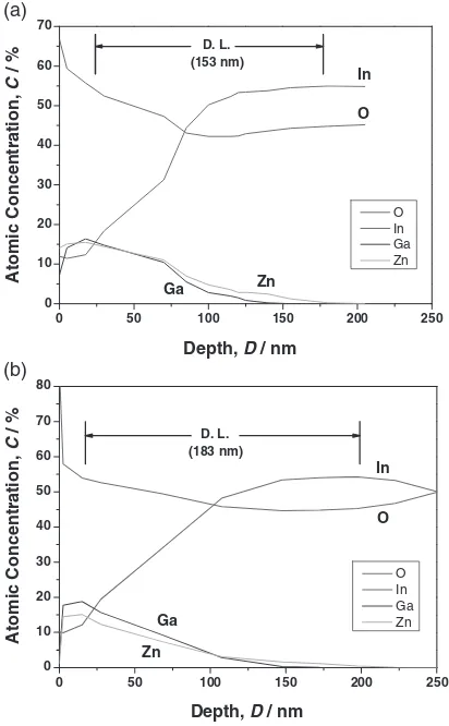
XPS depth profiles of thefilms before and after EIC test are shown in Fig. 8. Notably, the interface diffusion within the IGZO/In structure was confirmed. The border-top of this diffusion layer is where the In atom concentration curve
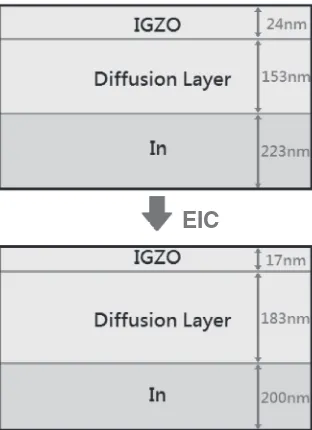
begins rising and the border-bottom is where the Zn atom concentration was zero. After comparison, In atoms diffused into the IGZO matrix and Zn, and Ga atoms diffused into the In layer occurring at the same duration. The thickness of the diffusion layer increased from 153 to 183 nm after EIC testing. In fact, there was an original diffusion layer before the EIC test (sputtering effect). This diffusion layer had grown top-ward and bottom-ward during EIC. Figure 9 shows the thickness profile of each layer for the EIC structure, and it also illustrates the interface effect (the IGZO 0.0 0.4 0.8 1.2 1.6 2.0 2.4 2.8 3.2 3.6
0.00 0.05 0.10 0.15 0.20 0.25 0.30 0.35 0.40
Saturated current
Saturated voltage
Current,
I
/A
Voltage, V / V
Fig. 6 The voltage (V)current (I) curve of IGZO/In structures.
IGZO/In EIC-IGZO/In
0.8 1.0 1.2 1.4 1.6 1.8
Resistance,
R
/
Ω
Fig. 7 Electric resistance of IGZO/In structures before and after EIC testing. The surface temperature of IGZOfilm was about 425 K by joule heat and electrical current time was 30 min.
0 50 100 150 200 250
0 10 20 30 40 50 60 70
Zn Ga
In
O In Ga Zn
D. L. (153 nm)
O
(a)
0 50 100 150 200 250
0 10 20 30 40 50 60 70 80
Zn Ga
In
O In Ga Zn
D. L. (183 nm)
O
(b)
Atomic Concentration,
C
/ %
Atomic Concentration,
C
/ %
Depth, D / nm
Depth, D / nm
[image:4.595.54.282.69.241.2] [image:4.595.331.520.71.217.2] [image:4.595.323.529.288.621.2]layer diminished when the diffusion layer grew) related to the electric resistance of the IGZO/In thin film after EIC testing. That is why the electric resistances of this IGZO/ In structure in Fig. 7 were lower than that of the un-EIC
films.
According to the reference9,10) and the above-mentioned results, the EIC mechanism is illustrated in Fig. 10. The electrical current induced diffusion in the interface between the In conductive layer and the IGZO film. When the diffusion layer grew, it not only improved the electric characteristics around the interface area, but also caused the partial crystallization in the IGZOfilm matrix. (When the In atomic concentration increased in the matrix, the rich In2O3 phase would increase.)
When the EIC testing time increased, the diffusion of the joule effect caused the diffusion layer to grow and also enhanced the doping effect in the IGZO film. Thus the
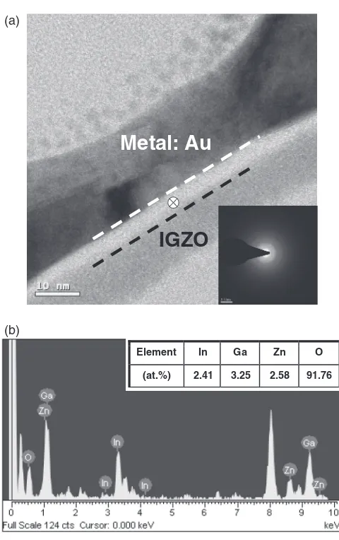
electric characteristics of the IGZO/In structure have an improvement obviously due to the contribution from EIC induced In doping and crystallization in the IGZO matrix. For actual applications, the metal layer and IGZO matrix had interface diffusion after high temperature annealing. Accord-ing to EDX results (Fig. 11), Au atoms were detected in the interface zone (Au/IGZO) and Au atoms diffused into the IGZO matrix. Due to the partial crystallization, low Au atoms could not affect the lattice of the matrix significantly. Notably, the Au/IGZO/In structure was fabricated for EIC testing and the Indium (In) was the conductive layer. After EIC testing, the interface between the Au film and IGZO
[image:5.595.91.247.69.284.2] [image:5.595.308.546.69.310.2] [image:5.595.60.278.340.531.2]film was also observed [Fig. 12(a)] and EDX was found [Fig. 12(b)] that Au atoms did not diffuse into the IGZO matrix (no interface pollution).15,22)In other words, the EIC process caused the IGZO thin films to have the crystal conditions similar to the traditional annealing process, and moreover the structure had a heat diffusion and doping effect. This may provide a reference for the design of device structures.
4. Conclusions
The electric resistance of InGaZnO4 thin film increased with increasing the deposited oxygen flow rate, but raising the vacuum temperature reduced the electric resistance. After 575 K vacuum annealing, a thin film appeared the phase transform. Furthermore, the atomic concentration in the thin
film matrix became stable and a CH peak of Raman shift 466 cm¹1was found after annealing.
EIC testing induced an interface effect of the IGZO/In thin
film and made the diffusion layer grow. This not only improved the electric characteristics around the interface area, but also caused partial crystallization and heat diffusion doping in the IGZO films.
EIC
Fig. 9 Thickness profiles of each layer of EIC structure. The IGZO layer diminished when the diffusion layer grew.
Fig. 10 The schematic illustration of electric current induced doping and recrystallization in IGZO/In structure.
IGZO
Au
IGZO
Au In Ga Zn O
at.% 0.31 2.24 3.64 2.69 91.12
Acknowledgements
The authors are grateful to The Instrument Center of National Cheng Kung University, the Center for Micro/Nano
Science and Technology (D100-2700) and NSC 100-2221-E-006-094; NSC100-2221-E-006-092 for thefinancial support.
REFERENCES
1) Y. K. Moon, S. Lee, D. H. Kim, D. H. Lee, C. O. Jeong and J. W. Park:
JPN J. Appl. Phys.48(2009) 031301-1.
2) G. H. Kim, B. D. Ahn, H. S. Shin, W. H. Jeong, H. J. Kim and H. J. Kim:Appl. Phys. Lett.94(2009) 233501.
3) Y. Kikuchi, K. Nomura, H. Yanagi, T. Kamiya, M. Hirano and H. Hosono:Thin Solid Films518(2010) 3017.
4) M. Nakata, K. Takechi, T. Eguchi, E. Tokumitsu, H. Yamaguchi and S. Kaneko:JPN J. Appl. Phys.48(2009) 081607.
5) D. P. Gosain and T. Tanaka:JPN J. Appl. Phys.48(2009) 03B018.
6) H. Godo, D. Kawae, S. Yoshitomi, T. Sasaki, S. Ito, H. Ohara, H. Kishida, M. Takahashi, A. Miyanaga and S. Yamazaki:JPN J. Appl. Phys.49(2010) 03CB04.
7) K. Takechi, M. Nakata, T. Eguchi, H. Yamaguchi and S. Kaneko:JPN J. Appl. Phys.48(2009) 011301.
8) J. Lee, J. S. Park, Y. S. Pyo, D. B. Lee, E. H. Kim, D. Stryakhilev, T. W. Kim, D. U. Jin and Y. G. Mo:Appl. Phys. Lett.95(2009) 123502.
9) S. Y. Lee, S. Chang and J. S. Lee:Thin Solid Films518(2010) 3030.
10) A. Sato, M. Shimada, K. Abe, R. Hayashi, H. Kumomi, K. Nomura, T. Kamiya, M. Hirano and H. Hosono:Thin Solid Films518(2009) 1309.
11) F. Y. Hung:Mater. Trans.52(2011) 11381141.
12) H. C. Chuang, F. Y. Hung, T. S. Lui and L. H. Chen:Mater. Trans.52
(2011) 2530.
13) F. Y. Hung, Z. R. Wang, T. S. Lui and L. H. Chen:Mater. Trans.46
(2005) 18201824.
14) B. D. Ahn, H. S. Shin, G. H. Kim, J. S. Park and H. J. Kim:JPN J. Appl. Phys.48(2009) 03B019.
15) I. K. Jeong, H. L. Park and S. I. Mho:Solid State Commun.108(1998) 823826.
16) Y. Sun and J. A. Rogers:Adv. Mater.19(2007) 18971916.
17) K. Inoue, K. Tominaga, T. Tsuduki, M. Mikawa and T. Moriga:
Vacuum83(2009) 552556.
18) J. A. Jeong and H. K. Kim:Thin Solid Films519(2011) 32763282.
19) J. H. Zheng, Q. Jiang and J. S. Lian:Appl. Surf. Sci.257(2011) 5083 5087.
20) N. Tripathi, K. Vijayarangamuthu and S. Rath:Mater. Chem. Phys.126
(2011) 568572.
21) K. J. Chen, F. Y. Hung, T. S. Lui, S. J. Chang and Z. S. Hu:Mater. Trans.52(2011) 15601564.
22) S. Hwang, J. H. Lee, C. H. Woo, J. Y. Lee and H. K. Cho:Thin Solid Films519(2011) 51465149.
(a)
(b)
Element In Ga Zn O
(at.%) 2.41 3.25 2.58 91.76