Computer Simulation of Precipitation Process in Si
/
Ge Amorphous
Multi-Layer Films: Effects of Cu Addition
Yasushi Sasajima
1,2,+, Junya Murakami
3and Ahmad Ehsan Bin Mohd Tamidi
31Department of Materials Science and Engineering, Faculty of Engineering, Ibaraki University, Hitachi 316-8511, Japan 2Frontier Research Center for Applied Atomic Sciences, Ibaraki University, Naka-gun, Ibaraki 319-1106, Japan
3Graduate School of Science and Engineering, Ibaraki University, Hitachi 316-8511, Japan
We have simulated the precipitation process in an amorphous Si/Ge multi-layerfilm, with and without Cu addition, by a molecular dynamics method. Four specimens were prepared for this study: Si/Ge layers, Si/(Ge+Cu) layers, (Si+Cu)/(Ge+Cu) layers and Si/Cu/Ge/ Cu layers. After the multi-layeredfilms became amorphous, we tracked the movement of individual atoms at 1000 K, the annealing temperature. When Cu was present in the Ge layer or both the Si and Ge layers, the precipitation of nano-clusters was less than that in Cu-free Si/Ge layers. We think that the Cu atoms block the precipitation and make the Si and Ge become more stable in the amorphous state. If Cu atoms are note present in a layer, however, like the Si layer in Si/(Ge+Cu) and Si/Cu/Ge/Cu specimens, the precipitation of nano-clusters in the Cu-free layer is enhanced. Therefore we conclude that precipitation of nano-clusters in Si/Ge layers can be controlled by how Cu atoms are added to the amorphous Si/Ge system, and that this will improve the thermoelectric performance. [doi:10.2320/matertrans.M2013191]
(Received May 24, 2013; Accepted July 22, 2013; Published September 6, 2013)
Keywords: precipitation process, computer simulation, amorphous silicon/germanium multi-layerfilm, copper addition
1. Introduction
People in Japan have become even more interested in renewable and conservation energy techniques after their experiences in the summer months following the massive earthquake and tsunami that struck northeastern Japan in March 2011 and led to the Fukushima nuclear accident, when the government implemented various energy saving measures to compensate for the loss of nuclear power-generated electricity. These techniques should be environmentally conscious. Using thermoelectric materials is one energy
conservation technique. Approximately 90% of the world’s
electricity is generated by heat energy, typically operating at
3040%efficiency, thus losing massive amounts of power in
the form of heat released to the environment.1) Therefore,
extracting energy from waste heat by using thermoelectric materials is a promising approach.
Thermoelectric materials are materials that can transfer
heat into energy. Efficiency of these materials depends on the
figure of merit, ZT,
ZT ¼¡µ¬2T; ð1Þ
where T, ¡, µand ¬ are the absolute temperature, Seebeck
coefficient, electrical resistivity and thermal conductivity,
respectively. Silicongermanium alloys are currently the best
thermoelectric materials around 1000 K. Usability of SiGe
alloys is, however, limited by their high price and theirZTis
also only in the mid-range.
It has been reported that high thermoelectric power
(Seebeck coefficient) is present only when recrystallization
of nanocrystals occurs in the thinfilm. These nanocrystals are
formed by the metal-induced crystallization (MIC) effect of the dopant metals. MIC is a phenomenon where dopant metal atoms lower the recrystallization temperature of an
amor-phous semiconductor.2) This suggests that superior
thermo-electric properties will arise from the nanocrystals in the
amorphous matrix.3,4) If this consideration is correct,
nano-crystals should be generated in the Si/Ge system to achieve
superior thermoelectric properties.
Unfortunately, in the experiment conducted by Takiguchi
et al.3) when they attempted to make a Si/(Ge+B)
superlattice thin film, there was no sign of the MIC effect.
In fact, high thermoelectric power (>1 mV K¹1) was
observed in the superlattice thinfilm only when nanocrystals
(¯10 nm) were present; however, limitations of the specimen
preparation system and the use of B as the dopant made
it difficult to prepare specimens with a precisely controlled
nanostructure.
In this paper, we report our research using computer
simulation on the effect of Cu dopant in Si/Ge amorphous
multi-layerfilms. We used a molecular dynamics calculation
method to obtain a meta-stable structure of the specimen. We
used Cu-free and Cu-added multi-layer films of Si and Ge
with an amorphous structure, and then we annealed thefilms
to generate nano-clusters. We analyzed the behavior of the precipitation of nano-clusters by extracting the atoms with the same coordination number as the bulk in the obtained structure.
2. Simulation Method
In this study, we prepared four types of specimens:
multi-layers of Si/Ge, Si/(Ge+Cu), (Si+Cu)/(Ge+Cu) and
Si/Cu/Ge/Cu, where “+Cu” means that Cu atoms were
added into Si and Ge layers as substitutional atoms and “/”
indicates layers. The first, second and third multi-layer
films contained the same numbers of unit cell, ten in the
h100i and h010i directions and six in the h001i direction,
where the lattice constant of the unit cell was set to be the average of the lattice constants of Si and Ge. The dimensions
of the unit cell were 5.54 nm in the h100i and h010i
directions and 3.33 nm in the h001i stacking direction of the multi-layers. On the other hand, the fourth specimen had
ten unit cells in the h100i and h010i directions and eight
unit cells in theh001idirection. Due to the different number
of unit cells in the h001i direction, this specimen was
4.43 nm long in the stacking direction of the multi-layers.
The first specimen contained only Si and Ge, described as
Si/Ge. In the second specimen, we added Cu to only the
Ge layer at the ratio of Ge : Cu=6 : 4, described as Si/
(Ge+Cu). In the third specimen, we add 20 at% of Cu
to both the Si and Ge layers, described as (Si+Cu)/
(Ge+Cu). The fourth specimen, we formed a thin Cu layer
at each Si and Ge interface, described as Si/Cu/Ge/Cu.
Side views of the four types of specimens from the [010] direction are shown in Fig. 1.
To calculate the interaction between these atoms, we used
the extended Tersoff potential.5)This is one of the families of
potentials developed by Tersoff,6,7) and it is based on the
concept of bond order: the strength of a bond between two atoms is not constant, but depends on the local environment. Moreover, this potential has been proven to be reliable, and it is widely used recently. The periodic boundary conditions
were imposed in all the directions, h100i,h010i and h001i.
The Verlet algorithm was used for the calculation of atomic
movement,8)while the discrete time¦t was set as 0.3 fs. The
book-keeping and cell-index methods were used to reduce
computing time.9) First, all four specimens were melted at
a temperature 5000 K and quenched at 4.2 K. The time durations of them were both 9 fs. After the multi-layered
films became amorphous, we tracked the movement of
individual atoms at 1000 K, the annealing temperature, for 7200 fs. For the atomic structures before and after the annealing process, the distributions of the four-coordination atoms were calculated.
3. Results and Discussion
In this study, we used Si/Ge as the reference system.
We compared the four specimens to each other to determine
how Cu affects the precipitation of nano-clusters in Si/Ge
amorphous multi-layer films. After that, we counted the
numbers of four-coordination atoms in every 0.2 nm interval
of the layers from bottom to top along the h001i direction.
Then, by checking which layer had more four-coordination atoms, we could identify which parts of the system had more nano-cluster precipitates. Takiguchi’s previous experimental
results10) showed that the size of the precipitated
nano-clusters in the Si/Ge amorphous multi-layered films would
be around 6 nm in diameter. This size is too large compared to the present calculation. However, it is possible to deduce important information about the precipitation process in the
multi-layer films.
The results were visualized to observe the precipitation of nano-clusters. Figure 2 shows the images of all atoms (left) and the four-coordination atoms (right), in amorphous state,
for the specimens of (a) Si/Ge, (b) Si/(Ge+Cu) with
Ge : Cu=6 : 4, (c) (Si+Cu)/(Ge+Cu) with 20 at% Cu
concentration in both the layers and (d) Si/Cu/Ge/Cu.
In contrast, Fig. 3 shows all atoms (left) and the four-coordination atoms (right) after the heat treatment process, for the same specimens as Fig. 2. It should be noted that the structures shown in Fig. 3 are at 1000 K.
In these figures, we can clearly see how the presence of
Cu affects the precipitation of the four-coordination atoms before and after the annealing process. Comparing the results
for Si/Ge shown in Figs. 2(a) and 3(a) with those for Si/
(Ge+Cu) in Figs. 2(b) and 3(b), we can deduce the effects
of Cu addition to the Ge layer in the Si/Ge multi-layer. The
density of the precipitated four-coordination atoms in the Ge
layer in Si/(Ge+Cu) is lower than that in Si/Ge. However,
there are slightly increases in the density of the precipitated
four-coordination atoms in the Si layer of Si/(Ge+Cu).
Comparing the results for Si/Ge with those for (Si+Cu)/
(Ge+Cu) shown in Figs. 2(c) and 3(c), we can deduce the
effects of Cu addition to both the layers of Si and Ge. The
density of the four-coordination atoms in (Si+Cu)/(Ge+
Cu) is lower than their density in Si/Ge for both the Si and
Ge layers.
(a)
(b)
(c)
Interface
Interface Interface
Si Ge
Si Ge
Ge
Si
(d)
Cu
Si Interface
Ge Cu
[image:2.595.57.285.66.490.2]In Si/Cu/Ge/Cu, we added a thin Cu layer between each Si and Ge interface. As shown in Fig. 2(d) for the amorphous state specimen and Fig. 3(d) for the specimen after the annealing process, the densities of the four-coordination atoms in both the Si and Ge layers are much higher than in
(Si+Cu)/(Ge+Cu). Just like Si/(Ge+Cu), it seems that
[image:3.595.56.551.71.502.2]Cu has enhanced the precipitation of four-coordination atoms in the Cu-free layers.
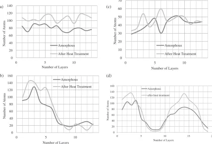
Figure 4 shows the distributions of the four-coordination atoms for the amorphous state and after the heat treatment
process, for the four specimens, Si/Ge, Si/(Ge+Cu),
(Si+Cu)/(Ge+Cu) and Si/Cu/Ge/Cu multi-layer films.
Comparing the results of (Si+Cu)/(Ge+Cu) to Si/Ge,
(Si+Cu)/(Ge+Cu) gives very low numbers of
four-coordination atoms, and no significant change in Si and
Ge layers is seen even after the heat treatment. It should be noted that the structures after heat treatment are at 1000 K.
Furthermore, we can see clearly the differences between
the results of Si/(Ge+Cu) and Si/Ge, in which when
the Cu dopants are present only in the Ge layer, the precipitation of nano-clusters decreases only in the Ge layer. This can be attributed to Cu atoms stabilizing Si and Ge in the amorphous state. In other words, Cu blocks crystallization during the heat treatment process. By placing a Cu layer at the interface between Si and Ge layers in
Si/Cu/Ge/Cu, we get a result that is just like the result
for Si/(Ge+Cu). In Fig. 4(d), at the Si and Ge layers
distinct from the Cu layer, the number of four-coordination
atoms after the annealing process increases significantly.
Unlike in (Si+Cu)/(Ge+Cu) and Ge layers in Si/
(Ge+Cu), these Cu layers do not block the precipitation
of the four-coordination atoms in both the Si and Ge layers. Moreover, it seems these Cu layers enhance the precipitation process. Interestingly, this result is very similar
to the result for the Si layer in Si/(Ge+Cu), in which
(a)
(b)
(c)
(d)
Fig. 2 Side views of the all atoms (left) and the 4 coordinated atoms (right) in the amorphous state for the four types of specimens from the [010] direction. In the left side images, Si, Ge and Cu atoms are represented as green, red and yellow circles, respectively.
(d) (a)
(b)
(c)
[image:3.595.48.300.74.497.2] [image:3.595.298.543.82.497.2]Cu dopants are present only in the Ge layer, not in the Si layer.
An actual experiment has been reported studying the role of gold (Au) in the thermoelectric properties of amorphous
Ge/Au and Si/Au thin films.11) In the experiment, four
specimens containing two different layers were prepared. Two of them had Ge and Au layers, with different thicknesses of the Au layer for each of the two specimens. The other two specimens had Si and Au layers, with different thicknesses of the Au layer for each of the two specimens. The results showed that Au enhanced the crystallization of Si and Ge. By increasing the Au composition, the crystallization was enhanced in both Si and Ge amorphous layers, and the
grain size of the thin films, i.e., the diameter of the
precipitated nano-cluster was also increased. In other words,
by controlling the structure of the Si/Ge/Au multi-layer,
the thermoelectric performance will be much improved. In our experiment, we considered that Cu will behave just like Au because both elements have similar physical and chemical characteristics according to the similarity of their
outermost electron shells. In Si/Cu/Ge/Cu, we can see that
both Si and Ge show increased precipitation of the four-coordination atoms. Thus, by placing a thin layer of Cu at
the interfaces of Si/Ge multi-layers, we can enhance the
precipitation of the four-coordination atoms and can improve the thermoelectric performance. Unfortunately, we do not have details about the distribution sizes of the nano-clusters for the present calculation or the actual Au experiment. We plan to make a detailed analysis for both computer simulations and actual experiments.
4. Conclusion
We have simulated the precipitation process in Cu-free and
Cu-added amorphous Si/Ge multilayerfilms by a molecular
dynamics method. Four specimens were prepared: Si/Ge,
Si/(Ge+Cu), (Si+Cu)/(Ge+Cu) and Si/Cu/Ge/Cu.
From the analysis of the distribution of the four-coordination
atoms before and after the heat-treatment, we clarified the
following points. (1) In the Si/(Ge+Cu) system, Ge did
not diffuse into the Si layer during annealing. (2) In the
(Si+Cu)/(Ge+Cu) system, very low numbers of
four-coordination atoms were found, and no significant change
was seen in both Si and Ge layers even after the heat treatment. We attributed this to the fact that Cu stabilized
the Si and Ge in the amorphous state. (3) In Si/Cu/Ge/Cu
system, the thin layer of Cu at the interfaces of Si/Ge
multi-layers enhanced the precipitation of the four-coordination
atoms. (4) Moreover, the Si/(Ge+Cu) system showed the
same behavior as the Si/Cu/Ge/Cu system regarding the
precipitation process at the Si layer. Therefore we believe
that precipitation of nano-clusters in Si/Ge can be controlled
by changing the amount of Cu impurity and the way that we place Cu in the system. Hence, this technique will improve thermoelectric performance in Si layer.
REFERENCES
1) A. I. Hochbaum, R. Chen, R. D. Delgado, W. Liang, E. C. Garnett, M. Najarian, A. Majumdar and P. Yang:Nature451(2008) 163.
2) F. Oki, Y. Ogawa and Y. Fujiki:Jpn. J. Appl. Phys.8(1969) 1056.
(c) (d) 0 20 40 60 80 100 120 140 160 Number of Atoms
Number of Layers Amorphous
after heat treatment
0 10 20 30 40 50 60 70
0 5 10 15 20
0 5 10
Number of
Atoms
Number of Layers Amorphous
After Heat Treatment
(a) (b) 0 20 40 60 80 100 120 140 Number of Atoms
Number of Layers Amorphous
After Heat Treatment
0 20 40 60 80 100 120 140 160
0 5 10
0 5 10
Number of
Atoms
Number of Layers Amorphous
After Heat Treatment
[image:4.595.84.512.74.365.2]3) H. Takiguchi, A. Matoba, K. Sasaki, Y. Okamoto, H. Miyazaki and J. Morimoto:Mater. Trans.51(2010) 878881.
4) H. Takiguchi, M. Aono and Y. Okamoto:Jpn. J. Appl. Phys.50(2011) 041301.
5) T. Iwasaki and H. Miura: J. Mater. Res. 16 (2001) 1789. (For the parameters of pure Si and Ge, the extended Tersoff potential used the ones proposed by Tersoff in Ref. 7).)
6) J. Tersoff:Phys. Rev. B37(1988) 6991.
7) J. Tersoff:Phys. Rev. B39(1989) 5566.
8) L. Verlet:Phys. Rev.159(1967) 98.
9) D. C. Rapaport: The Art of Molecular Dynamics Simulation, (Cambridge University Press, New York, 2004) 2nd ed., p. 49. 10) H. Takiguchi: Dissertation for Doctoral Degree, (National Defense
Academy, 2011).
![Fig. 1Side views of the initial structure of the four types of specimensfrom the [010] direction: (a) Si/Ge, (b) Si/(Ge + Cu) with Ge : Cu =6 : 4, (c) (Si + Cu)/(Ge + Cu), with 20 at% Cu in both the layers and(d) Si/Cu/Ge/Cu](https://thumb-us.123doks.com/thumbv2/123dok_us/322228.530883/2.595.57.285.66.490/side-views-initial-structure-types-specimensfrom-direction-layers.webp)
![Fig. 2Side views of the all atoms (left) and the 4 coordinated atoms (right)in the amorphous state for the four types of specimens from the [010]direction](https://thumb-us.123doks.com/thumbv2/123dok_us/322228.530883/3.595.56.551.71.502/side-views-atoms-coordinated-atoms-amorphous-specimens-direction.webp)