A SECOND-ORDER CLASS-D AUDIO AMPLIFIER∗
STEPHEN M. COX†, MENG TONG TAN‡, AND JUN YU‡
Abstract. Class-D audio amplifiers are particularly efficient, and this efficiency has led to their ubiquity in a wide range of modern electronic appliances. Their output takes the form of a high-frequency square wave whose duty cycle (ratio of on-time to off-time) is modulated at low frequency according to the audio signal. A mathematical model is developed here for a second-order class-D amplifier design (i.e., containing one second-order integrator) with negative feedback. We derive exact expressions for the dominant distortion terms, corresponding to a general audio input signal, and confirm these predictions with simulations. We also show how the observed phenomenon of “pulse skipping” arises from an instability of the analytical solution upon which the distortion calculations are based, and we provide predictions of the circumstances under which pulse skipping will take place, based on a stability analysis. These predictions are confirmed by simulations.
Key words. class-D amplifier, mathematical model, pulse skipping, total harmonic distortion
AMS subject classifications.34E10, 37N20
DOI.10.1137/100788367
1. Introduction. Class-D amplifiers are used widely in modern electronic de-vices, such as laptops, mobile phones, and hearing aids, because they are particularly efficient. Their output takes the form of a high-frequency square wave whose switching times are modulated in such a way that the low-frequency components of the output correspond to the intended audio signal. The high-frequency switching components of the output are filtered out.
For anopen-loop class-D amplifier (i.e., a class-D amplifier without feedback), it is readily shown that no distortion is introduced into the audio range of the output signal by the pulse-width modulation (PWM) process [4, 6, 12, 14]. However, due to nonidealities in practical designs (e.g., output-stage noise, component variation, or distortion in the carrier signal that drives the switching), it is desirable in practice to add a negative feedback loop to the design, but this inevitably introduces some distortion into the audio components of the output (see, for example, [15]). In this paper, we develop a mathematical model for a second-order class-D amplifier, in which a loop filter is configured as a second-order integrator. (For the purpose of our analysis, this second-order integrator is modeled as two first-order integrators connected in series.) We have previously derived similar models forfirst-order class-D amplifier designs [6], but the presentation here is more systematic and is extended to allow consideration of the stability of the analytical solutions that we develop; the question of their stability proves to be essential in explaining the observed behavior of the amplifier. A further motivation for the design considered here is that the second-order integrator is now becoming much more prevalent than its first-second-order counterpart in state-of-art audio amplifier design, as it provides higher loop gain, which allows it to better overcome the nonlinearities inherent in practical designs. Other attempts
∗Received by the editors March 11, 2010; accepted for publication (in revised form) December 6,
2010; published electronically February 22, 2011. http://www.siam.org/journals/siap/71-1/78836.html
†School of Mathematical Sciences, University of Nottingham, University Park, Nottingham NG7
2RD, United Kingdom ([email protected]).
‡School of Electrical and Electronic Engineering, Nanyang Technological University, Singapore
639798 ([email protected], [email protected]).
to model class-D amplifiers with negative feedback have generally been more ad hoc, subject to uncontrolled approximations or at least incapable of being extended beyond leading order (where this refers to a perturbation expansion in the small parameter =ωT 1,ω being a typical audio frequency and T being the period of the high-frequency carrier wave).
The second-order amplifier analyzed here exhibits somewhat richer behavior than the models we have investigated previously [6], as we now describe. We first need to note that the criterion governing the switching of the square-wave output may be interpreted geometrically as arising from the intersection of two graphs; one of these is a high-frequency triangular carrier wave. Under certain circumstances, the second-order design is observed, in both numerical simulations and circuit operation, to exhibit the phenomenon of “pulse skipping,” which generates undesirable harmonic distortion and noise on the output signal. Pulse skipping arises when the relevant graphs do not in fact intersect during a given carrier-wave period. It is not observed in the lower-order designs that we have analyzed previously [6]. We shall show that, while pulse skipping does not seem to be a feature of the analytical solution that we derive in our distortion calculation, its origin can be understood as arising from an instability of that solution.
To support our analytical description of the amplifier behavior, we carry out some complementary numerical simulations of various kinds. First, we carry out high-precision simulations of the amplifier with a formulation in terms of difference equations, using computer algebra (Maple). Next, the whole amplifier system is modeled in Simulink (i.e., the simulation tool in MATLAB) with ideal component and numerical integration blocks provided by the software model library. It will be shown in sections 4 and 5 that the mathematical model perfectly predicts the intrinsic harmonics of the amplifier (i.e., the frequency components of the output signal at multiples of the basic frequency of a sinusoidal input signal), thus capturing the main source of amplifier nonlinearity, which is particularly marked when the input signal frequency is high and its magnitude is large.
The plan of this paper is as follows. In section 2 we develop our mathematical model for the amplifier, and then in section 3 we derive a perturbation solution for that model. This perturbation solution allows us to characterize the detailed behavior of the amplifier, but a further step is needed to extract the audio-frequency content from the square-wave output of the amplifier; this step is described in section 4, and it allows us to predict the distortion introduced by the amplifier for a general input signal. Then, in section 5, we show how pulse skipping, which is not present in the solutions of section 3, can be explained by examining the stability of those solutions. We provide a criterion to be satisfied by the parameters of the problem to avoid the undesirable phenomenon of pulse skipping, and we report supporting simulations. We discuss our results and draw our conclusions in section 6.
2
+
− + +
0
v(t) −k
−c 1∫dt s(t)
g(t) p(t)
m(t)
c ∫dt
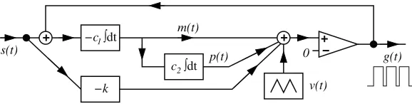
Fig. 1. Second-order class-D amplifier with negative feedback. The signals(t) is fed into a device that multiplies it by a constant −k, and also into an integrator whose output we denote by
m(t). The output of this integrator is fed into another integrator whose output we denote by p(t). The outputs of the two integrators and the multiplier are summed, together with a high-frequency triangular carrier wavev(t), and input to the noninverting input of a comparator whose inverting input is grounded. The output of the comparator is a square wave,g(t). This output is fed back to the input of the first integrator.
further added to a high-frequency triangular carrier wavev(t); this sum is fed to the noninverting input of a comparator, whose inverting input is held at zero volts. The comparator output voltage is +1 if the voltage at its noninverting input exceeds that at its inverting input, and is−1 otherwise (all voltages in this paper have been normalized by the supply voltage, assumed constant). Thus the output of the comparator is a square wave, which we denote byg(t). This square wave is fed back and added to the audio input signal to provide the full input to the first integrator.
The voltagesm(t),p(t), andh(t) satisfy
(2.1) dm
dt =−c1(s(t) +g(t)),
dp
dt =c2m(t),
with
(2.2) h(t) =m(t) +p(t).
The comparator outputg(t) satisfies
(2.3) g(t) =
+1 ifh(t)−ks(t) +v(t)>0,
−1 ifh(t)−ks(t) +v(t)<0.
The carrier wavev(t) is a triangular wave of periodT and is specified by
(2.4) v(t) =
1−4t/T for 0≤t < 12T,
−3 + 4t/T for 12T ≤t < T,
withv(t+T) =v(t) for allt. We note that in all practical implementations of such an amplifier the integration time constants in (2.1) satisfyc1T =O(1) andc2T =O(1). We denote the switching times of the output g(t) by t = An and t = Bn, for integersn, so that
(2.5) g(t) =
+1 forBn < t < An+1,
−1 forAn < t < Bn.
We further assume that the value ofg(t) switches precisely twice during each carrier-wave period, and correspondingly we write
[image:3.612.114.403.96.169.2]where
(2.7) 0< αn <12 < βn <1.
This assumption is generally the case when the amplifier is operating correctly, al-though we shall investigate below, in section 5, circumstances under whichg(t) may fail to switch precisely twice, an occurrence usually described as “pulse skipping.”
For convenience, in view of (2.1) and the need to integrate the input signal twice, we introducef(t) such that the input signal is
(2.8) s(t) =f(t).
We next integrate the ODEs (2.1) from t=An to t=An+1, to yield difference equations that relate the state of the circuit at the latter time to its state at the former.
2.1. Integration over the intervalAn < t < Bn. In this interval, it follows from (2.1), (2.5), and (2.8) that
(2.9) m(t) =−c1(f(t)−1), p(t) =c2m(t), and hence by straightforward integration we have
m(Bn) =−c1(f(Bn)−f(An)−(Bn−An)) +m(An), (2.10)
p(Bn) =−c1c2f(Bn)−f(An)−f(An)(Bn−An)−12(Bn−An)2 +c2m(An)(Bn−An) +p(An).
(2.11)
The end of this interval is when g(t) switches from −1 to +1; the corresponding switching condition is, from (2.3) and (2.4),
(2.12) m(Bn) +p(Bn)−ks(Bn)−3 + 4βn= 0.
2.2. Integration over the interval Bn < t < An+1. In this interval, it follows from (2.1), (2.5), and (2.8) that
(2.13) m(t) =−c1(f(t) + 1), p(t) =c2m(t),
and hence, by integration over this interval and use of (2.10) and (2.11), we have
m(An+1) =−c1(f(An+1)−f(An) +An+1+An−2Bn) +m(An), (2.14)
p(An+1) =−c1c2f(An+1)−f(An)−f(An)(An+1−An) +12(An+1+An−2Bn)2−(Bn−An)2 +c2m(An)(An+1−An) +p(An). (2.15)
The switching condition at the end of this interval is then, from (2.3) and (2.4),
(2.16) m(An+1) +p(An+1)−ks(An+1) + 1−4αn+1= 0.
2.3. Summary. The typical behavior of the various voltages in the circuit is illustrated in Figure 2.
-1 -0.5 0 0.5 1
nT A
nB
n(n+1)T
t
h
v
g
m
p
Fig. 2.Typical behavior of the voltages in the circuit. For the purposes of illustration, we have takenc1T = 1.5,c2T = 4,k= 0,s= 0.4(constant input signal).
3. Solving the model. In operation, a class-D amplifier has carrier-wave fre-quency much greater than a typical audio frefre-quency. Thus if ω is a typical audio frequency (corresponding to an inputs(t) =s0sinωt, for instance) then
(3.1) ≡ωT 1.
We thus use the small parameter as the basis for a perturbation expansion of the problem.
We introduce the dimensionless time variable
(3.2) τ=ωt=t/T.
Then, sinces(t) has typical frequencyω, we may write
(3.3) s(t) =S(τ).
If we also introduceF(τ) such that
(3.4) S(τ) =d
2F(τ)
dτ2 ,
it follows that
(3.5) F(τ) =
2
T2f(t).
Next we note that, although the voltages in the amplifier circuit vary on the fast time scale of the carrier wave, theαnandβnthemselves vary only on the slower audio time scale. Thus we introduce functionsA,B,M, andP such that
(3.6) A(n) =αn, B(n) =βn, M(n) =m(An), P(n) =p(An)
[image:5.612.145.366.102.213.2]B,M, and P:
0 =−c1T−1(F2−F1)−( ¯B−A)¯ + ¯M
−c1c2T2−2(F
2−F1)−−1( ¯B−A)F¯ 1−1 2( ¯B−
¯ A)2
+c2T( ¯B−A) ¯¯ M+ ¯P−3 + 4 ¯B−kS2, (3.7)
M((n+ 1)) =−c1T−1(F3−F1) + 1 +A((n+ 1)) + ¯A−2 ¯B + ¯M, (3.8)
P((n+ 1)) =−c1c2T2
−2(F
3−F1)−−1(1 +A((n+ 1))−A)F¯ 1
+1
2(1 +A((n+ 1)) + ¯A−2 ¯B)
2−( ¯B−A)¯ 2
+c2T(1 +A((n+ 1))−A) ¯¯ M + ¯P , (3.9)
0 =M((n+ 1)) +P((n+ 1)) + 1−4A((n+ 1))−kS3. (3.10)
In all of these expressions, and in similar expressions to follow, we use the prime in the obvious way, so thatF(τ) denotes dF(τ)/dτ. The subscripts onF,F, andS are used for brevity to indicate the arguments of these functions: F1=F((n+A(n))), F2=F((n+B(n))), F3 =F((n+ 1 +A((n+ 1)))), S2 =S((n+B(n))), and S3 =S((n+ 1 +A((n+ 1)))). To aid clarity, we have written ¯A to mean A(n), with corresponding definitions for ¯B, ¯M, and ¯P.
These four equations are simply a restatement of the corresponding set of dif-ference equations (2.12), (2.14), (2.15), and (2.16) (with (2.10) and (2.11)). Next, although only the sampled values of A, B, M, and P are physically relevant, ac-cording to (3.6), we suppose that these four functions are smoothly interpolated to intervening times, and that (3.7)–(3.10) in fact hold not just at τ = n, but at all intermediate times too. Thus we aim to solve
0 =−c1T−1[F(τ+B(τ))−F(τ+A(τ))]−[B(τ)−A(τ)]+M(τ)
−c1c2T2−2[F(τ+B(τ))−F(τ+A(τ))]
−−1F(τ+A(τ))(B(τ)−A(τ))−1
2(B(τ)−A(τ))
2
+c2T(B(τ)−A(τ))M(τ) +P(τ)−3 + 4B(τ)−kS(τ+B(τ)), (3.11)
M(τ+) =−c1T−1[F(τ++A(τ+))−F(τ+A(τ))] + 1 +A(τ+) +A(τ)−2B(τ)+M(τ),
(3.12)
P(τ+) =−c1c2T2
−2[F(τ++A(τ+))−F(τ+A(τ))]
−−1F(τ+A(τ))(A(τ+)−A(τ))
+1
2(1 +A(τ+) +A(τ)−2B(τ))−(B(τ)−A(τ))
2
+c2T(A(τ+)−A(τ))M(τ) +P(τ), (3.13)
0 =M(τ+) +P(τ+) + 1−4A(τ+)−kS(τ++A(τ+)). (3.14)
andP. An exact solution of these equations seems infeasible; hence we solve them by first expanding the unknown functions as series in, so that
(3.15) A(τ) =
∞
n=0
nA(n)(τ),
with similar representations forB,M, andP, and then solving the resulting equations at successive orders in.
3.1. Solution for the functionsA,B,M, andP. The expansion in powers of is rather lengthy and involved, and is carried out using computer algebra. Fur-thermore, since an additional calculation must subsequently be performed to provide details of the audio output of the amplifier, we give only the leading-order results here forA,B,M, andP. These are that
A(0)(τ) = 1
16(1−S(τ))(4−c1T(1 +S(τ))),
(3.16)
B(0)(τ) = 1
2+161(1 +S(τ))(4−c1T(1−S(τ))),
(3.17)
M(0)(τ) =−1
4c1T(1−S2(τ)),
(3.18)
P(0)(τ) =−(1−k)S(τ).
(3.19)
The results for A(0) and B(0) in particular turn out to be the same as for other negative-feedback class-D amplifier designs that we have considered [6] (although the terms at higher orders in differ). Thus, in view of (3.6), the switching times are determined by
αn =161(1−s(nT))(4−c1T(1 +s(nT))) +O(), (3.20)
βn =12+161(1 +s(nT))(4−c1T(1−s(nT))) +O(), (3.21)
and hence during thenth carrier-wave period the average value of the outputg(t) is
(3.22) (+1)×αn+ (−1)×(βn−αn) + (+1)×(1−βn) =−s(nT),
so that in the audio-frequency range, the output is, to leading order in, simply−s(t). The minus sign is of no consequence in the context of an audio amplifier, and so to
leading order in the present design is confirmed to introduce no audio distortion.
There is, unfortunately, distortion at higher orders in, as we shall see.
4. Determining the audio output of the amplifier. Once the problem (3.11)–(3.14) has been solved to some order in , it remains to calculate the audio output corresponding to a given audio input, assuming that all the high-frequency con-tributions to the output, associated with switching around the carrier-wave frequency, have been filtered out. Such a calculation is generally performed in the engineering lit-erature (for a wide variety of switching technologies, not just class-D amplifiers) using Black’s method [4, 9]. However, Black’s method is rather algebraically cumbersome, as are some alternatives [13, 14], and will not be used here.
Instead, to calculate the audio output of the amplifier, we follow a compact for-mulation, which we have recently introduced elsewhere [5, 7] in the context of power converters. Thus we begin by noting that the full amplifier output may be written in the form
(4.1) g(t) = ∞
n=−∞
ψ(t;Bn, An+1)−ψ(t;An, Bn)
whereψ is the “top-hat” function given by
(4.2) ψ(t;t1, t2) =
1 fort1< t < t2, 0 otherwise.
Hence the Fourier transform of the output is
ˆ g(ω) =
∞
−∞
e−iωtg(t) dt
= 2(−iω)−1 ∞
n=−∞
e−iω(n+αn)T −e−iω(n+βn)T
= 2(−iω)−1 ∞
n=−∞ e−iωnT
e−iωA(n)T −e−iωB(n)T
. (4.3)
Note that this formula clearly cannot be used directly to evaluate ˆg(0), so later we shall have to consider the zero-frequency component ofg(t) separately. We next apply the Poisson resummation identity,
(4.4)
∞
n=−∞ Φ(n) =
∞
n=−∞
∞
−∞
e2πinφΦ(φ) dφ,
to (4.3), which yields
(4.5) g(ω) = 2(ˆ −iω)−1
∞
−∞ e−iωφT
∞
n=−∞ e2πinφ
e−iωA(φ)T −e−iωB(φ)T
dφ.
The integral in this expression is in the form of a Fourier transform, with each term in the sum corresponding to frequencies around thenth harmonic of the carrier-wave frequency. If our concern is the audio part of the output, which we shall denote by ga(t), then only the term withn= 0 is of interest. Thus we see thatga(t) has Fourier transform
(4.6) gˆa(ω) = 2(−iω)−1
∞
−∞ e−iωφT
e−iωA(φ)T −e−iωB(φ)T
dφ.
By expanding each of the exponentials in this expression as a Taylor series, and using the result
(4.7)
∞
−∞
(−iω)e−iωφTΦ(φ) dφ=−T−1
∞
−∞
e−iωφTΦ(φ) dφ,
we see that
ˆ
ga(ω) = 2
∞
−∞ e−iωφT
∞
n=1
(−1)n−1T n!
dn−1
dφn−1 [An(φ)−Bn(φ)] dφ
= 2
∞
−∞ e−iωt
∞
n=1
(−1)n−1T
n−1
n! dn−1
dtn−1[An(t/T)−Bn(t/T)] dt.
(4.8)
zero. Hence
ga(t) = 1 + 2∞
n=1
(−1)n−1T
n−1
n! dn−1
dtn−1[An(t/T)−Bn(t/T)]
= 1 + 2 ∞
n=1
(−1)n−1
n−1
n! dn−1
dτn−1[An(τ)−Bn(τ)]
= 1 + 2(A(τ)−B(τ))− d dτ
A2(τ)−B2(τ) +2
3 d2 dτ2
A3(τ)−B3(τ) +· · ·.
(4.9)
Finally, by substituting the solutions obtained previously forA and B (see sec-tion 3.1) in (4.9), after lengthy algebra we find the audio output to be
(4.10)
ga(t) =−S(τ) + 2 24c1c2T2
d2 dτ2
24(1−k) +c1c2T2 S(τ)−c1c2T2S3(τ)
+O(3),
where we recall thatτ =ωt. Several features of this result are worthy of note. First, in view of (3.3), the dominant contribution to the audio output is (minus) the input signal, with no distortion. Second, there is no distortion atO(). Third, the distortion at O(2) comprises terms linear and cubic in the input signal. So, for a sinusoidal input signal, the output, to the order calculated in (4.10), comprises the fundamental and its third harmonic: for example, ifs(t) =s0sinωt, then
ga(t) =−s0sinωt+ ω
2
96c1c2
−(96(1−k) + 4c1c2T2)s0+ 3c1c2T2s30 sinωt
−9c1c2T2s3 0sin 3ωt
+· · · . (4.11)
The results above enable us to give an analytical expression for the total harmonic distortion (THD) of the amplifier, defined as follows. If a sine wave
(4.12) s(t) =s0sinωt
is the input and if
(4.13) ga(t) = ∞
n=−∞ gneniωt
is the audio output, then the THD is defined as
(4.14) THD =
|g2|2+|g3|2+· · · |g1| .
In the second-order amplifier analyzed above, the THD based on (4.11), toO(2), is
(4.15) THD∼323ω2T2s20.
We have carried out various comparisons between this result and simulations based on the Simulink model of the class-D amplifier; two of these are reported below. The parameter values used for comparisons are
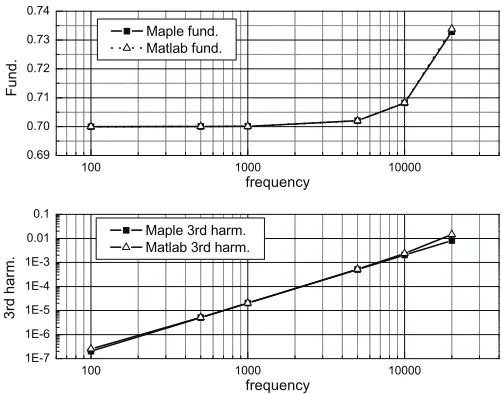
Fig. 3. Top: fundamental component of the PWM output signal, |g1|, plotted against input signal frequency in Hz, i.e.,ω/(2π). Bottom: third harmonic component of the PWM output signal,
|g3|, plotted against the input signal frequency in Hz, i.e., ω/(2π). In each case, s(t)is given by
(4.12), withs0= 0.7, and the comparison is made between an analytical solution (from Maple) and
a simulation (from MATLAB).
Thus the carrier wave has frequency 250kHz. The values of the integrator coefficients, c1 andc2, have been chosen to be typical of practical designs.
In the first comparison, the input signal magnitude s0 is fixed at 0.7 and its frequency is varied between 100Hz and 20kHz. The analytical result (4.11) and sim-ulation results are shown in Figure 3. The figure shows that the analytical results match the simulations extremely well, in the middle frequency range. At high fre-quency (above approximately 10kHz), the analytical prediction for the third harmonic is noticeably below the simulation results. Of course, it should be borne in mind that when the input signal frequency is above 7kHz, its third harmonic is out of the audio range (i.e., from 20Hz to 20kHz). Therefore, the small mismatch is acceptable. Note that when the input signal frequency is 100Hz, the simulation result for the third harmonic is a little bit higher than the analytical result. It turns out that this is due to the effect ofpulse skipping, which will be discussed in the next section.
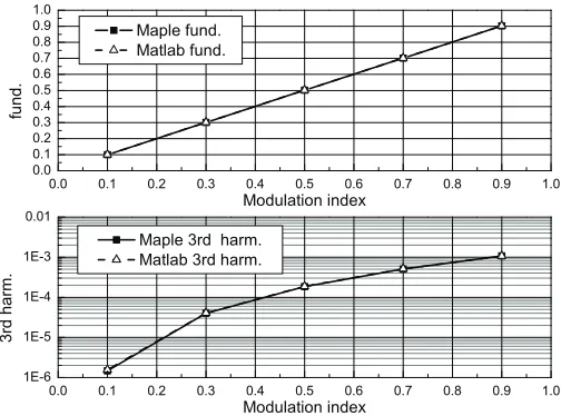
In the second comparison, the input signal frequency is fixed at 5000Hz and the input signal magnitude (termed themodulation index in the engineering literature) varies from 0.1 to 0.9, in increments of 0.2. The analytical and simulation results are shown in Figure 4. Again, there is excellent agreement between the two.
[image:10.612.125.376.101.298.2]Fig. 4. Top: fundamental component of the PWM output signal, |g1|, plotted against the
modulation index, i.e., input signal magnitude, s0. Bottom: third harmonic component of the
PWM output signal,|g3|, plotted against the modulation index. In each case,s(t)is given by(4.12),
with frequency5kHz (i.e.,ω= 2π×5000), and the comparison is made between an analytical solution (from Maple) and a simulation (from MATLAB).
Indeed, during the numerical simulations discussed at the end of the previous section, pulse skipping is found to occur shortly after each positive and negative peak ins(t). Such pulse skipping raises the noise floor of the output signal and causes significant harmonic distortion. For these reasons, it is an undesirable phenomenon, because it limits the performance of the amplifier, particularly when the input signal is of relatively low frequency and large magnitude.
Pulse skipping manifests itself in our mathematical model when the solution to (2.12) or (2.16) is required to fall outside of its intended range, that is, if the solution is required to satisfy αn > 12 or βn > 1. Intriguingly, accurate numerical iteration of the difference equations (2.12), (2.14), (2.15), and (2.16), for the same parameters as used in the numerical integrations, shows no evidence of pulse skipping, and we find thatαn andβn remain comfortably within their designated constraints, as given by (2.7). Furthermore, in the continuous description of section 3, pulse skipping would be indicated if the functionsA and B were to venture into the range A > 12 or B > 1. However, it is clear from (3.16) and (3.17) that if the signal remains within the bounds −1 < s(t) < 1 and if c1T < 2 (which is the case in practical applications), then, based on the leading-order contributionsA∼A(0) andB∼B(0), neither of the transgressions A > 12 and B > 1 may occur. (Of course, we should note that, while A > 12 or B > 1 would indicate the possibility of pulse skipping, the continuous model is unable to predict in detail the behavior of the system during pulse skipping, because its underlying assumption of slow, smooth variations inA(τ) and B(τ) specifically precludes investigation of such fast instabilities; see [2, 8].) A little further analysis, in the case s(t) = s0sinωt, near the maxima and minima of s(t), shows that if higher-order terms are retained inA and B, then we may indeed find A > 12 or B > 1, but only if the amplitude s0 is very close to 1—in fact, if
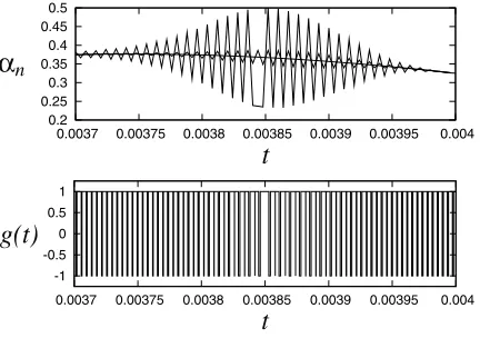
[image:11.612.127.379.102.289.2]0.2 0.25 0.3 0.35 0.4 0.45 0.5
0.0037 0.00375 0.0038 0.00385 0.0039 0.00395 0.004
α
nt
-1 -0.5 0 0.5 1
0.0037 0.00375 0.0038 0.00385 0.0039 0.00395 0.004
g(t)
t
Fig. 5. Top: plot of the switching constant αn≡(AnmodT)/T against timest=nT. Only the discrete points (nT, αn) have any physical meaning; they are joined by lines to aid the eye. The smooth curve is the result of numerical iteration of the difference equations (2.12), (2.14), (2.15), and(2.16)in the computer algebra package Maple using24digits of numerical precision; the other solutions are computed with11and10digits of precision (respectively, resulting in successively stronger evidence of instability). Parameter values are as in(4.16), and the input signal is0.7 cosωt, with frequency 400Hz. With 10digits of precision, a pulse is skipped during the switching period beginning att= 0.003844. Bottom: corresponding plot ofg(t), showing the skipped pulse.
reported above, since it occurs for an input signal of far more modest amplitude (for example,s0 = 0.7, with2= (ωT)2= 0.016). So there is an apparent inconsistency between the theory and (numerical and actual) experiments regarding the presence or absence of pulse skipping.
A resolution can be found by considering thestability of the analytical solution that we have evaluated using high-precision computer-algebra simulations of the differ-ence equations. A crude way to investigate the stability of this solution is by reducing the precision with which these calculations are performed. At very high precision (for example, 24 digits of precision in Maple), we find that, for the cases(t) =s0sinωt, withs0= 0.7 and frequency 400Hz, perturbations to the exact solution forαn orβn induced by numerical roundoff error generally do not grow to any significant mag-nitude (hence, it is possible to compute this solution accurately using high-precision arithmetic). However, if we use lower-precision arithmetic, then the roundoff errors are greater, and we observe that, near the maxima and minima ofs(t), these roundoff errors do grow, in an oscillatory fashion. Eventually, if the precision is low enough, these perturbations may become sufficiently large that they cause pulse skipping; see Figure 5. Since the numerical integrations all necessarily have much lower accuracy than our numerical iterations of the difference equations, this explains why pulse skip-ping is seen there. The noise present in the circuit implementations of this amplifier is also evidently sufficiently great to trigger pulse skipping. Note that when pulse skipping occurs in simulations of our difference equations, we need to broaden the definition ofαn andβn so that
(5.1) αn= An modT
T , βn=
BnmodT
T .
[image:12.612.153.369.100.252.2]cannot be captured by the analysis of section 3, which accommodates only variations on the audio time scale. We thus turn next to an analysis of the difference equations (2.12), (2.14), (2.15), and (2.16).
5.1. Instability. For notational convenience we now denote m(An) bymn and p(An) bypn. We shall refer to the solution obtained by solving the difference equa-tions in high-precision arithmetic, with no fast perturbaequa-tions, as the “unperturbed solution.” We let the unperturbed solution be denoted by
(5.2) m(An) = ¯mn, p(An) = ¯pn, An= ¯An, Bn = ¯Bn.
The perturbed solution is then written as
(5.3) mn = ¯mn+δmn, pn= ¯pn+δpn, An= ¯An+δAn, Bn= ¯Bn+δBn.
We suppose that an initial perturbation is induced by roundoff error, and we ex-plore whether such a perturbation decays or grows, that is, whether the unperturbed solution is stable or unstable.
The governing difference equations may be written compactly as follows. The equation governing the switching timet=An is essentially (2.16), which we write as
(5.4) φ0(mn, An) =pn.
The equation governing the switching timet=Bn is (2.12), which we write as
(5.5) φ1(mn, pn, An, Bn) = 0.
The equations determiningmn+1 andpn+1, from (2.14) and (2.15), respectively, may be written in the form
(5.6) φ2(mn, An, An+1, Bn) =mn+1, φ3(mn, pn, An, An+1, Bn) =pn+1.
Finally, (2.16) for the switching timet=An+1 may be written as
(5.7) φ4(mn+1, An+1) =pn+1.
We next linearize each of these equations about the unperturbed solution. Thus from (5.4) and (5.5) we obtain
(5.8) ∂φ0 ∂mnδmn+
∂φ0
∂AnδAn=δpn,
∂φ1 ∂mnδmn+
∂φ1 ∂pnδpn+
∂φ1 ∂AnδAn+
∂φ1
∂BnδBn = 0,
which we may use to determineδpnandδBnin terms ofδmnandδAn. The remaining equations, (5.6) and (5.7), give us
∂φ2 ∂mnδmn+
∂φ2 ∂AnδAn+
∂φ2
∂An+1δAn+1+ ∂φ2
∂BnδBn =δmn+1, (5.9)
∂φ3 ∂mnδmn+
∂φ3 ∂pnδpn+
∂φ3 ∂AnδAn+
∂φ3
∂An+1δAn+1+ ∂φ3
∂BnδBn =δpn+1, (5.10)
∂φ4
∂mn+1δmn+1+ ∂φ4
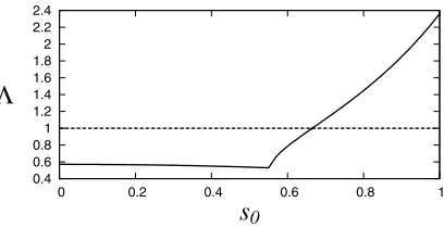
0.4 0.6 0.8 1 1.2 1.4 1.6 1.8 2 2.2 2.4
0 0.2 0.4 0.6 0.8 1
Λ
s
0Fig. 6.Plot ofΛ≡max(|λ|,|μ|)againsts0, for a constant input signals(t)≡s0, and for the parameter values in (4.16). The analytical solution, based on (3.16)–(3.19), is stable whereΛ<1 and unstable where Λ>1. We find that where Λ>1, the eigenvalue responsible for instability is real and negative, consistent with the oscillations seen in the values ofαnshown in Figure 5.
Using (5.11), we may then eliminate δpn+1, leaving a pair of equations relating (mn+1, An+1) to (mn, An), which we may write in the form
(5.12)
mn+1 An+1
=Cn
mn An
,
where Cn is a 2×2 matrix, whose coefficients may be computed numerically, simul-taneously with the numerical iteration of the solution itself.
Now, since the governing system is nonautonomous (it is forced by the time-dependent input signal), the stability of perturbations in general requires careful con-sideration. Here, however, the input signal varies only slightly during a carrier-wave period, so thatCn+1−Cn=O(), and hence the eigenvaluesλn andμnof the matrix Cngive a good indication of the stability or otherwise of the unperturbed solution. If Λ≡max(|λn|,|μn|)>1, then there is instability.
Figure 6 shows the values of Λ corresponding to the analytical solution resulting from a constant input signal s(t) ≡ s0, for values of s0 in the range 0 ≤ s0 ≤ 1 (by symmetry the values of Λ are the same for s0 → −s0). Here, the problem is autonomous, and all the matricesCn are equal. The parameter values used are given in (4.16). We see that for small and moderate values ofs0 the analytical solution is stable, since Λ <1. Furthermore, for the smallest values of s0, the two eigenvalues λ, μare complex conjugates; for larger values ofs0 (above approximately 0.55), each of the eigenvalues is real and negative. For s0 > sc, where sc ≈0.665, Λ > 1 and the solution is unstable. We have confirmed this threshold between stability and instability by carrying out numerical simulations for a constant input signal; we find excellent agreement with the instability thresholdsc.
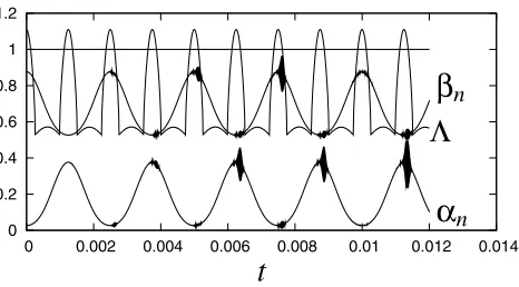
Figure 7 shows the growth of perturbations to the switching times, for a sinusoidal input signal with peak amplitude 0.7 in simulations of our difference equations (2.12), (2.14), (2.15), and (2.16), using 10 digits of precision. Since, as shown in Figure 6, the smooth solution for the response of the amplifier is unstable when s(t)> sc, it is clear that we expect growth of perturbations around the maxima in the absolute value of s(t). Furthermore, it is also clear that the corresponding high-frequency disturbances will tend to become visible towards the later parts of the interval of instability, since they must grow from a small initial amplitude (roundoff error in these simulations). These considerations are consistent with the observations of pulse skipping in numerical simulations and in circuit implementations of the amplifier.
[image:14.612.156.360.99.204.2]0 0.2 0.4 0.6 0.8 1 1.2
0 0.002 0.004 0.006 0.008 0.01 0.012 0.014
t
α
nβ
nΛ
Fig. 7. Plots for an input signals(t) =s0cosωtand for the parameter values in (4.16), with
s0= 0.7and frequency 400Hz. Upper curve shows Λ≡max(|λn|,|μn|)against time; where Λ>1, we expect disturbances to the exact solution to grow. Middle and lower curves showβn and αn, respectively. The appearance of high-frequency perturbations to the smooth solutions forβnandαn
can clearly be seen, corresponding to the time intervals whereΛ>1. Simulations are of the difference equations(2.12),(2.14),(2.15), and(2.16), using10digits of precision in calculations.
onset of oscillations as|s(t)|passes through the thresholdsc, using the techniques of Baer, Erneux, and Rinzel [1]. In our context, their WKB-type analysis would provide a quantitative estimate of the delay between the passage of |s(t)| through sc and the visible manifestation of instability. Furthermore, it is conceivable that such an analysis could be extended to provide information about the effects of the instability on the output spectrum. However, we shall not embark on such a detailed analysis here, because the primary engineering interest is in the behavior of the amplifier prior to the onset of the high-frequency instability, and certainly prior to the onset of pulse skipping.
5.2. General stability criteria. We now turn to the determination of condi-tions under which the amplifier may suffer an instability, potentially leading to pulse skipping. Although it seems infeasible to give such conditions for a general input signal, we shall proceed with the simpler task of approximating the appropriate con-ditions for a typical audio input, by considering in more detail the stability of the amplifier output for a constant input signal. Our goal is to determine analytical conditions on the parameters to preclude pulse skipping.
For the case of a constant input signal, s = s0, we consider the eigenvalues of the matrix in (5.12) (recall that in the steady-state operation of the amplifier for a constant input signal, all the matricesCn are identical). These eigenvalues satisfy a quadratic characteristic equation, whose coefficients are complicated functions of the parameterss0,c1,c2, andT; these complicated expressions are not recorded here. It is readily determined from this characteristic equation (although algebraically involved to do so) that instability with an eigenvalueλpassing through the unit circle at eiθ is possible only if θ =π; i.e., a transition to instability is possible only as λpasses through the value−1. This result helps significantly in the analysis that follows.
If we now fixc1,c2, andT and seek conditions on the input amplitudes0at which instability arises, we obtain the quartic equation
(5.13) 4c2
1c22T4s40−8c1T(c1c22T3+16c2T+8c1T)s20+1024+64c21T2+4c21c22T4−128c1c2T2= 0.
[image:15.612.152.385.99.228.2]impractical. This assumption is equivalent to requiring the condition
(5.14) 1024 + 64c21T2+ 4c21c22T4−128c1c2T2>0.
Equation (5.13) is then readily observed to have two positive roots for s20, and we denote the corresponding positive roots for s0 by s−0 and s+0 (with s+0 > s−0). The amplifier would then be stable for constant inputs with 0≤ |s0|< s−0 and unstable for s−
0 <|s0|. However, the input signal amplitude is limited to be no greater than 1, so
if we can ensure thats−0 >1, then the amplifier will be stable for all allowed inputs. Analysis of (5.13) shows thats−0 >1 provided
(5.15) c1c2T2<4.
This is the condition for pulse skipping to be entirely precluded. If it is not satisfied, then the smaller positive root of (5.13) gives the threshold value of the input signal at which instability arises, potentially leading to pulse skipping. Numerical simulations of the amplifier confirm these thresholds.
Of course, the analysis above concerns a constant input signal. For a more general audio input signal, we do not expect to see pulse skipping if the condition (5.15) is satisfied. However, if insteadc1c2T2>4, then there is the potential for pulse skipping whenevers(t) exceeds the thresholds−0 given by (5.13). But there must be adequate time for any noise to grow to an appreciable level whiles(t)> s−0, so pulse skipping will be more prevalent forlow-frequencyaudio inputs of a given amplitude (as observed in practice). Unfortunately, it is beyond the scope of our analysis to give exact formulas for this frequency dependence.
6. Conclusions. We have developed a mathematical model for a second-order class-D amplifier with negative feedback, and we used it to derive an exact mathemat-ical expression for the most significant (third-harmonic) distortion term. A correct, predictive determination of this distortion term has not previously been possible. The analytical prediction is in excellent agreement with spectra obtained from numerical simulations.
We have shown how the pulse skipping that is observed in practice (in both nu-merical simulations and in circuit implementations of the amplifier) arises from an instability of the analytical solutions we have derived for the circuit behavior. By an-alyzing the stability of our smooth analytical solution, we have show that we expect instability when the input signal exceeds some threshold amplitude. This result is con-sistent with observations of associated pulse skipping around (but generally slightly after) maxima and minima of the input signal, once the instability has had the oppor-tunity to grow to an appreciable magnitude. Pulse skipping generates high-frequency noise, which is filtered out along with the high-frequency components associated with the switching. It is also responsible for the slight disagreements observed, with low-frequency inputs, between analytical predictions of the output audio spectrum which ignore the phenomenon and simulations which necessarily suffer from it.
In the future, we hope to develop this model to explore ways in which the most significant distortion term can be eliminated, although this is not a simple task.
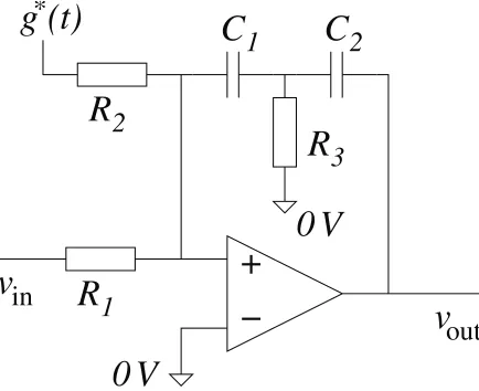
Appendix A. Relation between integration time constants and system parameters. In practice, the integrators in the amplifier are implemented by means
of a second-order loop filter, as shown in Figure 8. In this appendix, we record
+
out
0 V
R
1
R
2
0 V
R
3
g (t)
*
C
1
C
2
−
v
in
v
Fig. 8.Circuit schematic of the second-order loop filter used to implement the two integrators of the amplifier design.
All quantities in Figure 8 are assumed to be dimensional, so that
vin(t) =K1s(t), g∗(t) =K
2g(t), vout(t) =K3(m(t) +p(t))
for some voltage scaling factorsK1,K2, andK3. Then it is readily determined that, in between the switching times ofg∗(t),vout(t) satisfies the second-order differential equation
v
out(t) =−
C1+C2 C1C2R1vin −
1 C2R3
1 C1R1vin+
1 C1R2g∗(t)
.
Hence
c1=(C1+C2)K2
C1C2R2K3 , c2= 1 (C1+C2)R3.
REFERENCES
[1] S. M. Baer, T. Erneux, and J. Rinzel,The slow passage through a Hopf bifurcation: Delay, memory effects, and resonance, SIAM J. Appl. Math., 49 (1989), pp. 55–71.
[2] S. Banerjee and G. C. Verghese,Nonlinear Phenomena in Power Electronics: Bifurcations, Chaos, Control and Applications, Wiley–IEEE Press, New York, 2001.
[3] M. Berkhout and L. Dooper,Class-D audio amplifiers in mobile applications, IEEE Trans.
Circuits Syst. I Regul. Pap., 57 (2010), pp. 992–1002. [4] H. S. Black,Modulation Theory, Van Nostrand, New York, 1953.
[5] S. M. Cox,Voltage and current spectra for a single-phase voltage-source inverter, IMA J.
Appl. Math., 74 (2009), pp. 782–805.
[6] S. M. Cox and B. H. Candy,Class-D audio amplifiers with negative feedback, SIAM J. Appl.
Math., 66 (2005), pp. 468–488.
[7] S. M. Cox and S. C. Creagh,Voltage and current spectra for matrix power converters, SIAM
J. Appl. Math., 69 (2009), pp. 1415–1437.
[8] M. di Bernardo, C. J. Budd, A. R. Champneys, and P. Kowalczyk,Piecewise-Smooth Dynamical Systems: Theory and Applications, Springer, London, 2008.
[9] D. G. Holmes and T. A. Lipo,Pulse Width Modulation for Power Converters, IEEE Press,
[image:17.612.148.365.96.273.2][10] S. K. Mazumder, A. H. Nayfeh, and D. Boroyevich,Theoretical and experimental investi-gation of the fast- and slow-scale instabilities of a DC–DC converter, IEEE Trans. Power Electronics, 16 (2001), pp. 201–216.
[11] S. K. Mazumder, A. H. Nayfeh, and D. Boroyevich,An investigation into the fast- and slow-scale instabilities of single phase bidirectional boost converter, IEEE Trans. Power Electronics, 18 (2003), pp. 1063–1069.
[12] P. H. Mellor, S. P. Leigh, and B. M. G. Cheetham,Reduction of spectral distortion in class D amplifiers by an enhanced pulse width modulation sampling process, IEE Proc. G, 138 (1991), pp. 441–448.
[13] C. Pascual, Z. Song, P. T. Krein, D. V. Sarwate, P. Midya, and W. J. Roeckner, High-fidelity PWM inverter for digital audio amplification: Spectral analysis, real-time DSP implementation, and results, IEEE Trans. Power Electronics, 18 (2003), pp. 473–485. [14] Z. Song and D. V. Sarwate,The frequency spectrum of pulse width modulated signals, Signal
Process., 83 (2003), pp. 2227–2258.
[15] M. T. Tan, J. S. Chang, H. C. Chua, and B. H. Gwee,An investigation into the parame-ters affecting total harmonic distortion in low-voltage low-power class-D amplifiers, IEEE Trans. Circuits Syst. I Regul. Pap., 50 (2003), pp. 1304–1315.
[16] C. K. Tse,Complex Behavior of Switching Power Converters, CRC Press, Boca Raton, FL,