1 This paper is a postprint of a paper submitted to and accepted for publication in IET Power Electronics and is subject to Institution of Engineering and Technology Copyright. The copy of record is available at IET Digital Library
Hybrid HVDC Circuit Breaker with Self-Powered Gate Drives
Francis B. Effah 1, Alan J. Watson 1*, Chao Ji 1, Emmanuel Amankwah 1, C. Mark Johnson 1, Colin Davidson 2, Jon Clare 1
1
Department of Electrical and Electronic Engineering, The University of Nottingham, NG7 2RD, Nottingham, UK
2
Alstom Grid, Stafford, ST17 4UJ *
alan.watson@nottingham.ac.uk
Abstract: The ever increasing electric power demand and the advent of renewable energy sources have revived the interest in high-voltage direct current (HVDC) multi-terminal networks. However, the absence of a suitable circuit breaker or fault tolerant VSC station topologies with the required characteristics (such as operating speed) have, until recently, been an obstacle in the development of large scale multi-terminal networks for HVDC. This paper presents a hybrid HVDC circuit breaker concept which is capable of meeting the requirements of HVDC networks. Simulation results are presented which are validated by experimental results taken from a 2.5kV, 700A rated laboratory prototype.
1. Introduction
2
Compared with AC networks, DC current interruption is inherently difficult, mainly due to the absence of a natural current zero crossing in DC systems. Furthermore, DC circuit breakers are required to clear a fault very quickly, typically within a few milliseconds, and to dissipate the large amount of energy which is stored in the system inductances [5]. Commercially existing high voltage DC switches have operating times of several tens of milliseconds, which although suitable for load current switching, is too slow for clearing faults to meet the needs of a reliable HVDC network [12]. Therefore, new technologies for fast and reliable HVDC circuit breakers are required.
A purely solid-state circuit breaker for HVDC networks was proposed and patented in 1997 [13]. Although a very fast response time can be achieved, this arrangement cannot be considered as a practical solution, due to the high steady-state losses which are dissipated in the high voltage switching branch. In 2011, a hybrid circuit breaker solution was demonstrated at CIGRE, Bologna [12]. This topology can be considered as an updated version of that considered in [13], i.e. a low voltage (LV) branch consisting of ultra-fast mechanical switch and an insulated gate bipolar transistor (IGBT) is introduced to carry the nominal current and thus avoid the high steady-state losses. The solution presented however, does not have self- powered gate drives for the auxiliary arm. This would be advantageous since powering such circuits in HVDC systems is a well-known challenge. Other solutions have also been proposed in this highly active research area [14-17].
This paper presents an alternative hybrid HVDC circuit breaker topology based on [16]. This topology has a fast response time, thus enabling its use with state of the art switching hardware and furthermore it utilises self-powered gate drives in the high voltage branch, thus eliminating the need for external gate power supplies for the circuit breaker.
3
2. Principles of hybrid circuit breakers
A circuit breaker (CB) is required to accomplish the following basic requirements: 1) large current handling capability without excessive losses; 2) capability of very fast transition from the conducting to the blocking state in case of a fault, without damaging itself in the process; and 3) after current interruption, when it is open, the dielectric strength must be built up in order to block any current despite the high potentials at the terminals [18-24]. Traditional mechanical circuit breakers (MCBs) have a very small contact resistance in the closed position, with galvanic separation in the open state. However, they have a long reaction time due to the need to extinguish the fault in an arc chute [18-22].
Solid–state circuit breakers (SSCBs), based on high-power semiconductors, offer many advantages when compared to conventional solutions. In SSCBs, due to the absence of moving parts, there is no arcing, contact erosion, or bounce. SSCBs are therefore faster, minimizing fault duration. However, because of the semiconductor’s on-state resistance resulting in heating and power loss, the SSCBs fail as far as the first basic requirement of a CB mentioned above is concerned.
4 Fig.1a.DC hybrid circuit breaker Fig.1b.The proposed hybrid HVDC circuit breaker concept
Fig.1c.Detailed structure of unidirectional main branch Fig.1d. Snubber circuit and surge arrester branch
The normal current flows through the main contact for low power dissipation. The semiconductor device connected in parallel to the main contact operates after a fault occurrence and performs the fault current interruption. It is to be noted that as the semiconductor device is turned off to finally clear the fault, the voltage across it rises due to the stored energy in the line inductance. This voltage may reach a very high value and destroy the hybrid circuit breaker if no additional components are used for reducing the voltage. As shown in Fig. 1a, an overvoltage protection device is connected in parallel to the semiconductor device to reduce the peak voltage. Therefore, by limiting the voltage magnitude during turn-off, the energy absorber protects the hybrid circuit breaker from damage and also dissipates the energy stored in the line inductance to reduce the current to zero.
MCB
Energy absorber Power semiconductor
VDC
Cell 1 Cell N
L
Mechanical switch LV IGBT Auxiliary HV arm
RCD + surge arrester
R
M echanical switch LV IGBT
AM
RS AH
DP AL CL DS CH D LS HV IGBT
5
3. The proposed hybrid HVDC circuit breaker
Figure 1b shows the proposed hybrid HVDC circuit breaker in an HVDC grid, where L represents a DC reactor, the value of which should be chosen to give the desired rate of rise of fault current; VDC and R are the voltage and equivalent load resistance of the grid, respectively.
[image:5.595.144.451.336.542.2]The hybrid circuit breaker consists of three main sections: main low voltage (LV) branch, auxiliary high voltage (HV) branch and extinguishing RCD snubber plus surge arrester branch. A brief description of each part is given in the following subsections. Considering a 120kV HVDC system, Table 1 gives a typical specification for the proposed hybrid HVDC circuit breaker [25].
Table 1 Specification for proposed hybrid HVDC circuit breaker [25]
Symbol Description Value
VDC HVDC supply voltage 120kV
IDC HVDC load current 1.5kA
v Rate of rise of fault
current
10kA/ms
ITH Fault threshold level 2kA
IMAX Maximum breaking
current
7.5kA
3.1. Main branch
6
Recent publications indicate that contact opening times for mechanical switches are in the region of 2ms and that this is likely to be improved in the future [12-17,23]. In this paper, it is assumed that the mechanical switch takes 500µs to operate and a further 300µs for the contacts to open and support full voltage. These values are based on extrapolation of current state of the art mechanical switch capabilities to the near future. Based on this capability, the shape of the transient recovery voltage produced by the HV surge arrester string can be profiled to be a gentle ramp rather than a steep voltage ramp as in the usual approach, in order to fully utilise the capability of the mechanical switch. Using such a gentle voltage ramp, i.e. voltage rising from zero to its target level from the time range 500-800µs, brings a significantly lower peak current seen by the HV IGBTs and less energy dissipated by the HV surge arresters.
7
The surge arrester, AM, is used to clamp the voltage across the commutating switch at a safe level, it also generates a driving voltage for the current pulse required for the “self-powered” gate drive circuits of the auxiliary branch.
3.2. Auxiliary branch
When a fault is detected in the HVDC grid, the fault current is transferred from the main LV branch to the auxiliary HV branch. After the fault current has been successfully transferred the fast mechanical switch is opened and the cells of the auxiliary branch are turned off to allow the HV surge arresters to extinguish the current.
The counter voltage produced by the HV surge arrester is typically 1.5 times the supply voltage. To withstand it, a large number of HV switch modules need to be connected in series. For a self-powered implementation, it is preferable to use only one series IGBT switch in each module. Hence, considering a 3.3kV, 1.2kA IGBT switch and additional 30% headroom, the number of auxiliary modules for each circuit breaker, n, can be calculated by (1).
𝑛 =1.5∗120𝑘𝑉0.7∗3.3𝑘𝑉 = 80 (1)
Although a large reactor L is employed to limit the rise rate of the fault current, the peak current endured by the auxiliary branch is still quite high, i.e. 7.5kA. To carry this current safely, a suitably rated IGBT or parallel connection of IGBTs is required. An extensive cooling system is not required, since the current will only flow through the auxiliary branch under fault conditions.
3.3. Extinguishing branch
8
voltage surge arrester, high voltage capacitor and low voltage capacitor, respectively. The energy stored in CL is used to gate the devices of the associated HV auxiliary module.
3.3.1 HV surge arrester AH: The high voltage arrester, AH, is responsible for producing the counter voltage which in combination will reduce the fault current to zero. Considering the system requirement and total auxiliary module number, the rating of each AH can be determined.
3.3.2 LV surge arrester AL: The low voltage arrester, AL, is used to limit the voltage across CL at a safe level to drive low voltage level electronics. The low voltage limb (including CL and AL) in each cell provides a means of powering the gate drive circuitry of the HV IGBTs. This eliminates the need to continuously power the control unit of the auxiliary HV branch.
3.3.3 Stray inductance LS: When the auxiliary HV branch is switched on, the fault current starts to commutate to it. Once the current is fully transferred, the mechanical switch is turned off at zero current with low voltage stress. Figure 2a shows the theoretical current waveform of the circuit breaker during the commutation event, where IMAIN and IAUX represent the main branch and auxiliary branch currents, respectively. ICOM_1 and ICOM_2 represent the initial and post commutation currents.
Fig.2a. Theoretical current waveform during commutation Fig.2b. Equivalent circuit for the commutation analysis
tcom IMAIN
IAUX
ICOM_1
ICOM_2
IS
nLS
VF_ALL
IAUX
IMAIN
9 Fig.2c. Equivalent charging circuit of each module Fig2d. Assumed voltage waveform of the LV capacitor during
IGBTs turn-on process
The initial commutation current is given by (2), where ITH and v are the threshold level of fault detection and the rate of rise of fault current, respectively, as given in Table 1; tCHARGING is the charging time of the LV capacitors (the duration after fault detection before the auxiliary branch is gated on).
𝐼𝐶𝑂𝑀_1 = 𝐼𝑇𝐻+ 𝑡𝐶𝐻𝐴𝑅𝐺𝐼𝑁𝐺∗ 𝑣 (2)
Figure 2b shows an equivalent circuit used for the commutation analysis, where Vclamp is the clamping voltage of the main branch (i.e. 2.5kV); nLS is the lumped stray inductance of the n auxiliary modules;
VF_ALL is the lumped forward voltage of all the HV IGBTs.
From [26], the forward voltage of the selected HV IGBT is taken as 2.8V. Considering a 20µs charging time and a total of 80 auxiliary modules, the current commutation time and the post commutation current can be calculated by (3) and (4).
𝑡𝐶𝑂𝑀 = 𝐼𝐶𝑂𝑀_1
𝑉𝑐𝑙𝑎𝑚𝑝−𝑉𝐹_𝐴𝐿𝐿
𝑛∗𝐿𝑆 −𝑣
(3)
𝐼𝐶𝑂𝑀_2 = 𝐼𝐶𝑂𝑀_1+ 𝑡𝐶𝑂𝑀∗ 𝑣 (4)
A large stray inductance results in a long commutation time and thus a high post commutation current. As a result, the time left for opening the mechanical switch is reduced accordingly. It may be even shorter than the minimum requirement (800μs) for opening the mechanical switch when the fault current reaches the maximum breaking threshold (7.5kA). To reserve sufficient time for an actuator to open the
LS CH CL
i
Vclamp/n
VLV
VLV_E VLV
10
mechanical switch, a relatively short commutation time is required. This provides an upper limit for the allowable stray inductance of each auxiliary module. Due to the large number of modules required, the effect of the IGBT forward voltage drop on the commutation time should be taken into account (2.8Vx80=224V).
Based on these considerations, the stray inductance LS for each auxiliary module is taken to be 0.5μH. This is a conservative design (i.e. is readily achievable in practice), and the value is sufficiently large to highlight its influence in the simulation results.
3.3.4 RCD snubber: Diodes DS and DP ensure that the energy stored in capacitor CL is protected and reserved for further switching (re-closing) actions. Such an event may be required if the fault has not been cleared. The state of the transmission line can be checked by re-triggering the entire auxiliary arm IGBTs. A faulted line would then be opened again; a safe transmission line would have conduction passed back to the main branch before turning the auxiliary branch off. The selection of RS is only determined by the peak discharging current endured by the HV IGBT, which occurs at the re-closing event, given by (5).
𝐼𝑝𝑒𝑎𝑘 = 𝑉𝑛𝑅𝐷𝐶
𝑠 (5)
The aim of employing the low voltage limb (including CL and AL) in each auxiliary module is to provide a means of powering the gate drive circuitry. This obviates the need to continuously power the control unit of the auxiliary HV switching branch with obvious implications for cost reduction.
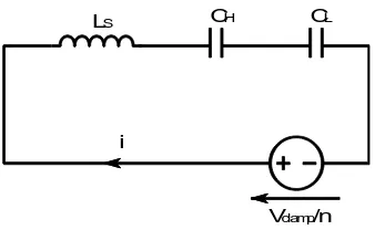
Initially, when the 2kA threshold level is triggered, the LV IGBT switch of the main branch is switched off. Hence, the current flows through the surge arrester AM as a bypass, creating a charging voltage for each capacitor in the auxiliary branch. Considering one auxiliary module, an equivalent charging circuit can be drawn as shown in Fig. 2c, where Vclamp/n is the effective charging voltage; LS represents the lumped stray module inductance; CH and CL are the HV and LV capacitors, respectively.
11
contain a number of IGBTs in parallel, CL must provide enough charge to gate all of these devices. Figure 2d shows the voltage waveform assumed on the LV capacitor CL during the IGBTs turn on process (the charge is assumed to be taken from the capacitor at a constant current during the turn-on time). After providing the required gate charge, the voltage across CL, VLV, drops to voltage VLV_E (which must be high enough to assure proper turn-on and correct operation of the associated electronic circuitry).
The CH and CL capacitors are designed by considering the resonant circuit formed by the capacitors and the stray inductance, LS, shown in Fig.2c. Since CL needs to be quickly charged to enable a fast response time of the auxiliary branch to the occurrence of a fault, the impedance of CH can be set much smaller than that of CL.
With the aim of achieving a compact system volume, the relationship between the two capacitors is further analysed to find the minimum value of the HV capacitor. Assuming the break down voltage of the LV arrester is relatively large, i.e. the LV capacitor voltage will not be clamped during the charging event, then the prospective voltage across the two capacitors is given by (6) and (7).
𝑉𝑃 = 𝑉𝐿𝑉+ 𝑉𝐻𝑉 = 2𝑉𝑐𝑙𝑎𝑚𝑝⁄𝑛 (6) 𝑉𝐻𝑉𝐶𝐻= 𝑉𝐿𝑉𝐶𝐿 (7)
Considering the gate charge requirement, Q, the voltage across the LV capacitor, VLV, drops to the end point voltage VLV_E (i.e. ≥ 15V) after the IGBT turn-on process.
𝑉𝐿𝑉_𝐸= 𝑉𝐿𝑉− 𝛥𝑉𝐿𝑉 = 𝑉𝐿𝑉−𝐶𝑄
𝐿 (8)
From (6) to (8), the relationship between the two capacitors can be derived as (9).
𝐶𝐻= 𝐶𝐿
2𝑉
𝐿𝑉_𝐸+ 𝑄𝐶𝐿
(𝑉𝑃− 𝑉𝐿𝑉_𝐸)𝐶𝐿− 𝑄
(9)
12
𝐶𝐿_𝑀𝐼𝑁 = 𝑉 𝑄
𝑃−𝑉𝐿𝑉_𝐸 (10)
Taking the derivative of CH with respect to CL (9), the corresponding value of CL that yields the minimum value for CH is given by
𝐶𝐿_𝐶𝑂𝑅 = 𝑉 𝑄
𝑃−𝑉𝐿𝑉_𝐸(1 + √ 𝑉𝑃
𝑉𝐿𝑉_𝐸) (11)
Substituting (11) into (9) yields,
𝐶𝐻_𝑀𝐼𝑁 = (𝑉 𝑄𝑉𝑃
𝑃 − 𝑉𝐿𝑉_𝐸)2. (1 + √ 𝑉𝐿𝑉_𝐸
𝑉𝑃 )
2 (12)
To reserve some charge for associated logic gate circuits and in this case assuming four parallel connected IGBTs, a charge of Q equal to 240µC is considered [26]. The corresponding CH and CL are obtained by solving (11) and (12), which yields approximately 15µF for both. Table 2 summarises the design results for each auxiliary module. The charging time of the LV capacitor can also be found,
𝑡𝐶𝐻𝐴𝑅𝐺𝐼𝑁𝐺 = 2𝜋√𝐿𝑆𝐶𝐿
[image:12.595.150.452.503.712.2]2 = 8.6µ𝑠. (13)
Table 2 Design results of auxiliary module
Symbol Description Value
LS Lumped stray
inductance
0.5µH
RS Discharge resistor 1Ω
CH High voltage capacitor 15µF
CL Low voltage capacitor 15µF
VLV Voltage after charging 31.25V
13 switching action
VHV_CLAMP Clamping voltage of
HV surge arrester
2.25kV
VLV_CLAMP Clamping voltage of
LV surge arrester
55V
4. Simulation results
[image:13.595.144.454.61.171.2]Figure 3a shows the schematic used to simulate the breaking of fault current by the proposed hybrid HVDC circuit breaker. An ideal switch (i.e. Fault Switch) emulates a short circuit fault or an open circuit condition according to the control order received.
[image:13.595.314.554.303.436.2]Fig.3a. Hybrid breaker performing current breaking action Fig3b. Current waveforms of the circuit breaker
Fig.3c. Zoomed Current waveforms of the circuit breaker Fig.3d. Voltage profiling of the circuit breaker
During normal operation, the LV IGBT and mechanical switch are closed, thereby supplying current to the load, R. A fault is created by closing the Fault Switch. When a fault threshold is reached, the LV
VDC
LV IGBT
Mechanical switch AM
L
R RCD + surge arrester Auxiliary HV arm
[image:13.595.45.281.477.604.2] [image:13.595.313.547.478.607.2]14
commutating IGBT is turned off. This causes the current to flow through the arrester, AM, as a bypass. The current pulse generated by AM is used to charge the two capacitors of each cell. The energy stored in CL is then used for turning on the HV IGBT in the auxiliary branch. Once the auxiliary branch is turned on, the current is fully commutated to it in a time determined by the value of the stray inductance. The mechanical switch is then turned off at zero current. When the mechanical switch is fully off, the HV IGBTs are turned off to commutate the current to the extinguishing branch, which reduces the current to zero.
Figures 3b and 3c show the current waveforms when the circuit breaker performs a fault current breaking action, where the curves represent the current through the main branch, the current through the auxiliary HV switch branch, the current through the extinguishing branch and the load side current. A fault occurs at a simulation time of 10ms, and the current starts to build up at the rate of 10kA/ms. Once the threshold of 2kA is met, the LV commutating IGBT is turned off. Therefore, the fault current flows through the surge arrester AM, and the two capacitors of each snubber circuit are charged by a current pulse. Once the auxiliary HV branch is turned on (after the LV capacitor is charged), the fault current is fully commutated to it in about 50μs, and the mechanical switch can then be opened at zero current with low voltage stress. After 500μs, the 80 auxiliary modules are turned off sequentially, in order to commutate the fault current into the extinguishing branch. As a result, the high voltage surge arrester string forces the fault current to reduce to zero. The total fault clearing time is about 2.75ms.
Figure 3d shows the corresponding voltage across the circuit breaker during this fault clearing event. The total 80 auxiliary modules have been further divided into 4 groups. When the mechanical switch contacts begin to open these 4 groups are sequentially switched off within 300μs. Therefore, a step-like voltage ramp is applied, which brings a significantly lower peak current seen by the HV IGBTs and less energy dissipated by the HV arresters.
15
snubber diode D. Figures 4b and 4c show the zoomed-in details indicating that the voltage across CL remains constant so we can use it for switching on the auxiliary arm cells.
Fig.4a. Voltage waveforms of one auxiliary module Fig.4b. Zoomed-in detail A
Fig.4c. Zoomed-in detail B
16
At a simulation time of 10.6ms, as shown in figure 4c, the HV IGBTs are turned off (staggered as discussed above). The fault current is then commutated to the associated RCD snubber plus surge arrester branch. CL is quickly charged and the voltage across it is clamped at 55V by AL, while the HV capacitor CH is charged to the breakdown level of AH. When the voltage produced by the circuit breaker equals the supply voltage 120kV, the fault current reaches its peak (i.e. at time 10.8ms).
The counter voltage produced by the surge arrester string is 1.5 times the supply voltage VDC (at the peak current) and forces the fault current to reduce to zero. When the fault current is cleared, the voltage across each module is 1.5kV (i.e. 1.5kVx80=VDC). Each CL is protected from discharge by the associated DS and DP.
[image:16.595.294.556.366.496.2]Figure 5a shows the total energy dissipation of the HV surge arrester during the current breaking action. Figure 5b compares the energy absorption of each auxiliary module in the different groups.
Fig. 5a. Total energy absorption by HV surge arrester string
Fig.5b. Energy absorption of each module in different groups
[image:16.595.55.307.366.498.2]17
5. Validation of the proposed hybrid HVDC circuit breaker
A scaled-down laboratory prototype of the proposed hybrid HVDC circuit breaker was used to validate the simulation results. The basic test set-up is as shown in Fig.6a. For simplicity and ease of implementation, a series connection of five HV cells was used for the auxiliary branch, with each HV auxiliary cell using a single IGBT.
Operation of the circuit is as follows. A capacitor bank is charged to the operating voltage (VDC) from a rectifier source. Following isolation of the source from the capacitor bank, a semiconductor switch is used to emulate a fault and current rises in the main branch (which is already gated on) limited by the inductor. When the threshold current is detected, the LV IGBT of the main branch is turned off. Hence, the fault current flows through the surge arrester, AM, as a bypass resulting in a charging voltage to charge the capacitors CL and CH of each cell. A summary of the parameters used for the experimental validation is given in Table 3.
The LV switching device is implemented using a 3.3kV/1.2kA IGBT from Dynex Semiconductor Ltd.. A similar device is used to emulate the operation of the ultra-fast mechanical switch. An auxiliary arm comprising five HV IGBTs rated at 1.7kV, 800A is used to demonstrate the capabilities of the hybrid HVDC circuit breaker. A PCB was used to interface the HV IGBTs with surge arresters and RCD snubber circuit as shown in Fig.6b.
18
[image:18.595.189.412.119.272.2]as the voltage requirement is achieved, the controller sends an acknowledgment signal to the circuit to gate the IGBT. A push-pull arrangement is used to achieve the required current gain to drive the IGBT.
Fig.6a. Test rig outline
[image:18.595.61.313.304.494.2]Fig.6b. Auxiliary branch module Fig.6c. Self-powered gate drive circuit
Table 3 Parameters used for validation
Symbol Description Value
VDC DC supply voltage 2.5kV
L DC inductor 2.5mH
CBANK Capacitor bank 2mF
VDC
Host PC Controller
Auxiliary and Extingishing Branch
Main Branch Cell 1 Cell 2 Fault Switch Cell 3 Cell 4 Cell 5 LV I GBT Mech Switch 5V
15V CLV
30R IGBT Local 5V
regulator
7n 500R
250R 80.6R
60k
5V
Signal to FPGA "charging"
[image:18.595.144.452.594.710.2]19
IBREAK Breaking current 600A
CL LV capacitor 15µF
CH
AAUX
HV capacitor
Auxiliary arm surge
arrestors in cells 1-5
15µF
EPCOS 340V, 595V,
1025V, 1025V, 1025V
6. Experimental results
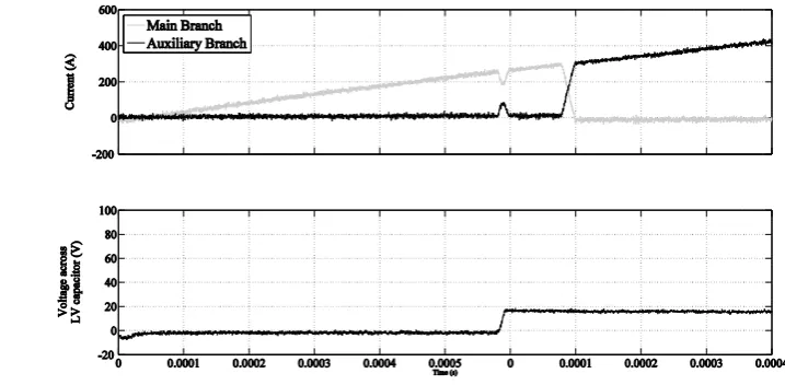
Experimental results are presented in this section to validate the operation of the proposed hybrid HVDC circuit breaker. A capacitor bank is charged to the operating voltage (2.5kV) from a source. Following the isolation of the source from the capacitor bank, the fault switch is engaged and current rises in the main branch (which is already gated on). When the threshold for fault current is detected (200A in this case), the LV IGBT of the main branch is turned off, while the auxiliary branch remains off. Hence, the fault current flows through the surge arrester AM as a bypass resulting in a charging voltage for the CL and CH capacitors in the auxiliary arm. The charging time is approximately 20µs - 30µs representing a half cycle of the resonant period created by the series combination of the two 15µF capacitors and the loop inductance (about 5µH). No additional inductance was used, since the inherent stray inductance in the construction was adequate. Clearly, in a circuit breaker built at full voltage the self-inductance created by the valve layout would likely be large enough that no inductance would need to be added- care must be taken to limit the inductance, however, since it affects the commutation time from the main branch onto the auxiliary branch.
20
[image:20.595.112.484.335.513.2]Figure 7a shows the current through the main branch, auxiliary branch and the voltage across the LV capacitor during the current build-up, resonant charging, current commutation and breaking periods. A detailed view of the current build-up, resonant charging and current commutation events is shown in Fig. 7b. It should be noted that the spikes and notches in the LV capacitor voltage waveform are a result of the high dv/dt and changes in common mode voltage which cannot be rejected by the differential probe used. The results in Figs. 7a and 7b are consistent with those shown in Fig. 3b and 3c, and therefore validate these simulation results.
21 Fig.7b. Zoomed-in detail of main branch current, auxiliary branch current and LV capacitor voltage
Fig.7c. Experimental reactor current and mechanical switch voltage
The fault current through the DC reactor and voltage seen by the mechanical switch during the fault clearing event are shown in Fig.7c. Five cells were used for the auxiliary branch. When the mechanical switch is ready, these five cells are switched off within 400µs, i.e. 100µs delay between each other. Thus, a step-like voltage ramp is applied as shown in the lower plot of Fig. 7c.
22
Fig.8. Complete experimental waveforms
7. Conclusion
23
8. References
[1] Kirby, N., Xu, L., Luckett, M., Siepmann, W.: “HVDC transmission for large offshore wind farms,” Power
Eng. J., vol. 16, pp. 135–141, Jun. 2002.
[2] Lu, W., Ooi, B.: “Optimal acquisition and aggregation of offshore wind power by multi-terminal voltage-source
HVDC,” IEEE Trans.Power Del., vol. 18, no. 1, pp. 201–206, Jan. 2003.
[3] Meyer, C., Hoeing, M., Peterson, A., DeDoncker, R. W.: “Control and design of DC grids for offshore wind
farms,” IEEE Trans. Ind. Appl., vol. 43, no. 6, pp. 1475–1482, Nov./Dec. 2007.
[4] DLR, German Aerospace Center, Institute of Technical Thermodynamics, Section Systems Analysis and
Technology Assessment, “Trans-Mediterranean interconnection for concentrating solar power,” Tech. Rep., 2006.
[Online]. Available: http://www.dlr.de/tt/trans-csp
[5] Franck, C.M.: “HVDC Circuit Breakers: A Review Identifying Future Research Needs, IEEE Trans. on Power
Delivery, vol. 26, pp. 998–1007, April 2011
[6] Billon, V., Taisne, J., Arcidiacono, V., Mazzoldi, F.: “The Corsican tapping: From design to commissioning tests
of the third terminal of the Sardinia-Corsica-Italy HVDC,” IEEE Trans. Power Del., vol. 4, no. 1, pp. 794–799, Jan.
1989.
[7] McCallum, D., Moreau, G., Primeau, J., Bahrman, M., Ekehov, B., Soulier, D.: “Multiterminal integration of the
Nicolet converter station into the Quebec-NewEngland Phase II HVDCtransmission system,” in Proc. CIGRE 35th
Int. Conf. on Large High Voltage Electric Systems, Paris, France, Aug./Sep. 1994, vol. 1, pp. 14-103/1–14-103/9.
[8] Greenwood, A., Kanngiessner, K., Lesclae, V., Margaard, T., Schultz, W.: “Circuit breakers for meshed
multiterminal HVDC systems Part I: Introduction DC side substation switching under normal and fault conditions,”
Electra, no. 163, pp. 98–122, Dec. 1995.
[9] Greenwood, A., Kanngiessner, K., Lesclae, V., Margaard, T., Schultz, W.: “Circuit breakers for meshed
multiterminal HVDC systems. Part II: Switching of transmission lines in meshed MTDC systems,” Electra, no. 164,
pp. 62–82, Feb. 1996.
[10] Bergstrom, L., Juhlin, L.E., Liss, G., Svensson, S.: “Simulator study of multiterminal HVDC system
24
[11] Kanngiesser, K., Ring, H., Wess, T.: “Simulator study on line fault clearing by DC circuit breakers in a meshed
MTDC system,” in Proc.Int. Conf. AC and DC Power Transmission, London, U.K., Sep. 1991, pp. 102–107.
[12] Häfner, J., Jacobson, B.: “Proactive Hybrid HVDC Breakers - A key innovation for reliable HVDC grids”, in
Cigré, Bologna, 2011, p. 0264.
[13] ABB, "EP0867998B1 Patent File," 1997.
[14] Grieshaber, W., Dupraz, J. P., Penache, D. L., Violleau, L.: “Development and test of a 120kV direct current
circuit breaker”, CIGRE 2014
[15] Wang, Y., Marquardt, R.: "Future HVgrids employing modular multilevel converters and hybrid
DC-breakers," Power Electronics and Applications (EPE), 2013 15th European Conference on , pp.1,8, 2-6 Sept. 2013
[16] Alstom, "Circuit Interruption Device” patent application EP2701254 (A1), 2012.
[17] Zhou, W., Wei, X., Zhang, S., Tang, G., He, Z., Zheng, J., Dan, Y., Gao, C.:, "Development and test of a
200kV full-bridge based hybrid HVDC breaker," in Power Electronics and Applications (EPE'15 ECCE-Europe),
17th European Conference, 2015
[18] Rieder, W.: “Circuit breakers Physical and engineering problems I—Fundamentals,” IEEE Spectr., vol. 7, no.
7, pp. 35–43, Jul. 1970.
[19] Rieder, W.: “Circuit breakers Physical and engineering problems II—Design considerations,” IEEE Spectr., vol.
7, no. 8, pp. 90–94, Aug. 1970.
[20] Rieder, W.: “Circuit breakers Physical and engineering problems III—Arc-medium considerations,” IEEE
Spectr., vol. 7, no. 9, pp.80–84, Sep. 1970.
[21] Flurscheim, C. H.: “Power Circuit Breaker Theory and Design”, Stevenage,U.K.: Peregrinus, 1985, pp. 556–
557.
[22] Brice, C. W., Dougal, R. A., Hudgins, J. L.: “Review of technologies for current-limiting low-voltage circuit
breakers,” IEEE Trans. Ind. Appl., vol. 32, no. 5, pp. 1005–1010, Sep./Oct. 1996.
[23] Hoerauf, R. G., Shipp, D. D.: “Characteristics and applications of various arc interrupting methods,” in Proc.
25
[24] Atmadji, A. M. S., Sloot, J. G. J.: “Hybrid switching: A review of current literature,” in Proc. Rec. IEEE EMPD
Conf., Mar. 3–5, 1998, vol. 2, pp. 683–688.
[25] Twenties Project Deliverable 11.3 “Testing results from DC network mock up and DC breaker demonstrator
Status Report for European commission” Available: http://www.twenties-project.eu/system/files/D11.3-Final.pdf,
2013
[26] Dynex Semiconductor Ltd. (2012): DIM1200ESM33-F000 Single Switch IGBT Module. Available:
![Table 1 Specification for proposed hybrid HVDC circuit breaker [25]](https://thumb-us.123doks.com/thumbv2/123dok_us/8600102.372385/5.595.144.451.336.542/table-specification-proposed-hybrid-hvdc-circuit-breaker.webp)