1
Characterisation and Modelling of Gallium Nitride
Power Semiconductor Devices Dynamic On-state
Resistance
Ke L
I,
IEEE Member
, Paul E
VANS, Mark J
OHNSON,
IEEE Member
Abstract—GaN-HEMTs suffer from trapping effects which in-creases device ON-state resistance (RDS(on)) above its theoretical
value. This increase is a function of the applied DC bias when the device is in its OFF state, and the time which the device is biased for. Thus, dynamic RDS(on) of different commercial
GaN-HEMTs are characterised at different bias voltages in the paper by a proposed new measurement circuit. The time-constants associated with trapping and detrapping effects in the device are extracted using the proposed circuit and it is shown that variations in RDS(on)can be predicted using a series of
RC circuit networks. A new methodology for integrating these
RDS(on)predictions into existing GaN-HEMT models in standard
SPICE simulators to improve model accuracy is then presented. Finally, device dynamicRDS(on)values of the model is compared
and validated with the measurement when it switches in a power converter with different duty cycles and switching voltages.
Index Terms—GaN-HEMT; Dynamic ON-state resistance;
Power semiconductor device characterisation; Power semicon-ductor device modelling; Equivalent circuit
I. INTRODUCTION
B
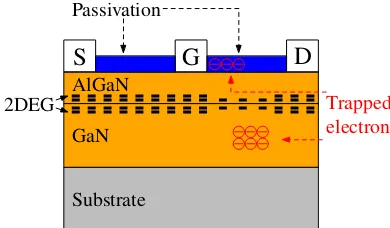
ECAUSE of small device ON-state resistance and inter-electrode capacitance, gallium nitride (GaN) power semi-conductor devices produce low power loss in electrical energy conversion. Thus, it is interesting to apply GaN devices in high frequency, high efficiency and high power density power converters [1]–[3]. Understanding GaN devices characteristics is very helpful to better use those devices in power electronics systems. High-Electron-Mobility Transistors (HEMTs) are the most widely used GaN power electronic devices, but they suffer from electron trapping effects that decreases device performance [4], [5].It is reported by authors in [6], [7] that GaN-HEMT trapping effects can be attributed to device surface trapping and buffer layer trapping. As shown in [6], when GaN-HEMT is biased, the electrical field between drain and gate terminal causes some electrons to be trapped at the surface close to the gate. Meanwhile, large vertical electrical field under the drain terminal causes some electrons to be trapped in device buffer layer. All the trapped electrons are not freed instantaneously when device changes from OFF-state to ON-state, which reduces device ON-state current carrying capability by two-dimensional electron gas (2DEG). Trapped electrons positions and their influence on 2DEG is illustrated in Fig. 1. Some techniques, such as employing appropriate passivation and filed plate structures, using p-GaN layer to device Drain electrode [8] and optimizing device buffer layer design [9] in device fabrication, can help to alleviate trapping effect.
S
G
D
Passivation
AlGaN
GaN
Substrate
[image:1.612.335.530.198.312.2]Trapped electron 2DEG
Fig. 1: Trapped electrons positions and their influence on 2DEG in a GaN-HEMT
t VDS
t1 t2 t3
0
RDS(on)
Trapping time Detrapping time 1st bias voltage
2nd bias voltage 1st dynamic
RDS(on)
2nd dynamicRDS(on)
StaticRDS(on)
Fig. 2: GaN-HEMT dynamicRDS(on) values due to trapping
effects
The reduced GaN device current conduction capability caused by the trapping effect increases device channel resis-tance, which is important for power converters design when considering efficiency and cooling system size. Illustrated in Fig. 2, this trapping effect is related mainly with two parameters when device in OFF-state, one is the bias VDS voltage value and another is the bias time (trapping time), which would give rise to the increase of GaN device ON-state resistance (RDS(on)) value. In the ON-state, detrapping process occurs and theRDS(on) values decrease to the static value at a rate characterized by detrapping time. In [10], authors present that GaN deviceRDS(on) values would increase by a maximal factor of 4 after 1ms bias time depending on biasVDSvoltage value, while device dynamic RDS(on) values would decrease 30% after 10µs detrapping time. Authors in [11] show that
device dynamic RDS(on) values would reach more than 10
[image:1.612.316.562.359.482.2]When employing GaN transistors in power electronics cir-cuits, GaN devices normally switch with different periods and duty cycles leading to a combination of trapping and detrapping effects and consequently uncertainty in the actual value ofRDS(on). This will lead to uncertainty in device power loss, making predictions of converter efficiency and cooling system design challenging. As only device static RDS(on) values are given in its technical datasheet, the ability to
characterise and model GaN-HEMT dynamicRDS(on) values
is thus an important design consideration.
Two different methods are commonly used to measure
GaN-HEMT dynamic RDS(on) values: one method is by using
directly a measurement equipment [12], and another one is by using an electrical circuit, where different circuit topologies are proposed by authors in [10], [11], [13]–[15]. In this paper, a new characterisation circuit is presented to measure
GaN-HEMT dynamic RDS(on) values, which can be easily
imple-mented. Compared to the above different circuits, this new measurement circuit needs fewer components and offers an alternative method to characterise the device and to compare the results.
Regarding device dynamic RDS(on)values modelling, it is not addressed in the reported GaN-HEMT models using for power electronics simulation [16], [17] and it is not included in the models offered by device manufacturers. For this reason,
based on device dynamic RDS(on) measurement results, an
equivalent circuit is thus proposed in the paper to present device trapping and detrapping effect, which can be used in a circuit simulator to study device RDS(on)variation when it switches in a power converter.
Initial GaN-HEMT dynamic RDS(on)characterisation and modelling results are reported by authors in [18]. More device
dynamic RDS(on)measurement results together with more
analysis on simulation and experimental results are presented in this work.
The paper is structured with following sections. First the measurement circuit to characterise GaN-HEMT dynamic
RDS(on) values is presented. Afterwards, measurement results of different trapping and detrapping time on RDS(on) values are shown. Based on the measurement results, a model using equivalent circuit is proposed to represent device dynamic
RDS(on) values. The model is further validated by comparing with the measurement when device switches in a power converter. Finally some conclusions are given.
II. GAN-HEMTDYNAMICON-STATE RESISTANCE
MEASUREMENT
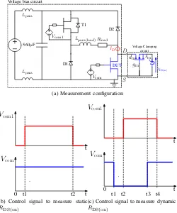
A. Measurement circuit
GaN device RDS(on) values can be obtained by measuring device ON-state voltage VDS(on) across it and current ID through it in an electrical circuit. As the measured bias voltage when device is OFF (VDS(off)) can be more than several hundred times higher than deviceVDS(on), a voltage clamping circuit is necessary to reduce the measured VDS(off) in order to increase measurement accuracy, where a low voltage range probe can then be used, which is more accurate to measure small voltage than a high voltage range probe using in a direct
T1
D1 DUT
Vcom
Vcom1 R
load
560µF
Lpara Lpara
D2
D
S
ID Voltage Clampingcircuit
VDS(m.)
Lpara(load)
Voltage bias circuit
dm
gm
sm
(a) Measurement configuration
t
t Vcom1
Vcom
t1 t2
0
(b) Control signal to measure static RDS(on)
t
t Vcom1
Vcom
t1 t2 t3 t4 0
[image:2.612.314.564.56.356.2](c) Control signal to measure dynamic RDS(on)
Fig. 3: GaN-HEMT dynamic ON-state resistance measurement circuit and control signals
VDSvoltage measurement. For this reason, the measurement circuit shown in Fig. 3 is constituted by two parts: one is a voltage bias circuit to control device trapping time when it is OFF and another is a voltage clamping circuit to measure deviceVDS(on) value when it is ON.
In the voltage bias circuit, a transistor T1 is used to control DUT trapping time. A resistive load Rload is used to set the current level when DUT is in ON-state. Because of the parasitic inductanceLpara(load) of the Rload, two diodes D1, D2 offer a free wheeling path of the current when either T1 or DUT is switched from ON to OFF.
The voltage clamping circuit is constituted by a deple-tion mode (D-mode) Si-MOSFET and a Zener diode. DUT measurement voltage VDS(m.) is measured across the Zener diode as shown in Fig. 3a. The principle of the voltage clamping circuit is that when DUT is ON, D-mode
Si-MOSFET is in ON-state (Vgmsm is superior to MOSFET
threshold voltage Vth), so terminals sm and dm are almost in the same potential (Zener diode only reversely conducts a few microamperes, so its conduction loss do not affect
the measurement) and DUT VDS(on) can thus be measured
DUT D2
D1 T1
[image:3.612.312.563.53.204.2]Voltage clamping circuit Load
Fig. 4: Realization of the measurement circuit
between D-mode MOSFET and Zener diode, so VDS(m.) is
inferior to Zener diode clamping voltageVclampin steady state. Instead of measuring voltage range betweenVDS(on)andVDS, a much smaller voltage range between VDS(on) and Vclamp is measured, thus the measurement sensitivity is increased. Compared to the similar type voltage clamping circuits that are analyzed by authors in [14], fewer components and no external power supply are used in this clamping circuit.
Device static RDS(on) value can be measured by applying the control signal shown in Fig. 3b, where DUT is kept always in ON-state and T1 is controlled by a single pulse.
Device dynamicRDS(on) values can be measured by apply-ing the control signal shown in Fig. 3c, where DUT is initially kept in ON-state and T1 blocks all the bias voltage. Then at t1, DUT is switched OFF and at t2, T1 is switched ON, thus all the bias voltage is across DUT. Afterwards, at t3, DUT is switched ON again, so current ID flows through the DUT. Finally at t4, T1 is switched OFF. Thus, DUT trapping time is controlled by t2-t3 while detrapping time is controlled by t3-t4, soRDS(on) values under different trapping and detrapping time can be measured.
[image:3.612.74.276.54.186.2]The realization of the measurement circuit is shown in Fig. 4. In the measurement,Rload= 100Ω, T1 is a commercial GaN-HEMT (EPC2012C, 200V/5A) while D1 and D2 are the same Schottky diode (MBRS4201T3G, 200V/4A). Dynamic
RDS(on)values of a DUT, which is the same as T1, is measured by the above circuit, of which the results are presented in the next section.
B. Measurement results
Several major parameters of the measurement equipments and clamping circuit devices are summarized in TABLE. I.
In the measurement, the maximal measured VDS voltage is
3.3V, which can achieve a measurement accuracy of at least 3.3
28 = 0.013V by using an 8-bit resolution oscilloscope. In order to validate the proposed measurement circuit and demonstrate the dynamicRDS(on)effect in GaN-HEMTs,
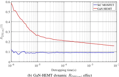
RDS(on)of a SiC-MOSFET (C3M0065090D, 900V/36A) with similar static RDS(on)value as GaN-HEMT is measured and set as a measurement benchmark, because SiC-MOSFET does not exhibit dynamicRDS(on)behaviour. Both devices are biased at 120V for 1ms. SiC-MOSFET is switched from 0V to 10V while GaN-HEMT is switched from -3V to 5V. The obtained measurement waveforms are compared in Fig. 5.
Time(µs)
0
VDS(m
.
)
(V)
-0.5 0 0.5 1
1.5 SiC MOSFET
GaN HEMT
ID
(V)
-0.5 0 0.5 1 1.5
2 4 6 8 10 12
Time(µs)
0 2 4 6 8 10 12
(a) Measured waveforms comparison when device biased at 120V for 1ms
Detrapping time(s)
10-6 10-5 10-4 10-3 10-2
RDS(on)
(Ω)
0 0.1 0.2 0.3 0.4 0.5 0.6
SiC MOSFET GaN HEMT
(b) GaN-HEMT dynamicRDS(on)effect
Fig. 5: Setting SiC-MOSFET as measurement benchmark to
demonstrate GaN-HEMT dynamic RDS(on)effect
Device conduction current ID and measurement voltage
VDS(m.)waveforms shown in Fig. 5a corresponds to the time range t3-t4 when applying gate signal of Fig. 3c. It is observed that because of the voltage clamping circuit,VDS(m.)is about 1.5V when DUT is OFF, which is much smaller than the bias voltage (120V), thus the measurement accuracy is improved in comparison to a direct measurement. It is also shown in the measurement results that measuredVDS(m.)is almost constant for SiC-MOSFET. However, it decreases for GaN-HEMT, indicating an obtained dynamicRDS(on)value variation.
When each electrical parameter stabilizes after OFF-ON transition, which is 1µs in the measurement, the device’s
dynamicRDS(on) values are calculated and they are compared in Fig. 5b.
As shown in the results, an almost constant RDS(on)value is obtained for SiC-MOSFET1, indicating no trapping effect
for this device. The obtainedRDS(on)value is close to device datasheet value, which helps to validate the proposed measure-ment circuit. In contrary to that, the obtained RDS(on)value of GaN-HEMT is higher than its static RDS(on)value, which shows that device suffer from a trapping effect after 120V
and 1ms bias. Device RDS(on)value then decreases with
1ObtainedR
[image:3.612.312.562.226.388.2]TABLE I: Major parameters of the measurement equipments and clamping circuit devices
Oscilloscope Current probe Voltage probe D-mode MOSFET Zener diode
64xi (600MHz, 8-bit) CP030 (50MHz, 30A) ZD1500 (1.5GHz, 8V) BSP149 (200V,Vth≈ −1.4V) BZT52C3V3 (3.3V)
RDS(on)
(Ω)
10−6
100 10−2
10−4 101
DynamicRDS(on)(120V) StaticRDS(on)
DynamicRDS(on)(80V)
[image:4.612.307.561.67.435.2]10−1 10−3 10−5
Fig. 6: Comparison of GaN-HEMT (EPC2012C) static and dynamic RDS(on) values at 20◦C
detrapping time, showing a detrapping effect influence.
At 20 ◦C, dynamic R
DS(on)of the GaN-HEMT is thus characterized with applied bias voltages of 80V and 120V under different trapping time and detrapping time, where the measurement results are shown in Fig. 6.
As shown in the results, device dynamic RDS(on) values increase with trapping time and it decreases with detrapping time, and it increases more under a higher bias voltage. For this device, it is observed that when device biased by a certain trapping time, it needs a longer detrapping time to reduce its dynamicRDS(on)values to the static values, which shows that effectiveRDS(on)values are likely to be higher than theoretical values due to this trapping effect, especially in higher voltage applications with low duty cycles.
It is also observed in Fig. 6 that the device suffers from fast trapping effect that only 1µs trapping time can increase itsRDS(on)value. Between 1µs to 100µs, slow trapping effect occurs, so device RDS(on)values vary a little by trapping time. After 100µs,RDS(on)values increase again with trapping time until 1s. In terms of detrapping effect, it is observed in Fig. 6 that device has fast detrapping effect from 1µs to 10µs,
where deviceRDS(on)values decrease about a half. Then from 10µs to 1s, RDS(on)decreases slowly with detrapping time. After 1s, another fast detrapping effect is observed. Those characterization results correspond to the GaN device trapping and detrapping time constants presented by authors in [19].
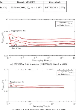
It is to be noted that by choosing devices T1, D1, D2 and D-mode MOSFET to corresponding DUT power ratings, the presented measurement circuit can be used to characterise dynamicRDS(on)of different commercial GaN transistors with different voltage and current ratings, where the measurement results are shown in Fig. 7 for a 650V/15A GaN transistor (GS66504B) from GaNSystems and another 100V/1A GaN transistor from EPC (EPC2036).
For transistor GS66504B, as shown in Fig. 7a, when biased
10-6 10-5 10-4 10-3 10-2 10-1 0.05
0.1 0.15 0.2
StaticRDS(on) DynamicRDS(on)
Trapping time: 10s
10ms 1s
100ms RDS(on)
(Ω)
Detrapping Time(s)
(a) 650V/15A GaN transistor (GS66504B) biased at 400V
100-6 10-5 10-4 10-3
0.05 0.1 0.15
RDS(on)
(Ω)
Detrapping Time(s)
StaticRDS(on) DynamicRDS(on)
Trapping time: 10s 1s
(b) 100V/1A GaN transistor (EPC2036) biased at 100V
Fig. 7: Dynamic RDS(on) measurement results of different GaN transistors
at 400V for 10s, device maximal RDS(on) value increase to around 65% in comparison with its staticRDS(on) value. For transistor EPC2036, as shown in Fig. 7b, when biased at 100V for 10s, device maximalRDS(on)value increase to around 30% in comparison with its staticRDS(on) value, which shows less dynamic RDS(on)variation.
In order to study GaN-HEMT RDS(on)values variation
when device applied in power converter, a device trapping and detrapping model is proposed based on the measurement results, which will be presented in the next section.
III. GAN-HEMTDYNAMICON-STATE RESISTANCE
MODELLING
A. Trapping and detrapping model
Device static RDS(on)values can be modulated by the
applied VGS gate voltage. Characteristics for the EPC2012C device are shown in Fig. 8, but this applies to all GaN transistors.
According to thisRDS(on)-VGSrelation, the obtained device
dynamic RDS(on) values can be represented by its static
[image:4.612.53.303.68.282.2]VGS(V)
2 2.5 3 3.5 4 4.5 5
RDS(on)
(Ω)
0 0.5 1 1.5 2
A
[image:5.612.50.298.55.186.2]B Vcomp
Fig. 8: Device staticRDS(on) values of differentVGS voltages at 20◦C
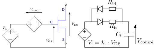
where point A corresponds to the device staticRDS(on)value, and point B corresponds to the device RDS(on) value after certain trapping time. The VGS voltage difference between point A and point B, which is defined as Vcomp, is applied to representRDS(on) variation during trapping and detrapping process. After adding Vcomp in gate circuit, which is shown in Fig. 9a, device effective VGSvoltage (VGS=VG−Vcomp) after trapping and detrapping time is adjusted, thus a dynamic
RDS(on) value is obtained. According to the reported trapping mechanism of GaN device by different researchers in [6], [9], [20], no matter the origin of the trapping is from either device gate electrode or device buffer layer, the consequence is that those trapped electrons would deplete 2DEG channel, resulting a decreased current conduction capability and device dynamic RDS(on)degradation. Using Vcompin the proposed model is able to model device current conduction capability, even though it is an equivalent circuit, it still represents device physical behaviour.
In order to modulate device effective gate voltage, Vcomp value increases with the trapping time and it decreases with the detrapping time. Vcompcan then be further modelled in the form of an RC circuit, which is presented in Fig. 9b. In one RC unit, Vcompi increases when capacitor Ci is charged by a controlled voltage source Vi through resistor Rit and it decreases when Ci is discharged through resistor Rid. As defined by the following equation eq.(1), Vi values are expressed by multiplying a coefficient ki to the device bias voltageVDSwhen device is OFF and Vi values are zero when device is ON.
Vi=ki·VDS (Device is OFF)
Vi= 0 (Device is ON)
(1)
After trapping timet1and detrapping timet2,Vcompivalues can be easily obtained by the following equations.
Vcompi(t1) =Vi·
1−exp
−R t1
it·Ci
(2)
Vcompi(t2) =Vcompi(t1)·
exp
−R t2
id·Ci
(3)
In order to model different trapping and detrapping time
Vcomp D
S G
VG
VDS
VGS
(a) UsingVcomp to represent device effective gate voltage
Vi=ki·VDS Vcompi
Ci
Rit
Rid
(b) Using RC unit to representVcomp
Fig. 9: DynamicRDS(on) values representation by equivalent circuit
constants observed in the characterisation results, a series of the RC units are used in the model, soVcompvalue is the sum of the capacitor voltage in each unit.
Vcomp= n X
i=1
Vcompi (4)
By obtainingVcompvalue, device effectiveVGSvoltages can be obtained at different trapping and detrapping time, so device dynamic RDS(on)values can be finally obtained based on the
RDS(on)-VGSrelation shown in Fig. 8.
RDS(on) =f(VGS) =f(VG−Vcomp) (5)
It is shown in the measurement results that device dynamic
RDS(on)values increase in a higher bias voltage, indicating a biggerVcompvalue in the model after same trapping time. In order to apply the proposed model in different bias voltages and easily implement it in the simulation software, only ki is chosen as a function of bias voltage (ki = f(VDS)), because its trend is easier to be found (variation within one order of magnitude) and to be implemented in the model than other parameters (variation may exceed more than one order of magnitude). Thus, in the model, following number of parameters need to be determined: Pn
i=1{
Ci, Rid, Rit, ki1, ki2}, where n is the number of RC units used, ki1 and ki2 are different coefficients at different bias voltagesVDS1andVDS2. All the above parameters in the model are needed to be extracted and the results are presented in the next subsection.
B. Model parameters extraction
Illustrated in Fig. 10, a fitting method is used to minimize the error of the following equation:
error=RDS(on)(fitted,VDS=80V)−RDS(on)(measured,VDS=80V)
2
+RDS(on)(fitted,VDS=120V)−RDS(on)(measured,VDS=120V)
2 (6) where fitted RDS(on)values can be obtained from eq.(2)-eq.(5).
The fitting function starts with initial parameters X0 and attempts to find adequate parameters X in order to minimize
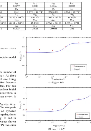
[image:5.612.308.564.66.149.2]TABLE II: Parameters using to represent GaN-HEMT trapping and detrapping effect in the model
k11 k21 k31 k41 k51 k61 k71
0.0015 0.0013 0.0039 0.0297 0.0013 0.0046 0.0256
C1 C2 C3 C4 C5 C6 C7
8.8F 3.92×10⁻⁹F 0.314F 351F 6.678×10⁻⁵F 952.038F 3.051×10⁻⁸F
R1t R2t R3t R4t R5t R6t R7t
0.043Ω 0.0019Ω 0.0025Ω 5.416×10⁶Ω 0.011Ω 2.567×10³Ω 0.206Ω
R1d R2d R3d R4d R5d R6d R7d
1.673×10⁶Ω 2.185×10³Ω 1.609×10⁵Ω 8.261×10⁴Ω 47.188Ω 6.756×10⁷Ω 1.305×10⁸Ω
k12 k22 k32 k42 k52 k62 k72
0.0011 0.0019 0.0012 0.0027 0.0015 0.00088 0.02
Initial parameters
X0=
n
P
i=1{
Ci0, Rid0, Rit0, ki10, ki20} Fitting function
RDS(on)(fitted)
RDS(on)(measured)
X, error Xj,errorj∈min{error1, ..., errorm}
[image:6.612.246.555.63.508.2]j
Fig. 10: Flowchart when using fitting method to obtain model parameters
values, because it is found that the increase of the number of RC units does not help decrease the error further. As there are 35 parameters to be determined in the model, one fitting process might result in a local error minimization, because fitting result is dependent on its initial parameters. For this reason, enough fitting iterations are tried with random initial parameters to guarantee that a global error minimization is achieved. Model parameters Xj are obtained whenerrorj is the minimal value of all the iterations.
All the obtained parametersk11-k71,C1-C7,R1t-R7t,R1d
-R7d and k12-k72 are given in TABLE. II. The compari-son between the model and the measurement on dynamic
RDS(on)values as a function of trapping and detrapping times at different bias VDSvoltages are shown in Fig. 11 and in Fig. 12 separately. It is to be noted thatRDS(on)values shown in Fig. 11 are the values obtained 1µs after OFF-ON transition
which explained in section II-B.
As shown in Fig. 11, device RDS(on)values show almost no change when the trapping time is varied between 1µs and 100µs, which leads to almost overlapping detrapping curves
at 1µs, 10µs and 100µs trapping time shown in Fig. 12.
In Fig. 12a, when device is biased at 80V, maximal error
between model and measurement is about 0.018Ω, which
corresponds to a maximal 13% difference. The model yields an average 4% difference to the measurement. It is found that in the results shown in Fig. 12b when device is biased at 120V, the maximal error between model and measurement is about 0.097Ω, which corresponds to a maximal 23% difference. The average difference between model and measurement in this condition is about 6%. Despite those difference, it is shown
that the model generally follow measured RDS(on)values
variation over 6 orders of magnitude of time, so it can be stated that the model represents the measurement in a reasonable way.
Once all the above parameters are obtained, for any bias voltage VDSx betweenVDS1 andVDS2, its corresponding Vix value used in the model can be obtained by a numerical
100-6 10-5 10-4 10-3 10-2 10-1 0.05
0.1 0.15 0.2
Trapping time(s)
RDS(on)
(Ω)
Measurement Model
(a)VDS= 80V
100 -6 10-5 10-4 10-3 10-2 10-1
0.2 0.4 0.6 0.8 1 1.2
Trapping time(s)
RDS(on)
(Ω)
Measurement Model
(b)VDS= 120V
Fig. 11: Comparison between the measurement and model on dynamic RDS(on) values as a function of trapping time at different bias VDS voltages
interpolation of Vi1 and Vi2. Here, a linear interpolation method is chosen to reduce model computational complexity, soVix value can be obtained by eq.(7).
Vix= Vi2−Vi1
VDS2−VDS1×
(VDSx−VDS1) +Vi1 (7)
Finally, coefficientskix used in the model can be obtained by eq.(8).
kix=
VDS2·ki2−VDS1·ki1
VDS2−VDS1 ×
(VDSx−VDS1)
VDSx
+VDS1 VDSx ·
100-6 10-5 10-4 10-3 10-2 10-1 0.05
0.1 0.15 0.2 0.25
Detrapping time(s)
RDS(on)
(Ω)
Measurement Model
1µs
10µs 100µs 1ms
10ms
Trapping time: 100ms
(a)VDS= 80V
100-6 10-5 10-4 10-3 10-2 10-1 0.2
0.4 0.6 0.8 1 1.2
Detrapping time(s)
RDS(on)
(Ω)
Measurement Model
1µs
10µs 100µs 10ms
Trapping time: 100ms
1ms
(b)VDS= 120V
Fig. 12: Comparison between the measurement and model on dynamic RDS(on) values as a function of detrapping time for different trapping times and at different bias VDSvoltages
be represented by voltage controlled voltage source. It is also to be noted that the proposed model can be easily added in the behavioural model proposed by manufacturers to study device trapping effect, which is normally missing in those manufacturer behavioural models.
As GaN-HEMT suffered from trapping effect, its RDS(on) values might increase when it switches continuously in a power converter. For this reason, RDS(on) values estimated by the above model are compared with the measurement, and the results will be presented in the next section.
IV. MODELVALIDATION
A. Model validation at different switching voltages
The same electrical circuit shown in Fig. 3a with the control signal shown in Fig. 13 is used to measure device dynamic RDS(on) values when it switches continuously. In order to avoid the influence of switching losses of both DUT and D-mode MOSFET of the voltage clamping circuit on device temperature, it switches at 10kHz with a duration of 0.1s. In the measurement, sampling time is 400ns. Device
RDS(on)mean value between 1µs and 3µs after OFF-ON transition is chosen as its trapping value of each switching cycle, while its detrapping value is calculated at the end of each ON-state.
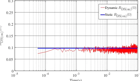
The same SiC-MOSFET is tested at first in order to compare its static and dynamic RDS(on)values when device switches
t t
V
com1V
comt1 t2
0
t1 t2
[image:7.612.48.311.53.363.2]0
Fig. 13: Control signal when device switches continuously in a power converter
Time(s)
100-5 10-4 10-3 10-2 10-1
0.05 0.1 0.15 0.2 0.25 0.3
RDS(on)
(Ω)
DynamicRDS(on)(Ω)
StaticRDS(on)(Ω)
Fig. 14: SiC-MOSFET measured static and dynamic
RDS(on)values comparison
continuously (10kHz, 50% duty cycle), of which the result is shown in Fig. 14.
As shown in the measurement results, obtained
SiC-MOSFET dynamic RDS(on)values when device switches
re-mains the same as its staticRDS(on)value obtained previously, indicating a constant deviceRDS(on)value.
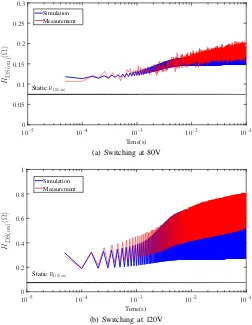
Afterwards, the same GaN-HEMT device is switched under different conditions. When switching voltages are 80V and 120V with 50% duty cycle (corresponding to 50µs trapping
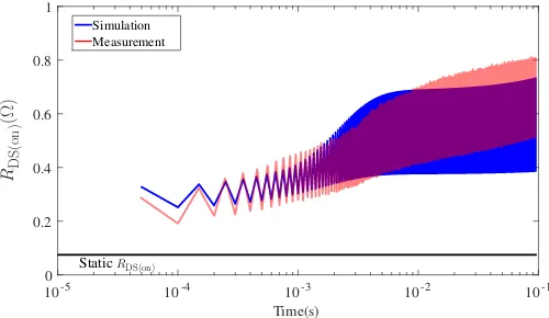
and detrapping time), the comparison between the measure-ment and simulation of device RDS(on) values is shown in Fig. 15a and in Fig. 15b separately.
In Fig. 15a, measured deviceRDS(on)values increase to a factor of around two higher than its static value after 0.1s, be-cause device trapping time constants are faster than its detrap-ping time constants as shown in Fig. 6. Furthermore, trapdetrap-ping effects can increase deviceRDS(on) values very quickly when trapping time inferior to 10µs, which indicates that device effective RDS(on)values are likely to be bigger than its static value if switching frequency increases to more than 100kHz. When comparing the simulation with the measurement, the simulation results represent well the measurement, which con-firms theRDS(on)increase trend. Meanwhile, there are mainly two mismatches between the model and the measurement: one is that model estimates smaller RDS(on)trapping values of each switching cycle, because model produces smaller
RDS(on)values than the measurement after different trapping time (see Fig. 11a); another is that model estimates smaller
RDS(on)values ripple after each cycle, because model pro-duces smallerRDS(on)values variation after 50µs detrapping time (see Fig. 12a).
[image:7.612.315.561.165.307.2]Time(s)
100 -5 10-4 10-3 10-2 10-1
0.05 0.1 0.15 0.2 0.25 0.3
RDS(on)
(Ω)
Simulation Measurement
StaticRDS(on)
(a) Switching at 80V
Time(s)
100-5 10-4 10-3 10-2 10-1
0.2 0.4 0.6 0.8 1
RDS(on)
(Ω)
Simulation Measurement
StaticRDS(on)
[image:8.612.317.563.54.206.2](b) Switching at 120V
Fig. 15: Comparison between the measurement and simulation on RDS(on) values when device switches at 80V and 120V (50% duty cycle)
device produces a biggerRDS(on)value which reaches almost 10 times bigger than its static RDS(on)value at the end of 0.1s due to trapping effect. RDS(on)ripple is bigger than that observed in the measurement results when device is biased at 80V, which reveals a bigger influence of detrapping effect on device RDS(on)value. Similar to the measurement results in Fig. 15a, device RDS(on)values keeps increasing because of the same reason.
When comparing the simulation with the measurement, the increase trend of device RDS(on)values andRDS(on)trapping values of each switching cycle are represented well by the model. However, the main mismatch is on device
RDS(on)detrapping values of each cycle, where notably that the model estimates a biggerRDS(on)ripple than the measure-ment after 500µs.
Despite the difference between the model and the mea-surement on device RDS(on)detrapping values illustrated in Fig. 12b which may cause the above mismatch, it is found that characterised deviceRDS(on)variation due to detrapping effect does not correspond to the values observed in each switching cycle. In Fig. 12b, for 1ms and 10ms measurement curves,
RDS(on)variation after 50µs detrapping time is about 0.4Ω and 0.5Ω. In contrary, at the same time range when device
switches, the RDS(on)variation is only about 0.2Ωand 0.25Ω as shown in Fig. 15b.
100 -6 10-5 10-4 10-3 10-2
0.2 0.4 0.6 0.8 1 1.2
Detrapping time(s)
RDS(on)
(Ω)
Tj = 60◦C Tj = 20◦C
100µs 10ms Trapping time: 100ms
1ms
Fig. 16: DeviceRDS(on)comparison of differentTj
It is supposed that with the increase of the device effective
RDS(on)value, the conduction losses might increase the device junction temperatureTjdue to the poor thermal impedance of the packaging (device mounted onto an FR4 PCB substrate, which yields a big device junction to ambient thermal resis-tance up to 85◦C/W found in device datasheet). The
temper-ature difference might cause variation on charcterised device
RDS(on)values. In order to validate this hypothesis, device is characterised again at 60◦C with the same characterisation
method.
B. Temperature influence on deviceRDS(on)values
Device RDS(on)values at different temperatures are com-pared in Fig. 16. As shown in the results, device junction temperature Tj mainly influence on device detrapping effect, where it is illustrated that device RDS(on)values are bigger in 60◦C than in 20◦C in the detrapping time range from
10µs to 100µs, which results a smaller RDS(on)ripple. This characterisation result seems to be consistent with the obtained
RDS(on)values when device switches in Fig. 15b.
In order to further investigate the influence of the new characterisedRDS(on)values on device switching, the param-eters in the model is adjusted by using the characterised
RDS(on)values at 60◦C when device biased at 120V. The curve fitting process is the same as described in section III-B. The new parameters using in the model (see TABLE IV) and the comparison between the model and the measurement on deviceRDS(on)values (see Fig. 20 and Fig. 21) are given in APPENDIX.
After obtaining the new parameters, the comparison between the model and the measurement on device
RDS(on)values when it switches at 120V is shown in Fig. 17. The model estimates device RDS(on)values more closer to the measurement than previous results in Fig. 15b. Thus, the hypothesis that the measurement and model difference due to
Tjdifference can be validated.
[image:8.612.48.300.55.380.2]Time(s)
100-5 10-4 10-3 10-2 10-1
0.2 0.4 0.6 0.8 1
RDS(on)
(Ω)
Simulation Measurement
[image:9.612.49.299.55.200.2]StaticRDS(on)
Fig. 17: Comparison between the measurement and simula-tion (with new parameters) on RDS(on) values when device switches at 120V
Time(s)
100 -5 10-4 10-3 10-2 10-1
0.05 0.1 0.15 0.2 0.25 0.3
RDS(on)
(Ω)
Simulation Measurement
StaticRDS(on)
(a) Device switches at 80V (90% duty cycle)
100-5 10-4 10-3 10-2 10-1
0.1 0.2 0.3 0.4 0.5 0.6
Time(s) RDS(on)
(Ω)
Simulation (Presented model)
Measurement
StaticRDS(on) Simulation (EPC PSpice model+Presented model)
(b) Device switches at 100V (50% duty cycle)
Fig. 18: Comparison between the measurement and simulation onRDS(on) values when device switches at different voltages and duty cycles
average conduction power loss increase to 1.8 times bigger
than the duty cycle is 50%, which might cause device Tj
increase, resulting in RDS(on)values mismatch observed in Fig. 18a. The mismatch observed in Fig. 18b is supposed to be the linear interpolation method used in the model. More complexly numerical interpolation methods can be used in the model, however it might make model unsuitable for a circuit simulator. Despite some difference between the model and the measurement, RDS(on)increase trend and values are
represented in a reasonable way in the simulation.
In all the above switching operation conditions, mean value of the error between the model (with and without dynamic
RDS(on)modelling) and the measurement on RDS(on)values is compared in TABLE. III, where the error is defined by
error=RDS(on)(measure)−RDS(on)(simulation)
RDS(on)(measure)
. Without dynamic
RDS(on)modelling, device static RDS(on)values are used in the model, which is the case of a device manufacturer SPICE model.
As shown in TABLE III, by adding device dynamic
RDS(on)modelling, mean error between the model and the measurement is decreased at least three times when comparing to a model with only device static RDS(on)values, which improves the model accuracy in conduction loss calculation. Even with some difference, all the above results can validate the proposed model. The presented modelling method is then implemented in EPC2012 PSpice model offered by the manufacturer. As illustrated in Fig. 18b, PSpice simulation shows similar results as presented model, which confirms that the presented modelling method can then be easily applied to existing GaN-HEMT models in standard SPICE simulators so as to estimate device conduction loss including trapping effect in power converters at different switching voltages and switching cycles.
In order to verify the presented method can be applied to estimate device RDS(on)values of different GaN transistors, it is then applied to the characterised 650V GaN transistor GS66504B, where 4 RC units are used to model different trap-ping and detraptrap-ping time constants observed in the measure-ment. The parameters used in the model is given in TABLE V, while the comparison between the model and the measurement is shown in Fig. 22 in APPENDIX, where it is shown in the results that the measurement is represented well by the model. The device is then switched in a power converter at 400V/2A (10kHz, 50% duty cycle), of which its dynamicRDS(on)values are measured and compared with the model in Fig. 19 after 0.1s and 1s. As shown in the results, device dynamicRDS(on) increase 40% after 1s switching operation. Device dynamic
RDS(on) increase trend and value are represented well by the model, where the difference between the simulation and the measurement is less than 5%.
Even though this device shows less dynamicRDS(on) vari-ation than the presented 200V/5A EPC GaN device in the paper, the presented modelling method is still able to represent device dynamicRDS(on) variation trend when device switches in a power converter. This is because the model represents device dynamicRDS(on) variation by its effective gate source voltage VGS modulation, which represents dynamic RDS(on) physical behaviour.
[image:9.612.48.299.256.574.2]TABLE III: Comparison of mean error between the model and the measurement on RDS(on)values of different switching conditions
Without dynamicRDS(on)modelling With dynamicRDS(on)modelling
80V, D=50% 56.4% 9.7%
80V, D=90% 58.2% 17.1%
100V, D=50% 75.4% 22.4%
120V, D=50% 86.9% 13.4%
10-4 10-3 10-2 10-1 100 0.05
0.07 0.09 0.11 0.13 0.15
Time(s) RDS(on)
(Ω)
Simulation Measurement
StaticRDS(on)
10-5
(a) DynamicRDS(on) values at 0.1s
0.9 0.91 0.92 0.93 0.94 0.95 0.96 0.97 0.98 0.99 1 0.05
0.07 0.09 0.11 0.13 0.15
Time(s)
RDS(on)
(Ω)
Simulation Measurement
StaticRDS(on)
(b) DynamicRDS(on)values at 1s
Fig. 19: Comparison between the measurement and
simula-tion on RDS(on) values when device GS66504B switches at
400V/2A (50% duty cycle)
GaN transistors of different packaging types and power ratings have different applications. The presented work in the paper to characterise and model GaN device dynamicRDS(on) can help designers to evaluate device and choose the one suitable in their design by considering device dynamicRDS(on) variation when device is in switching operation.
V. CONCLUSION
In this paper, dynamic ON-state resistance (RDS(on)) values of a commercial GaN-HEMT is measured at different bias voltages by a proposed electrical circuit, which is constituted by a voltage bias circuit to control DUT trapping time and a voltage clamping circuit to measure DUT on-state volt-age. Compared to other electrical characterisation circuits, this circuit has less electrical components and can be easily implemented.
It is shown in the characterisation results that both trapping and detrapping time influence device dynamicRDS(on) values
and a higher bias voltage would give rise to a higher dy-namic RDS(on) value. Based on the characterisation results, device dynamic RDS(on) values are modelled by its static
RDS(on)values modulation by gate voltage. Thus, an equiv-alent circuit, which is constituted by a series of RC network, represents different trapping and detrapping time constants ob-served in the measurement. The model is proposed to represent device dynamicRDS(on) values of different bias voltages and can be easily implemented in any circuit simulation software. By comparing the model with the measurement on obtained
RDS(on)values when device switches in a power converter with different duty cycles and switching voltages, it is shown that despite some difference, the model is able to represent the measurement in a reasonable way and it estimates the trend that device RDS(on)values keep increasing. Furthermore, the model is applicable to different power rated commercial GaN transistors. By adding device dynamic RDS(on)modelling, mean error between the model and the measurement is de-creased at least three times when comparing a model with only device staticRDS(on)values, which improves the model accuracy in conduction loss calculation. The proposed model can be easily added into manufacturer behavioural models to study GaN device trapping effect, which is normally missing. It is also illustrated thermal influence on device dynamic
RDS(on)values, so following communications will be focused on linking device trapping model presented in the paper with device electrical-thermal model in order to estimate device dynamic RDS(on)values in a wide temperature and switching range.
APPENDIX
A. Device EPC2012C dynamicRDS(on)model
New parameters using in the model when using
RDS(on)measurement results when device biased at 120V and at 60◦C are given in TABLE IV. The comparison between the
model and the measurement on RDS(on)values of different trapping times are shown in Fig. 20, while those of different detrapping times are shown in Fig. 21.
B. Device GS66504B dynamic RDS(on)model
It is shown in Fig. 22 the comparison between the model and the measurement on 650V device GS66504B dynamic
RDS(on)values of different trapping and detrapping time. The parameters using in the model is given in TABLE V.
ACKNOWLEDGMENT
TABLE IV: New parameters using to represent GaN-HEMT trapping and detrapping effect in the model
k11 k21 k31 k41 k51 k61 k71
0.0158 0.0069 0.0013 0.0021 0.0023 0.0103 0.0033
C1 C2 C3 C4 C5 C6 C7
1.632×10⁻⁷F 5.443F 1.04×10⁻⁹F 2.33×10⁻⁹F 2.76×10⁻⁷F 4×10⁻⁵F 0.662F
R1t R2t R3t R4t R5t R6t R7t
0.0124Ω 0.111Ω 0.001Ω 0.001Ω 0.0416Ω 0.001Ω 0.001Ω
R1d R2d R3d R4d R5d R6d R7d
8.5×10⁸Ω 4.25×10⁴Ω 5.15×10⁵Ω 784.91Ω 0.0014Ω 2.56×10⁴Ω 4.48×10⁶Ω
k12 k22 k32 k42 k52 k62 k72
[image:11.612.50.562.187.615.2]0.0098 0.00083 0.0015 0.0013 0.0152 0.0115 0.0011
TABLE V: Parameters using to represent 600V/15A GaN device (GS66504B) trapping and detrapping effect in the model
k11 k21 k31 k41
0.0038 0.001 0.0005 0.0039
C1 C2 C3 C4
0.097F 0.1F 2.3×10⁻⁸F 0.014F
R1t R2t R3t R4t
0.648Ω 14.23Ω 2.2Ω 0.0017Ω
R1d R2d R3d R4d
3.35×10⁴Ω 2.84×10³Ω 357.5Ω 1.96×10⁵Ω
100 -6 10-5 10-4 10-3 10-2 10-1 0.05
0.1 0.15 0.2 0.25
Trapping time(s)
RDS(on)
(Ω)
Measurement Model
(a)VDS= 80V
100-6 10-5 10-4 10-3 10-2 10-1 0.2
0.4 0.6 0.8 1 1.2
Trapping time(s)
RDS(on)
(Ω)
Measurement Model
(b)VDS= 120V (Tj= 60◦C)
Fig. 20: Comparison between the measurement and model on dynamic RDS(on) values as a function of trapping time at different bias VDSvoltages and differentTj
[EP/K014471/1]. The authors would like to thank all the part-ners of the project Silicon Compatible GaN Power Electronics for technical discussions.
100-6 10-5 10-4 10-3 10-2 10-1 0.05
0.1 0.15 0.2 0.25
Detrapping time(s) RDS(on)
(Ω)
Measurement Model
1
µ
s10
µ
s 100µ
s 1ms10ms
Trapping time: 100ms
(a)VDS= 80V
100-6 10-5 10-4 10-3 10-2 10-1 0.2
0.4 0.6 0.8 1 1.2
Detrapping time(s) RDS(on)
(Ω)
Measurement Model
1
µ
s10
µ
s 100µ
s 10msTrapping time: 100ms
1ms
(b)VDS= 120V (Tj= 60◦C)
Fig. 21: Comparison between the measurement and model on dynamic RDS(on) values as a function of detrapping time for different trapping times and at different biasVDSvoltages and differentTj
REFERENCES
[1] W. Zhang, F. Wang, D. J. Costinett, L. M. Tolbert, and B. J. Blalock, “Investigation of Gallium Nitride Devices in High-Frequency LLC Resonant Converters,”IEEE Transactions on Power Electronics, vol. 32,
10-2 10-1 100 101 0.05
0.1 0.15 0.2
RDS(on)
(Ω)
Measurement Model
Trapping Time(s)
(a) DynamicRDS(on)values of different trapping time
10-6 10-5 10-4 10-3 10-2 10-1 0.05
0.1 0.15 0.2
RDS(on)
(Ω)
Measurement Model
Detrapping Time(s)
Trapping time: 10s
10ms 1s
100ms StaticRDS(on)
[image:12.612.49.300.53.364.2](b) DynamicRDS(on)values of different trapping and detrapping time
Fig. 22: Dynamic RDS(on) comparison between the measure-ment and model of a 650V/15A device when it is biased at 400V
[2] X. Huang, F. Lee, Q. Li, and W. Du, “High-Frequency High-Efficiency GaN-Based Interleaved CRM Bidirectional Buck/Boost Converter with Inverse Coupled Inductor,” Power Electronics, IEEE Transactions on,
vol. 31, pp. 4343–4352, June 2016.
[3] K. Li, P. Evans, and M. Johnson, “SiC and GaN power transistors switching energy evaluation in hard and soft switching conditions,” in 2016 IEEE 4th Workshop on Wide Bandgap Power Devices and Applications (WiPDA), pp. 123–128, Nov 2016.
[4] T. Mizutani, Y. Ohno, M. Akita, S. Kishimoto, and K. Maezawa, “A study on current collapse in AlGaN/GaN HEMTs induced by bias stress,”Electron Devices, IEEE Transactions on, vol. 50, no. 10,
pp. 2015–2020, 2003.
[5] M. Meneghini, D. Bisi, D. Marcon, S. Stoffels, M. Van Hove, T.-L. Wu, S. Decoutere, G. Meneghesso, and E. Zanoni, “Trapping and Reliability Assessment in D-Mode GaN-Based MIS-HEMTs for Power Applications,”Power Electronics, IEEE Transactions on, vol. 29, no. 5,
pp. 2199–2207, 2014.
[6] M. Meneghini, P. Vanmeerbeek, R. Silvestri, S. Dalcanale, A. Banerjee, D. Bisi, E. Zanoni, G. Meneghesso, and P. Moens, “Temperature-Dependent DynamicRONin GaN-Based MIS-HEMTs: Role of Surface Traps and Buffer Leakage,” IEEE Transactions on Electron Devices,
vol. 62, pp. 782–787, March 2015.
[7] S. Binari, P. Klein, and T. Kazior, “Trapping effects in GaN and SiC microwave FETs,”Proceedings of the IEEE, vol. 90, no. 6, pp. 1048–
1058, 2002.
[8] K. Tanaka, T. Morita, H. Umeda, S. Kaneko, M. Kuroda, A. Ikoshi, H. Yamagiwa, H. Okita, M. Hikita, M. Yanagihara, Y. Uemoto, S. Taka-hashi, H. Ueno, H. Ishida, M. Ishida, and T. Ueda, “Suppression of current collapse by hole injection from drain in a normally-off GaN-based hybrid-drain-embedded gate injection transistor,”Applied Physics Letters, vol. 107, no. 16, p. 163502, 2015.
[9] M. Uren, J. Moreke, and M. Kuball, “Buffer Design to Minimize Current Collapse in GaN/AlGaN HFETs,”Electron Devices, IEEE Transactions on, vol. 59, pp. 3327–3333, Dec 2012.
[10] B. Lu, T. Palacios, D. Risbud, S. Bahl, and D. Anderson, “Extraction of Dynamic On-Resistance in GaN Transistors: Under Soft- and Hard-Switching Conditions,” inCompound Semiconductor Integrated Circuit Symposium (CSICS), 2011 IEEE, pp. 1–4, Oct 2011.
[11] N. Badawi, O. Hilt, E. Bahat-Treidel, J. Böcker, J. Würfl, and S. Dieck-erhoff, “Investigation of the Dynamic On-State Resistance of 600 V Normally-Off and Normally-On GaN HEMTs,” IEEE Transactions on Industry Applications, vol. 52, pp. 4955–4964, Nov 2016.
[12] D. Jin and J. Del Alamo, “Methodology for the Study of Dynamic ON-Resistance in High-Voltage GaN Field-Effect Transistors,”Electron Devices, IEEE Transactions on, vol. 60, pp. 3190–3196, Oct 2013.
[13] G. Cao, A. Ansari, and H.-J. Kim, “A New Measurement Circuit to Evaluate Current Collapse Effect of GaN HEMTs Under Practical Conditions,”Instrumentation and Measurement, IEEE Transactions on,
vol. 64, pp. 1977–1986, July 2015.
[14] R. Gelagaev, P. Jacqmaer, and J. Driesen, “A Fast Voltage Clamp Circuit for the Accurate Measurement of the Dynamic ON-Resistance of Power Transistors,” Industrial Electronics, IEEE Transactions on,
vol. 62, pp. 1241–1250, Feb 2015.
[15] R. Chu, A. Corrion, M. Chen, R. Li, D. Wong, D. Zehnder, B. Hughes, and K. Boutros, “1200-V Normally Off GaN-on-Si Field-Effect Transis-tors With Low Dynamic on -Resistance,”Electron Device Letters, IEEE,
vol. 32, pp. 632 –634, may 2011.
[16] D. ˇCuˇcak, M. Vasi´c, O. García, J. A. Oliver, P. Alou, J. A. Cobos, A. Wang, S. Martín-Horcajo, M. F. Romero, and F. Calle, “Physics-Based Analytical Model for Input, Output, and Reverse Capacitance of a GaN HEMT With the Field-Plate Structure,” IEEE Transactions on Power Electronics, vol. 32, pp. 2189–2202, March 2017.
[17] L. Wu and M. Saeedifard, “A Simple Behavioral Electro-Thermal Model of GaN FETs for SPICE Circuit Simulation,”IEEE Journal of Emerging and Selected Topics in Power Electronics, vol. 4, pp. 730–737, Sept
2016.
[18] K. Li, P. Evans, and M. Johnson, “Gan-HEMT Dynamic ON-state Re-sistance Characterisation and Modelling,” in2016 IEEE 17th Workshop on Control and Modeling for Power Electronics (COMPEL), pp. 1–7,
June 2016.
[19] J. Joh and J. del Alamo, “A Current-Transient Methodology for Trap Analysis for GaN High Electron Mobility Transistors,”Electron Devices, IEEE Transactions on, vol. 58, pp. 132–140, Jan 2011.