imaging of RFID tags
Cite as: AIP Advances 9, 035342 (2019); https://doi.org/10.1063/1.5080151
Submitted: 06 November 2018 . Accepted: 04 March 2019 . Published Online: 21 March 2019 Plamen Stamenov , Karl Ackland , Mustafa Lotya, and David J. Finn
ARTICLES YOU MAY BE INTERESTED IN
Magnetic properties and microstructure of nanocomposite (La, Pr)3Fe14B ribbons by
doping La element
AIP Advances 9, 035111 (2019);
https://doi.org/10.1063/1.5079848
Development of a water level sensor using magnetostrictive materials
AIP Advances 9, 035119 (2019);
https://doi.org/10.1063/1.5079508
4D full-vector radio frequency complex
magnetic susceptibility mapping. Near-field
imaging of RFID tags
Cite as: AIP Advances9, 035342 (2019);doi: 10.1063/1.5080151
Presented: 18 January 2019•Submitted: 6 November 2018•
Accepted: 4 March 2019•Published Online: 21 March 2019
Plamen Stamenov,1,a) Karl Ackland,1 Mustafa Lotya,2 and David J. Finn2
AFFILIATIONS
1School of Physics and CRANN, Trinity College Dublin, Dublin 2, Ireland 2AmaTech Group Limited, Galway, Co. Galway H91 DT02, Ireland
Note:This paper was presented at the 2019 Joint MMM-Intermag Conference. a)Corresponding author email address (Plamen Stamenov):stamenov.plamen@tcd.ie
ABSTRACT
Radio frequency identification (RFID) is a technology permeating both everyday life and scientific applications alike. The most prolific passive tag-based system uses inductively-powered tags with no internal power source [V. Chawla and D. S. Ha, “An overview of passive RFID,” IEEE Commun. Mag.45(9), 11–17 (2007)]. Here we demonstrate an inductive magnetic field mapping platform on the example of passive near-field RFID tags (ID-1), operating at 13.56 MHz (HF) [Identification cards - Contactless integrated circuit(s) cards - Proximity cards - Part 1: Physical characteristics, ISO/IEC 14443-1, 2000; Part 2: Radio frequency power and signal interface, ISO/IEC 14443-2, 2010; Part 3: Initial-ization and anticollision, ISO/IEC 14443-3, 2011; Part 4: Transmission protocol, ISO/IEC 14443-4, 2008]. With smaller modules currently being integrated in wrist-bands, watches and items of jewelry, a possible counter-measure to the reduced size is the use of flux-concentrating magnetic material - low-permeability insulating ferrites or high-permeability metallic µ-particle systems such as sendust. Sendust is a mag-netically soft iron-rich alloy of Fe, Al and Si - a higher permeability cheaper alternative to permalloy. The integration of sendust components in RFID tags creates a non-trivial multiple-parameter optimization problem, which requires a quantitative RF field imaging system to be used. The RF susceptibility mapping system is comprised of a stepper-motor-driven 4-axial table, which holds the device under test (DUT) or the RFID tag assembly, a source coil (2 turns of 0.5 mm diameter wire, of overall diameter of 21 cm), a 4-micro-coil assembly, allowing for the measurement ofHx,Hy,Hzand dHz/dz, and a 4-channel Vector Network Analyzer (VNA). Four complex transmission spectra are obtained for each spatial point of a rectangular (x,y) grid, and then repeated for a differentz-cut. 4D Complex Vector field maps are thus obtained. Simultaneous fitting of the real and imaginary parts of the frequency spectra is possible, at essentially any point of space, to a model comprised of two damped harmonic oscillators. This type of 3D-spatial, full-vector, complex magnetic susceptibility imaging opens ways to the integration of magnetic materials in near-field systems, and is not limited to RFID.
© 2019 Author(s). All article content, except where otherwise noted, is licensed under a Creative Commons Attribution (CC BY) license (http://creativecommons.org/licenses/by/4.0/).https://doi.org/10.1063/1.5080151
I. INTRODUCTION
RADIOfrequency identification (RFID) and the corresponding transponders and tags have become ubiquitous in both everyday life and specific scientific applications involving the location and identification of multiple objects over a short range (0 – 10 m). An RFID system generally consists of a tag, a reader antenna and a host, all designed to operate within a particular spectral band. The popular passive tag systems have no internal power source but use
the EM field transmitted by a reader to power their internal cir-cuits.1 Here we describe an apparatus for the characterization of
the magnetic field distributions created by passive near-field RFID tags for financial payment and national identity smartcards, operat-ing at 13.56 MHz (HF) as defined by the ISO/IEC 14443 standard for proximity/contactless integrated circuit cards.2The main idea is
magnetic flux-concentrating materials, such as sendust or ferrites. Sendust is a magnetically soft (Hc∼5 Am-1) iron-rich alloy of Fe, Al and Si of general composition 6-11 wt. % Si, 4-8 wt.% Al, discovered by researchers in Sendai, Japan, in 19364 as a higher
permeability (max.∼1.4⋅105) cheaper alternative to permalloy in inductor and magnetic flux concentrator applications. Other essen-tial properties of sendust are its high resistivity (∼102 µΩcm) and low loss within the low RF ranges, 0.1-1000 kHz. Unsurprisingly, as the frequency of operation increases, the real part of the mag-netic permeability decreases and the losses (hysteretic, eddy current and anomalous) increase. The integration of sendust components in RFID tags is therefore subject to a number of constraints and poses a non-trivial multiple-parameter optimization problem, which requires the detailed and quantitative understanding of the near field RF distributions created.
II. EXPERIMENTAL METHODS
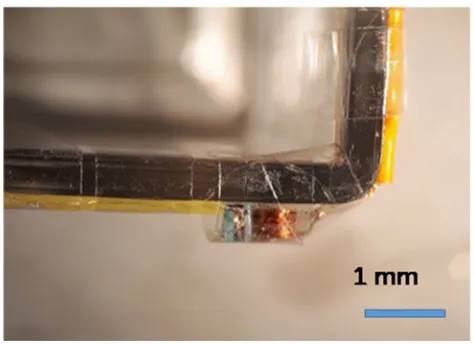
The samples to be measured (RF mapped) are of dimensions well below the regular ID-1 format, with an overall footprint below 50×10 mm, and are constructed in 118µm thick laminate, com-posed of 18µm electrodeposited copper foil laminated to 100µm glass epoxy dielectric substrate. The structuring is performed by means of direct laser lithography. An optical image of the coupling antenna and transponder chip is shown onFigure 1.
The flexible antenna design features 7 turns with outer dimen-sions compatible with applications in devices, such as wristbands and smart wearables. Information storage and communication on the tags is handled by integrated circuit chips, supplied by NXP semiconductor, which have a 69 pF front-end capacitance. The IC is connected across the two antenna terminals by short (<3 mm long) insulated copper wire. Further details on similar assemblies can be found in Ref.3.
The RF magnetic field profiles are measured using a Parker Compumotor©motion control system (seeFig. 2) equipped with Zeta 4-240 microsteppers (x,yandz-axis). The minimum step size is∼10 µm, with a minimum backlash in the range 20-30 µm. A plas-tic support platform of diameter 0.21 m is used as a sample stage; the experimental setup is shown inFigure 4. The minimal separa-tion between the DUT and the RF ground plane is at least 2 cm, and is sufficient to render errors in the absolute signal magnitudes lower than about 10 %.
The DUT is typically affixed to the stage using Kapton™tape (without anti-static coating and therefore magnetic-impurity free).
FIG. 1. Visual image of the RFID tag used as a DUT for the demonstration of the measurement setup capabilities. The regions of the CMOS chip (left), sendust (middle) and copper coils (outside perimeter) are clearly visible.
FIG. 2. Experimental setup for RF scanning using a micro-coil set as inductive sensors positioned within a 0.21 m diameter source coil. (not visible). The DUT is placed under the micro-coil and thez-height adjusted so as to scan as close as possible above the sample surface.Z-scanning or z-slicing can also be performed as an alternative data acquisition strategy.
Thez-height, which is also the separation between the DUT and the measurement coils can be varied, in the range 0 – 25 mm, in order to performz-slicing (to be explored for 3D field reconstruc-tion), but is in most cases kept fixed, as close to the sample surface as possible (∼300-500 µm). An assembly of∼250 µm diameter micro-coils is used for inductive pickup (shown in close-up onFigure 3), in order to measure the integratedz-axis magnetic flux density at a fixed height above the sample surface to a nominal resolution down to 250 µm, The assembly contains four coils – three for the pri-maryx,yand z-components of the magnetic field vector (Bx,By,
Bz)T, and one extra coil purposed for the measurement of the z-axis primary gradient dBz/dzcomponent. The source coil is comprised of 2 turns of 0.5 mm thick copper wire, which are wound around
[image:3.594.310.547.87.250.2] [image:3.594.310.547.474.646.2] [image:3.594.49.285.572.654.2]FIG. 4. Measured (top) 2-D RF profile (in rainbow color scale) of the three orthog-onal field components, generated by the RFID tag, compared to simulated ones (bottom), at the resonance frequency of 13.7 MHz.
[image:4.594.42.541.84.691.2]vided to this source coil using a 50Ω-coupled R&S (ZVB), 4-channel vector network analyzer (10 MHz – 20 GHz). The data acquisition and control routines are written for LabVIEW©6.1. To optimize data acquisition speeds and RF signal-to-noise levels and to pro-vide testing capability up to the nominal specified threshold field intensities of 18 A/m, as required for CLASS 6 PICC, power amplifi-cation is provided using an ENI 411LA model (10 W linear amplifier, 150 KHz - 300 MHz). The acquired data are analyzed and plotted using processing routines written for Mathcad 15©.
III. RESULTS
A set of 2D RF profiles of the field components created by the tag at a frequency of 13.7 MHz (close to resonance) is shown on
Figure 4.
By a direct visual comparison between the experimental pro-files and a set of corresponding computed ones, it becomes clear that there is a very good overall agreement with a simple modelling scheme, where Biot-Savart’s law is used to numerically integrate (using a simple Mathcad code) the field produced by the current distribution in the flat rectangular coils. The only portion of the experimental profiles that is not reproduced sufficiently accurately is in the vicinity of the CMOS chip, which, at this stage, is not included in the simulation model. The majority of the magnetic field is gen-erated by active currents running through the loop antenna, with only a small additional contribution by the eddy (Faucault) currents flowing in the CMOS die.
RF scans of the entire tag antenna area without and with the module are shown in synthetic RGB colour in Figure 5. The figure illustrates that the field is the strongest above the copper coils whether or not sendust flux-concentrator is used. The color scaling is linear and chosen to represent the different spectral regions of the measured data. The R-channel is representing RF-amplitude at 10 MHz, the G-channel at 13 MHz and the B-channel at 16 MHz. In the version where a common colour normalization is performed for the three channels, the clear green overall color of the tag corresponds to the resonance occurring sufficiently close to 13 MHz. The cost for the presence of a sendust flux concen-trator is the increased overall inductance, which down-shifts the resonance frequency to the vicinity of 12 MHz. In further opti-mized designs, this inevitable effect would require the reduction of the number of turns of the copper coil of the tag from 7 to 6, in order to lift the resonance back up, above 13 MHz. Ultimately the best possible compromise depends on the ratio between the mag-netic losses within the flux concentrating material and the resistive losses within the copper loop antenna. Optimization can in princi-ple be considered on both integer and fractional copper-turn basis, by modifying the lateral placement of the CMOS chip over the loop antenna.
Further insight is obtained from the vector field maps of the real and imaginary (in- and out-of-phase) components of the mag-netic field above the tag, at resonance (as shown onFigure 6). As at each spatial point a complete frequency spectrum is obtained exper-imentally, as part of the data post-processing, various cuts and sub-selections, or integrations can be performed, in order to reveal all details available. For example from the frequency-dispersive behav-ior of the real and imaginary parts integrated over a suitable large
FIG. 6. Measured 2-D RF profiles, at resonance, with thexandycomponents of the magnetic field being represented by vector arrows and the primary z -component represented in a rainbow color scheme. The real part (in-phase with the drive field) and the imaginary (out-of-phase with the excitation) are given at the left and right panel, respectively. The dephasing produced by the influence of the CMOS chip is clearly visible. The bottom panel provides detail of the vicinity of the chip in 4D.
[image:5.594.308.547.83.504.2]FIG. 7. 2-D RF profiles (in rainbow colour contrast, with extra directional light sources to visually reveal fine detail) with a sendust inlay (left) and without a sendust inlay (right). The area of the sendust inlay is visible as a darker-blue central region in the left image. Small lat-eral misalignment can be seen between sample remounts. As the pick-up coil assembly is attached onto a transpar-ent support structure, only simple optical alignment with respect to visual mark-ers or features of the DUT has been performed.
conductivity and permittivity of the chip’s body, itself. The real com-ponent (at resonance) reveals the expected ‘stretched’ dipole coil-type profile of the vector directions, quite as if it is sourced with DC equivalent current.
While complex-vector field mapping is revealing the greatest amount of physical information possible, the best signal-to noise ratios for the primary field component is actually achievable by using narrow-band scalar equipment, or equivalent broadband vector sig-nal post-processing of the complete acquired datasets. The results of such a process are demonstrated onFigure 7. Apart from the higher level of spatial and amplitude detail available, there is a strong con-trast advantage to this type of data processing, allowing, for example, for the clear visualization of the flux-concentration properties of
the magnetically-soft sendust region. It becomes apparent that the additional flux concentration is occurring on the expense of the con-traction of flux lines that would have otherwise been located outside the geometrical footprint of the tag. This on its own is advantageous, specifically in cases, where there is a rather limited amount of sur-face area available for occupation by the tag’s loop antenna, such as wristbands, watches and other wearables. Problems do arise, how-ever, in cases where the geometrical overlap between the sendust regions and the coils is not optimized – power is lost in the excita-tion of low-frequency magnetostatic modes of the soft ferromagnet, other than the primary dipole-like one. These higher-order modes are necessarily bringing down the overall projected flux through the loop antenna, thus decreasing the overall geometrical efficiency.
[image:6.594.44.376.85.301.2] [image:6.594.41.556.476.708.2]demonstrated inFigure 8, as measured at the point of highest RF field close to the geometrical middle of the module’s area. This is possible, in principle, for an arbitrary spatial point, as complex spec-tral data is recorded for each spatial point and each component of the magnetic field vector. Apart from a few artifacts related to minor resonances within the broadband power amplifier used in the mea-surements, the scalar transmission spectrum (as seen by the micro-pickup coils) corresponds to the combined resonance of the antenna (the inductor) and the chip (the capacitor). Both vector components can be explicitly fitted (using non-linear least-squares regression procedures) to either a Lorentzian or a derivative Lorentzian disper-sion. A further linear background correction accounts for the direct-mutual inductance between the pick-up and source coils. These resonance characteristics are in good agreement with the experi-mental data, only if a second set of much broader resonances is introduced as shown onFigure 8. The two slightly offset resonance frequencies are 13.7 and 14.2 MHz, and are believed to be a result of the frequency-dispersive magnetic permeability of the sendust inlay.
IV. CONCLUSIONS
It has been demonstrated by actual experimental RF scanning maps of the complex vector magnetic field components’ spectra in the vicinity of RFID tags, that the detailed spatial, and frequency-dispersive information made available, allows for detailed compari-son, between experiment and various modelling schemes, including finite element calculations and bulk effective circuit theory. Direct
concentrators onto the tags, allowing for much improved geomet-rical and material design choices to be made, gaining overall RFID system performance and reducing material costs.
Such field mapping strategy, as demonstrated here, can be read-ily integrated into a variety of industrial testing environments con-cerned with HF, UHF and microwave mapping, such as financial payment cards production facilities and development laboratories for contactless payment jewelry and wristbands, among others.
ACKNOWLEDGMENTS
The use of common equipment within the CRANN-AMBER centre (SFI/12/RC/2278), Trinity College Dublin, is gratefully acknowledged, as is co-funding by Science Foundation Ireland.
REFERENCES
1
V. Chawla and D. S. Ha, “An overview of passive RFID,”IEEE Commun. Mag. 45(9), 11–17 (2007).
2Identification cards Contactless integrated circuit(s) cards Proximity cards -Part 1: Physical characteristics, ISO/IEC 14443-1, 2000; -Part 2: Radio frequency power and signal interface, ISO/IEC 14443-2, 2010; Part 3: Initialization and anticollision, ISO/IEC 14443-3, 2011; Part 4: Transmission protocol, ISO/IEC 14443-4, 2008.
3Smartcard with coupling frame and method of increasing activation distance of a transponder chip module, by D. Finnet al.(2014, Dec 11), Patent US20140361086 [Online], Available:http://www.google.com/patents/US20140361086.