COMMUNICATION
Cite this:Nanoscale, 2018,10, 17557
Received 14th March 2018, Accepted 6th June 2018 DOI: 10.1039/c8nr02134a
rsc.li/nanoscale
Optimized single-layer MoS
2
fi
eld-e
ff
ect
transis-tors by non-covalent functionalisation
†
HyunJeong Kim,
‡
a,bWungYeon Kim,
‡
a,bMaria O
’
Brien,
aNiall McEvoy,
aChanyoung Yim,
cMario Marcia,
dFrank Hauke,
dAndreas Hirsch,
dGyu-Tae Kim
band Georg S. Duesberg
*
a,cField-effect transistors (FETs) with non-covalently functionalised molybdenum disulfide (MoS2) channels grown by chemical vapour
deposition (CVD) on SiO2 are reported. The dangling-bond-free
surface of MoS2 was functionalised with a perylene bisimide
derivative to allow for the deposition of Al2O3 dielectric. This
allowed the fabrication of top-gated, fully encapsulated MoS2
FETs. Furthermore, by the definition of vertical contacts on MoS2,
devices, in which the channel area was never exposed to polymers, were fabricated. The MoS2FETs showed some of the highest
mobi-lities for transistors fabricated on SiO2with Al2O3as the top-gate
dielectric reported so far. Thus, gate-stack engineering using inno-vative chemistry is a promising approach for the fabrication of reliable electronic devices based on 2D materials.
Introduction
Following the advent of graphene,1 two-dimensional (2D) materials have been extensively examined as promising materials for nanoelectronics.2–5 Unlike graphene, in which the absent bandgap limits its applications,6–92D semiconduct-ing transition-metal dichalcogenides (TMDs), such as MoS2,
are considered as promising materials for future nanoelectro-nic devices.10–14 To date, several methods have been intro-duced to obtain TMDs, each with benefits and drawbacks: mechanical exfoliation delivers high-quality flakes10,15 but suffers from scalability, while liquid-phase exfoliated materials have limited device performance.16–19Additionally, exfoliation
leads to dispersed layer thicknesses, which give rise to varying properties.15,20–22Thermally assisted conversion (TAC) of
pre-deposited metals or metal oxides yields a variety of large-scale TMD films with a controllable thickness, however they are typi-cally polycrystalline and defective.23–25Chemical vapour
depo-sition (CVD) produces high-quality TMD crystals of predomi-nantly monolayer thickness, however the growth of continu-ous, large-area films remains a challenge.26–28 Given the
associated advantages, CVD growth is the most suitable method for scalable fabrication of industry-relevant electronic devices.
Besides the challenges in synthesis, one of the major issues in the fabrication of reliable devices with monolayer TMDs is the control over the surface chemistry. Due to their monolayer nature, the properties of 2D materials depend strongly on the environment. Adsorbates lead to doping via charge transfer, resulting in significant changes in the electrical properties. This effect is exploited in chemiresistors or ChemFETs for chemical sensing.29,30Furthermore, most monolayer TMDs are
unstable and degrade under ambient conditions due to oxi-dation by water and/or oxygen.31,32This leads to a deteriorated
performance of FETs due to hysteresis and undefined doping. Therefore, it is important to passivate the 2D channels of devices for their stable operation. High-κ materials are con-sidered to be excellent passivation layers and gate insulators. In general, they are suitable for low leakage and low power logic devices due to the high dielectric constant.33
Furthermore, high-κmaterials improve the carrier mobility by reducing Coulomb scattering for nanostructures34or
increas-ing the effective gate electric field.35Al
2O3is one of the most
commonly used high-κ materials, often deposited using tri-methylaluminum (TMA, Al(CH3)3) and an oxidation agent,
water or ozone, by atomic layer deposition (ALD). However, the basal planes of 2D nanosheets, such as graphene or MoS2, do
not react with TMA due to the lack of dangling bonds or surface hydroxyl groups.36–39Thus, the formation of a seeding
layer is required to perform ALD on the clean surface of 2D van der Waals crystals. We have shown that when perylene bis-imides are deposited from the liquid phase onto graphene,
†Electronic supplementary information (ESI) available. See DOI: 10.1039/ c8nr02134a
‡These authors contributed equally to this work.
aCRANN&AMBER Centres and School of Chemistry, Trinity College Dublin, Dublin 2,
Ireland. E-mail: [email protected]
bSchool of Electrical Engineering, Korea University, Seoul 02841, South Korea
cInstitute of Physics, EIT 2, Faculty of Electrical Engineering and Information
Technology, Universität der Bundeswehr München, 85577 Neubiberg, Germany dChair of Organic Chemistry II, Friedrich-Alexander University of Erlangen-Nürnberg,
Nikolaus Fiebiger Str. 10, 91058 Erlangen, Germany
Open Access Article. Published on 18 September 2018. Downloaded on 7/23/2019 11:18:00 AM.
This article is licensed under a
Creative Commons Attribution 3.0 Unported Licence.
they form self-assembled monolayers (SAMs).40,41Specifically, –COOH and –OH units of the molecule react with TMA and promote the nucleation.33,42,43The same non-covalent functio-nalisation route was adopted for TMD layers,44 wherein the perylene bisimide functional layer served as a stable seeding layer for Al2O3depositionviaALD.
In this study we fabricated top-gated FETs with functiona-lised CVD-grown MoS2. The perylene bisimide functional layer
is used as a seeding layer for Al2O3 deposition, fabricating
fully encapsulated MoS2FETs. We compared the devices
fabri-cated by two different process flows. In both cases the electri-cal integrity of the TMD is maintained. Furthermore, the influ-ence of the polymer residue on the device performance could be quantified.
Methods
MoS2growth
MoS2samples were grown in a micro-cavity in a two-zone CVD
furnace at 700 °C as described previously.26The samples were grown directly on SiO2/Si (300 nm thick SiO2, highly p-doped
Si) substrates with MoO3and sulfur as solid precursors.
Device fabrication
Back-gated MoS2FETs.The source/drain electrodes on MoS2
flakes were patterned by electron beam lithography (EBL), with an electron beam resist (PMMA–A4, MicroChem) which was spin-coated onto the sample. EBL was performed using a Zeiss Supra 40 with a Raith EBL kit. After baking at 180 °C and developing with a MIBK : IPA (1 : 3) solution, the metal electro-des (Ti/Au, 5 nm/50 nm) were deposited by sputtering using a Gatan Precision Etching and Coating System (PECS).
Top-gated MoS2FETs type 1.Directly after the MoS2growth,
perylene bisimide dissolved in aqueous buffer solution was de-posited on the sample. Source/drain electrodes were defined by EBL as described above. The metal electrodes (Ti/Au, 5 nm/ 50 nm) were deposited by using an electron beam evaporator (Temescal FC-2000). After lift-off, a 34 nm thick Al2O3layer was
then deposited on the MoS2channel region which was defined
by EBL, using ALD (TP01, ATV Technology) with TMA and H2O
precursors at 80 °C. The Al2O3 thickness was measured by
atomic force microscopy (AFM) as shown in Fig. S1(a).† Finally, the top-gate metal electrode (Ti/Au, 5 nm/50 nm), pat-terned by EBL, was sputtered (Gatan Precision Etching and Coating System).
Top-gated MoS2FETs type 2.Directly after the MoS2growth,
perylene bisimide dissolved in aqueous buffer solution was de-posited on the MoS2. Subsequently, a 16 nm thick Al2O3layer
was deposited onto the samples by ALD at 80 °C with TMA and H2O as precursors. The height profile of the first
ALD-grown Al2O3layer measured by AFM is shown in Fig. S1(b).†
PMMA (A4, MicroChem) was then spin-coated on the Al2O3
layer and source/drain electrodes were defined by EBL. After development, the exposed Al2O3layer was removed with 2.38%
tetramethylammonium hydroxide (TMAH) solution in H2O at
55 °C, creating a vertical contact hole (VIA). Then metal elec-trodes (Ti/Au, 5 nm/50 nm) were deposited by electron beam evaporation, followed by lift-off. In order to prevent the poss-ible leakage of the gate dielectrics during electrical measure-ments, an additional 24 nm thick Al2O3 was deposited onto
the gate region. The AFM height profile of the second ALD Al2O3thickness is shown in Fig. S1(c).†In a subsequent step,
the top gate electrode was defined by EBL and the gate metal electrode (Ti/Au, 5 nm/50 nm) was sputtered, followed by lift-off.
Raman spectroscopy was performed using LabRam ARAMIS IR2 (HORIBA JOBIN YVON) and a WITec Alpha 300R with a 532 nm laser as the excitation source. The thicknesses of Al2O3
and MoS2 were measured using AFM (MFP-3D, Asylum
Research). The topographic images of the MoS2 surface were
obtained by AFM (Park Systems Park XE100). Scanning elec-tron microscopy (SEM) imaging was done using a MIRA3 (TESCAN). Electrical measurements were conducted on a JANIS probe station connected to a Keithley 2612A source meter unit under vacuum (top-gated FETs: ∼3.7 Torr, back-gated FETs: ∼2.3 × 10⁻⁴ Torr) at room temperature. The sub-strate was connected to the ground during the electrical measurement of the top-gated FETs.
Results
The CVD growth yields randomly distributed, monolayer MoS2
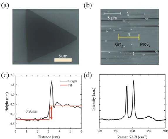
regions, e.g.flakes, which are mostly triangular in shape and extend over several micrometers. In Fig. 1 typical results of CVD-grown MoS2 on SiO2 are presented. In Fig. 1(a) a SEM
image of the triangular shaped MoS2is shown. AFM
measure-ments confirmed the monolayer nature of the triangular regions, as shown in Fig. 1(b) and (c). A Raman spectrum of an as-grown MoS2flake is shown in Fig. 1(d), the in-plane (E′) and
out-of-plane (A′1) peaks occur at 383 and 403 cm−1,
respect-ively, which is consistent with monolayered MoS2. Some
bilayer and/or multilayer formation also can take place in the seeding regions of the flakes as shown in the inset of Fig. 2(a) (line region of the optical image).
To reveal the electrical properties of the CVD-grown MoS2,
flakes were brought into contact with EBL-defined electrodes as shown in Fig. S2(a).†Using the substrate as the back gate, a FET with an MoS2 channel was defined as schematically
shown in the inset of Fig. S2(a).†The FET shows on/offratios on the order of 103, and the average field-effect mobility of the device is 0.66 cm2V−1s−1for forward sweep and 0.79 cm2 V−1s−1for reverse sweep. These relatively low mobility values can be attributed to the scattering of carriers at the surface and the SiO2 substrate.45 In order to improve the
perform-ance, FETs in which the MoS2 channel is encapsulated and
the channel has a top-gate electrode, separated by a high-κ oxide for effective modulation, can be fabricated. The gate dielectric deposition is ideally realised in a non-destructive and scalable manner by ALD. However, generally ALD on clean 2D van der Waals materials is challenging, due to the
Communication Nanoscale
Open Access Article. Published on 18 September 2018. Downloaded on 7/23/2019 11:18:00 AM.
This article is licensed under a
Creative Commons Attribution 3.0 Unported Licence.
absence of seeding sites such as hydroxyl or carbonyl oxides.39,46–48
AFM measurements were carried out to investigate the Al2O3deposition on MoS2. As also shown in Fig. 2 the
triangu-lar MoS2 flakes consist of monolayers. There is some double
and multilayer formation in the seeding region at the centre of the grain as shown in the inset of Fig. 2(a) (line region). Fig. 2(a) shows an AFM topography image of an ALD-Al2O3
layer deposited on a MoS2flake with 45 cycles of TMA/H2O at
80 °C. Fig. 2(c) shows the line profile of the yellow line in Fig. 2(a). The step height between the monolayer and substrate is approximately 0.34 nm. The MoS2lies on average lower than
the SiO2 substrate, and the monolayer surface is very rough.
This is attributed to the inhomogeneous and imperfect depo-sition of Al2O3on the monolayer. Evidently, on the monolayer
MoS2 some Al2O3island growth has taken place, but no
con-Fig. 1 (a) SEM image of CVD-grown MoS2. (b) AFM topography of CVD-grown MoS2. (c) Average line profile along the marked line in (b). The step
height between theflake and substrate is∼0.7 nm, confirming the monolayer nature of the triangular regions. (d) Raman spectrum of monolayer CVD-grown MoS2.
Fig. 2 (a) AFM topography of pristine MoS2after Al2O3deposition by ALD. A very rough surface due to Al2O3islands can be seen on the MoS2
regions. Inset: Optical image of the investigated region. (b) AFM topography of MoS2functionalized with perylene bisimide after Al2O3deposition by
ALD. Inset: Optical image of the investigated region. (c) Line profile along the marked line in (a). The MoS2lies on average lower than that in the SiO2
substrate. (d) Line profile along the marked line in (b). The MoS2lies higher than that in the SiO2substrate.
Open Access Article. Published on 18 September 2018. Downloaded on 7/23/2019 11:18:00 AM.
This article is licensed under a
[image:3.595.154.441.47.284.2] [image:3.595.89.444.343.547.2]tinuous, complete coverage is reached. The step height between the multilayer and substrate is approximately 1.3 nm, and this is close to the thickness of bilayer MoS2. This
indi-cates that in the multilayer region Al2O3 growth took place.
Also, Al2O3 deposition can be seen at the edges of the
mono-layer MoS2 flakes resulting in a high step at the edge of the
MoS2flake. This is attributed to a higher abundance of reactive
sites such as dangling bonds and defects at the edges of the MoS2 layers acting as anchor sites for the deposition of
Al2O3.44 Fig. 2(b) shows an AFM topography image of an
ALD-Al2O3 layer on a perylene bisimide-covered MoS2 flake
with 45 cycles of TMA/H2O at 80 °C. In contrast to Fig. 2(a),
the Al2O3–MoS2surface in Fig. 2(b) is uniform and lies higher
than the SiO2substrate. Thus, the perylene bisimide layer acts
as a seed for ALD growth, resulting in a homogenous and con-tinuous Al2O3 layer. Fig. 2(d) shows the line profiles of
Fig. 2(b) from the MoS2flake to the substrate. The step height
between the monolayer and substrate is approximately 1.75 nm, and this exceeds the monolayer thickness. The additional thickness is attributed to the perylene bisimide layer. Thus, the perylene bisimide functionalisation allows the ALD of dielectrics on clean dangling-bond-free TMD surfaces.
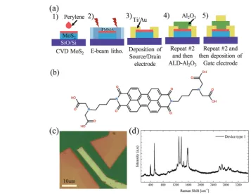
Having optimized the dielectric deposition, we investigated the viability of our non-covalent functionalisation to optimize the gate-stack formation of 2D material FETs. The process flow to yield fully encapsulated top-gated MoS2FETs (device type 1)
is shown in the schematic in Fig. 3(a). It follows the standard device fabrication processes with E-Beam resist (PMMA) depo-sition directly onto the whole substrate; however in our case
the PMMA was deposited after the deposition of perylene bis-imide (Fig. 3(b)). Source/drain electrodes were patterned by EBL and deposited by evaporation. After lift-off, the Al2O3gate
dielectric was deposited on the entire MoS2 channel region
defined by EBL. This was followed by the deposition of the top gate electrode, after another lithographic step. An optical image of one device is shown in Fig. 3(c). Raman spectroscopy was used to confirm the presence of the MoS2monolayer and
perylene SAM after the completion of the gate stack. Fig. 3(d) shows the peaks at positions at∼384 cm−1 and 401 cm−1for the completed device, corresponding to the E′and A’1 modes
of MoS2, respectively. Furthermore, the spectra exhibit several
peaks in the region of 1300 cm−1to 1600 cm−1typical of peryl-ene bisimide. This underlines the remarkable stability of the perylene SAM, and it withstands the polymer removal with acetone and the ALD process.
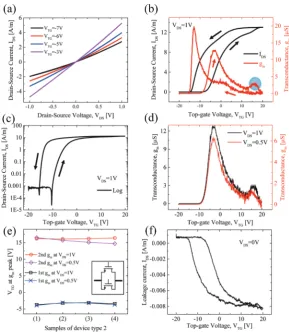
Fig. 4(a) shows theIDS–VDSoutput characteristics at various
top-gate voltages (VTG) of device type 1. The SiO2substrate of
the device was grounded during all measurements, reducing the possible capacitive coupling between top- and back-side dielectrics.49 Linear behavior is observed at each VTG, which
indicates that the integration route yields good contacts and that the perylene bisimide layer does not significantly affect the contact properties between MoS2 and the electrodes.
Fig. 4(b) shows the typical IDS–VGS transfer characteristics of
device type 1. This exhibits a counter clockwise hysteresis. The reverse sweep of the top-gate voltage, VTG, exhibits a higher
conductivity compared with the forward sweep of VTG. The
counter clockwise hysteresis can be attributed to the positive
Fig. 3 Top-gated MoS2FET type 1: (a) Schematic of the processflow. (b) Chemical structure of the perylene bisimide derivative. (c) Top view optical
image of the fully fabricated device. (d) Raman spectrum of the channel area of a fully fabricated device.
Communication Nanoscale
Open Access Article. Published on 18 September 2018. Downloaded on 7/23/2019 11:18:00 AM.
This article is licensed under a
Creative Commons Attribution 3.0 Unported Licence.
[image:4.595.86.444.417.693.2]mobile charges in Al2O3.50,51In the forwardVTGsweep,
posi-tive mobile charges in Al2O3 move to the Al2O3/( perylene
bis-imide)/MoS2 interface. In the reverse VTG sweep, the positive
mobile charges located near the MoS2 surface induce an
additional electrical field, and this leads to a lower threshold voltage (VTH) and increases the current. Additionally, we
com-pared the transfer characteristics between two back-gated MoS2FETs, with and without a perylene bisimide layer on the
MoS2 channels. As shown in Fig. S2(c) and (f ) of the ESI,†
both devices show a similar hysteresis trend, indicating that the perylene bisimide layer does not play an important role in the observed hysteresis. Sub-threshold swing is 283 mV per decade for the forward sweep and 214 mV per decade for the reverse sweep. The field-effect mobility (μFE) is calculated by the transfer characteristic using the following equation:
μFE¼
Lgm
WCAl2O3VDS
ð1Þ
where CAl2O3 denotes gate dielectric capacitance, gm denotes
transconductance,VDSdenotes drain–source voltage,Ldenotes
channel length, and W denotes channel width. The channel shape does not often correspond to a rectangle, and thus the channel width is obtained by dividing the total channel area by the channel length. TheμFEof the device is 21.4 cm2 V−1 s−1for the forward sweep and 33.4 cm2V−1s−1for the reverse sweep. The red line in Fig. 4(b) indicates thegmof the device.
The slope of drain/source current significantly increases until thegmreaches a peak, and then decreases whenVTGincreases.
However, the device exhibits an intriguing secondgmpeak for
the forwardVTGsweep (blue-circled region) which is consistent
with a small hump in the transfer characteristics at the same
VTG. Such a secondgmpeak was also observed at variousVDS
(Fig. 4(d)) in four out of five samples. Interestingly, as shown in Fig. 4(e), the secondgmpeak appears at similarVTG(∼16 V)
in all four samples regardless ofVDS, indicating that there is a
common reason for the secondgmpeak with reproducibility.
Similar signatures in the transfer characteristics were observed in SOI MOSFETs,52–56polysilicon thin film transistors,57and gate injection GaN-based transistors.58Even in the case of the previous studies of SOI MOSFETs, which are more optimized than the MoS2 FETs studied here, the origin of additional
Fig. 4 Electrical characterisation of device type 1: (a) Output characteristics. (b) Transfer characteristics (black line) and transconductance (red line) curves for various top-gate voltages atVDS= 1 V. The blue circle highlights the second transconductance peak. (c) Logarithmic plot of transfer
characteristics. (d) Transconductance curves atVDS= 0.5 V (red line) and 1 V (black line). (e) Top-gate voltages for thefirst and second
transconduc-tance peaks of type 1 devices atVDS= 0.5 V and 1 V. Inset: equivalent circuit model with two transistors connected in parallel. (f ) Plot of leakage
currentversustop-gate voltage.
Open Access Article. Published on 18 September 2018. Downloaded on 7/23/2019 11:18:00 AM.
This article is licensed under a
[image:5.595.152.442.47.380.2]transport carriers varied depending on the device structure and materials. Thus, the origin of the secondgmpeak cannot
be exactly determined at this stage. However, as shown in Fig. 4(b), a slight increase in current was observed at VTG of
the secondgmpeak. As discussed in previous studies,52–58the
injection of additional transport carriers could be considered as one of the reasons for the secondgm peak. In the case of
device type 1, the leakage current (see Fig. 4(f )), obtained by measuring theIDSatVDS= 0 V under aVTGsweep, can be ruled
out as a source of the additional carriers, since it is too low to affect the transfer characteristics. The devices can be expressed using an equivalent circuit model, composed of a main tran-sistor connected to a parasitic trantran-sistor in parallel, as shown in the inset of Fig. 4(e). In the equivalent circuit model, the threshold voltage of the main transistor differs from that of the parasitic transistor. The second gm peak value is small
compared to the firstgmpeak, as shown in Fig. 4(b). This is
because the current generated after the parasitic transistor turns on is low.
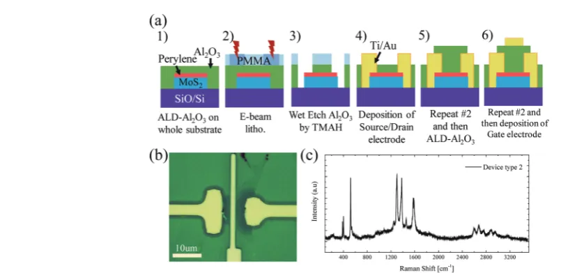
A second more advanced process flow avoiding any contact of the channel region with the polymer resist was developed. As shown in Fig. 5(a), for device type 2 we deposited the Al2O3
layer on the whole substrate directly after perylene bisimide
functionalisation. The source/drain electrodes were patterned by EBL, effectively creating contact holes by wet etching of the Al2O3layer with an etch stop on the MoS2. This realisation of
vertical interconnects (VIAs) with metal evaporation to contact 2D materials is an important step in their successful inte-gration. Importantly, this process flow has an advantage that the MoS2 channel is never in contact with the polymer resist.
The presence of perylene between the Al2O3and the MoS2was
confirmed by using Raman spectroscopy. The spectra were obtained after device fabrication was completed. Like device type 1, the typical signatures for MoS2 at ∼385 cm−1 and
405 cm−1and perylene at 1300 cm−1to 1600 cm−1are observed as shown in Fig. 5(c).
In Fig. 6(a), the output characteristics of device type 2 are shown. They exhibit a linear behavior like device type 1, indi-cating that the contacts between the monolayer MoS2and
elec-trodes, which were defined by VIA etching and filling, were well established. This is an important achievement for the integration of 2D materials. Fig. 6(b) shows the transfer charac-teristics and transconductance of the device. A counter clock-wise hysteresis appears, similar to the device type 1. Sub-threshold swing is 255 mV per decade for the forward sweep and 224 mV per decade for the reverse sweep. The μFE of
Fig. 5 Top-gated MoS2FET type 2: (a) Schematic of the processflow. (b) Top view optical image of the fully fabricated device. (c) Raman spectrum
of the channel area of a fully fabricated device.
Fig. 6 Electrical characterisation of device type 2: (a) output characteristics. (b) Transfer characteristics (black line) and transconductance (red line) for various top gate voltages atVDS= 1 V. (c) Logarithmic plot of transfer characteristics.
Communication Nanoscale
Open Access Article. Published on 18 September 2018. Downloaded on 7/23/2019 11:18:00 AM.
This article is licensed under a
Creative Commons Attribution 3.0 Unported Licence.
[image:6.595.46.454.353.549.2] [image:6.595.143.448.602.694.2]device was extracted to be 22 cm2 V−1 s−1 for the forward sweep and 48.7 cm2 V−1 s−1 for the reverse sweep. Unlike device type 1, the secondgmpeak was not observed in device
type 2, as shown with a red line in Fig. 6(b).
The main difference between device type 1 and 2 is that in the latter case the functionalized MoS2 channel was not in
contact with the resist during the fabrication. It is well known that resist residues can remain on the film surface after devel-opment and lift-off processes. To investigate this, the MoS2
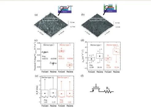
surface was characterized by AFM during fabrication. Fig. 7(a) shows the functionalized MoS2surface after the development
of the polymer resists during the fabrication of device type 1 (step 2 in Fig. 3(a)). A relatively rough surface with a root-mean-square (RMS) roughness of 0.54 nm was observed. This roughness is likely due to polymer residues which remain in the channel area. In contrast, the functionalized MoS2surface
after wet-etching of the contact area (step 3 in Fig. 5(a)) of the device type 2 appears to be relatively flat (RMS roughness = 0.30 nm). Both the RMS and average values of the surface roughness of device type 1 clearly exceed those of device type
2. Thus one can deduce that while type 1 devices have polymer residues on the surface of the channel, type 2 devices have a relatively clean interface to the top gate dielectric. Thus we can tentatively attribute the secondgmpeak to the polymer residue
in the channel area in device type 1, however additional experi-ments are required to analyze the exact mechanisms that cause the secondgmpeak.
To investigate the influence of resist residues on the device performance, five samples were fabricated and compared for each device type. The threshold voltage, mobilities and contact resistances of the devices are summarized in Fig. 7(c), (d) and (e). Device type 1 (34 nm) and 2 (40 nm) have different Al2O3
thicknesses. Even when applying the same gate voltage, the gate electric field is different depending on the dielectric thick-ness. While considering the gate electric field, the threshold voltage was multiplied byCAl2O3. As shown in Fig. 7(c), the
hys-teresis (VTH,reverse–VTH,forward) of device type 2 (0.0235 V F m−1)
increased by 26% compared to device type 1 (0.0187 V F m−1). During the second deposition of Al2O3of device type 2,
inter-face states would form between the first and second ALD-Al2O3
Fig. 7 AFM images of the device type 1 (a) and device type 2 (b) prior to the deposition of the source–drain electrode. (c) Threshold voltage multi-plied byCAl2O3, (d)field-effect mobilities and (e) contact resistance multiplied by the channel width. Distributions offive samples of device type 1
(black) and device type 2 (red) for theVTGsweep directions. Open triangles denote the data for each sample. Filled squares denote the average of
five samples. Boxes correspond to the standard error of samples. (f ) Equivalent circuit with a serial resistor connected to the transistor. Contact re-sistance is extracted by using this model.
Open Access Article. Published on 18 September 2018. Downloaded on 7/23/2019 11:18:00 AM.
This article is licensed under a
[image:7.595.47.540.314.662.2]layers and the overall quality of the Al2O3 of device type 2
would get worse, leading to large hysteresis compared to device type 1. As shown in Fig. 7(d), the averageμFEof device type 1 is lower than that of device type 2. In particular, the average μFE of the device type 2 (32.3 cm2 V−1 s−1) for the reverse sweep increased by 61% compared to device type 1 (20.1 cm2 V−1 s−1). This can be tentatively assigned to the increased surface roughness and remote charge scattering. As shown in Fig. 7(a), the functionalized MoS2 surface of device
type 1 has resist residues in the channel area, unlike device type 2. Even though the resist residues may not directly adhere to MoS2due to the perylene SAM, it can increase the surface
roughness and act like a fixed charge inside the gate stack. This latter disturbance can cause scattering by remote surface scattering.59,60Further studies are needed to understand why theμFEof both device types is more pronounced in the reverse sweep than in the forward sweep in Fig. 7(d). The effect of resist residues on the contact resistance of the device was also investigated. As shown in Fig. 7(e), in the highVTG region in
Fig. 4(b) and Fig. 6(b), the current is saturated due to the influ-ence of contact resistance (Rs).Rsis extracted by using an
equi-valent circuit model with a resistor serially connected to the transistor as shown in Fig. 7(f ).Rs is obtained by using the
graphical method61and the following equation:
IDS¼μFECox
W
L ðVTGVTHÞðVDSIDSRsÞ
1
2ðVDSIDSRsÞ 2
ð2Þ
AtVDS= 1 V,Rs along each sweep direction was calculated
by using the transfer characteristics. Different channel widths (W) were considered for each device, and the width was multi-plied byRs. The distribution of theRsWof device type 1 and 2
is shown in Fig. 7(e). The averageRsWof device type 2 (0.95
Ωm) for forward sweep reduced by 8% compared to device type 1 (1.03 Ωm), and the averageRsWof device type 2 (1.02
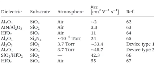
Ωm) for reverse sweep reduced by 11% compared to device type 1 (1.15 Ωm). This strongly suggests that the absence of polymer residues in the source and drain contact regions reduces the contact resistance, but the effect of polymer resi-dues on mobility exceeds that of the contact resistance. In Table 1 the best mobilities for various top-gated FETs with CVD-grown MoS2 channels are listed. Compared to literature
values our best device type 2 exhibits the second highest
mobi-lity reported so far. Thus the process flows with perylene bisi-mide functionalisation can be suggested as a viable route for MoS2integration, leading to reliable dielectric deposition with
reproducible results and high mobilities.
Conclusion
In this study, top-gated FETs with CVD-grown MoS2were
fabri-cated. A non-covalent perylene bisimide functionalization was used to facilitate ALD of Al2O3as a dielectric and passivation
layer. Perylene bisimide was simply deposited on MoS2 by
drop-casting at room temperature. Furthermore, we were able to define vertical contacts to the MoS2channels, yielding
fully-encapsulated MoS2 FETs. Perylene bisimide was
non-destruc-tively attached to MoS2 and led to improved device
perform-ance as revealed by surface characterization and electrical measurements. The field-effect mobility for the MoS2 FETs
was found to be 48.7 cm2V−1s−1, which is the second highest among top-gated CVD MoS2FETs on SiO2substrates, and the
highest with Al2O3 as the top-gate dielectric reported so far.
Thus our work suggests that non-covalent functionalisation is a viable strategy to fabricate devices with monolayer 2D materials. Additionally, we investigated the effect of resist resi-dues on the field-effect mobility and contact resistance. This study represents a significant step towards the fabrication of reproducible TMD-based devices, with interface engineering for passivation and dielectric deposition and contact for-mation as well as better understanding of the effects of polymer residues.
Con
fl
icts of interest
There are no conflicts to declare.
Acknowledgements
The authors wish to thank Dr Sojeong Park and Dr Christian Wirtz. This research is supported by the National Research Foundation of Korea – Ministry of Science and ICT (NRF-2017M3A7B4049119) and by the Multi-Ministry Collaborative R&D Program through the National Research Foundation of Korea funded by KNPA, MSIT, MOTIE, ME, and NFA (NRF-2017M3D9A1073924). We further acknowledge the support from the Science Foundation Ireland (SFI) for grants 15/ SIRG/3329, 12/RC/2278 and 15/IA/3131, and the European Union Seventh Framework Program under Graphene Flagship, 604391 and 785219.
References
1 K. S. Novoselov, A. K. Geim, S. V. Morozov, D. Jiang, Y. Zhang, S. V. Dubonos, I. V. Grigorieva and A. A. Firsov,
[image:8.595.41.291.616.721.2]Science, 2004,306, 666–669. Table 1 Summary of reported effective mobilities for the top-gated
CVD MoS2FETs
Dielectric Substrate Atmosphere
μFE
[cm2V−1s−1] Ref.
Al2O3 SiO2 Air ∼2 62 AIN/Al2O3 SiO2 Air 3.3 63 HfO2 SiO2 Air 11 64 Al2O3 Si3N4 ∼10−6Torr 24 65
Al2O3 SiO2 3.7 Torr ∼33.4 Device type 1 Al2O3 SiO2 3.7 Torr ∼48.7 Device type 2 SiO2/HfO2 SiO2 — 42.3 66
HfOx SiO2 Air 55 67
Communication Nanoscale
Open Access Article. Published on 18 September 2018. Downloaded on 7/23/2019 11:18:00 AM.
This article is licensed under a
Creative Commons Attribution 3.0 Unported Licence.
2 Editorial,Nat. Mater., 2017,16, 155–155.
3 D. Akinwande, N. Petrone and J. Hone, Nat. Commun., 2014,5, 5678.
4 F. H. L. Koppens, T. Mueller, P. Avouris, A. C. Ferrari, M. S. Vitiello and M. Polini, Nat. Nanotechnol., 2014, 9, 780–793.
5 G. Fiori, F. Bonaccorso, G. Iannaccone, T. Palacios, D. Neumaier, A. Seabaugh, S. K. Banerjee and L. Colombo,
Nat. Nanotechnol., 2014,9, 768–779.
6 B. Guo, Q. Liu, E. Chen, H. Zhu, L. Fang and J. R. Gong,
Nano Lett., 2010,10, 4975–4980.
7 D. Wei, Y. Liu, Y. Wang, H. Zhang, L. Huang and G. Yu,
Nano Lett., 2009,9, 1752–1758.
8 X. Li, X. Wang, L. Zhang, S. Lee and H. Dai,Science, 2008, 319, 1229–1232.
9 M. Y. Han, B. Özyilmaz, Y. Zhang and P. Kim, Phys. Rev. Lett., 2007,98, 206805.
10 B. Radisavljevic, A. Radenovic, J. Brivio, V. Giacometti and A. Kis,Nat. Nanotechnol., 2011,6, 147–150.
11 A. Splendiani, L. Sun, Y. Zhang, T. Li, J. Kim, C.-Y. Chim, G. Galli and F. Wang, Nano Lett., 2010, 10, 1271– 1275.
12 B. Radisavljevic, M. B. Whitwick and A. Kis, ACS Nano, 2011,5, 9934–9938.
13 Y. Yoon, K. Ganapathi and S. Salahuddin,Nano Lett., 2011, 11, 3768–3773.
14 L. Yu, D. El-Damak, U. Radhakrishna, X. Ling, A. Zubair, Y. Lin, Y. Zhang, M.-H. Chuang, Y.-H. Lee, D. Antoniadis, J. Kong, A. Chandrakasan and T. Palacios,Nano Lett., 2016, 16, 6349–6356.
15 K. F. Mak, C. Lee, J. Hone, J. Shan and T. F. Heinz, Phys. Rev. Lett., 2010,105, 136805.
16 J. N. Coleman, M. Lotya, A. O’Neill, S. D. Bergin, P. J. King, U. Khan, K. Young, A. Gaucher, S. De, R. J. Smith, I. V. Shvets, S. K. Arora, G. Stanton, H.-Y. Kim, K. Lee, G. T. Kim, G. S. Duesberg, T. Hallam, J. J. Boland, J. J. Wang, J. F. Donegan, J. C. Grunlan, G. Moriarty, A. Shmeliov, R. J. Nicholls, J. M. Perkins, E. M. Grieveson, K. Theuwissen, D. W. McComb, P. D. Nellist and V. Nicolosi,Science, 2011,331, 568–571.
17 C. Backes, R. J. Smith, N. McEvoy, N. C. Berner, D. McCloskey, H. C. Nerl, A. O’Neill, P. J. King, T. Higgins, D. Hanlon, N. Scheuschner, J. Maultzsch, L. Houben, G. S. Duesberg, J. F. Donegan, V. Nicolosi and J. N. Coleman,Nat. Commun., 2014,5, 4576.
18 K. Lee, H.-Y. Kim, M. Lotya, J. N. Coleman, G.-T. Kim and G. S. Duesberg,Adv. Mater., 2011,23, 4178–4182.
19 A. G. Kelly, T. Hallam, C. Backes, A. Harvey, A. S. Esmaeily, I. Godwin, J. Coelho, V. Nicolosi, J. Lauth, A. Kulkarni, S. Kinge, L. D. A. Siebbeles, G. S. Duesberg and J. N. Coleman,Science, 2017,356, 69–73.
20 J. Kwon, J.-Y. Lee, Y.-J. Yu, C.-H. Lee, X. Cui, J. Hone and G.-H. Lee,Nanoscale, 2017,9, 6151–6157.
21 S.-L. Li, K. Wakabayashi, Y. Xu, S. Nakaharai, K. Komatsu, W.-W. Li, Y.-F. Lin, A. Aparecido-Ferreira and K. Tsukagoshi,Nano Lett., 2013,13, 3546–3552.
22 M.-W. Lin, I. I. Kravchenko, J. Fowlkes, X. Li, A. A. Puretzky, C. M. Rouleau, D. B. Geohegan and K. Xiao,
Nanotechnology, 2016,27, 165203.
23 D. Kong, H. Wang, J. J. Cha, M. Pasta, K. J. Koski, J. Yao and Y. Cui,Nano Lett., 2013,13, 1341–1347.
24 R. Gatensby, N. McEvoy, K. Lee, T. Hallam, N. C. Berner, E. Rezvani, S. Winters, M. O’Brien and G. S. Duesberg,
Appl. Surf. Sci., 2014,297, 139–146.
25 Y.-C. Lin, W. Zhang, J.-K. Huang, K.-K. Liu, Y.-H. Lee, C.-T. Liang, C.-W. Chu and L.-J. Li, Nanoscale, 2012, 4, 6637.
26 M. O’Brien, N. McEvoy, T. Hallam, H.-Y. Kim, N. C. Berner, D. Hanlon, K. Lee, J. N. Coleman and G. S. Duesberg,Sci. Rep., 2015,4, 7374.
27 Y. Liu, R. Ghosh, D. Wu, A. Ismach, R. Ruoffand K. Lai,
Nano Lett., 2014,14, 4682–4686.
28 A. M. van der Zande, P. Y. Huang, D. A. Chenet, T. C. Berkelbach, Y. You, G.-H. Lee, T. F. Heinz, D. R. Reichman, D. A. Muller and J. C. Hone,Nat. Mater., 2013,12, 554–561.
29 C. Yim, K. Lee, N. McEvoy, M. O’Brien, S. Riazimehr, N. C. Berner, C. P. Cullen, J. Kotakoski, J. C. Meyer, M. C. Lemme and G. S. Duesberg, ACS Nano, 2016, 10, 9550–9558.
30 K. Lee, R. Gatensby, N. McEvoy, T. Hallam and G. S. Duesberg,Adv. Mater., 2013,25, 6699–6702.
31 H. Qiu, L. Pan, Z. Yao, J. Li, Y. Shi and X. Wang,Appl. Phys. Lett., 2012,100, 123104.
32 D. J. Late, B. Liu, H. R. Matte, V. P. Dravid and C. Rao,
ACS Nano, 2012,6, 5635–5641.
33 S. M. George,Chem. Rev., 2010,110, 111–131.
34 D. Jena and A. Konar,Phys. Rev. Lett., 2007,98, 136805. 35 X.-J. Song, L.-C. Xu, H.-F. Bai, Y. Li, Z. Ma, Z. Yang, R. Liu
and X. Li,J. Appl. Phys., 2017,121, 144505.
36 H. Liu, K. Xu, X. Zhang and P. D. Ye,Appl. Phys. Lett., 2012, 100, 152115.
37 B. Dlubak, P. R. Kidambi, R. S. Weatherup, S. Hofmann and J. Robertson,Appl. Phys. Lett., 2012,100, 173113. 38 J. Kim and S. Jandhyala,Thin Solid Films, 2013,546, 85–93. 39 S. McDonnell, B. Brennan, A. Azcatl, N. Lu, H. Dong,
C. Buie, J. Kim, C. L. Hinkle, M. J. Kim and R. M. Wallace,
ACS Nano, 2013,7, 10354–10361.
40 S. Winters, N. C. Berner, R. Mishra, K. C. Dümbgen, C. Backes, M. Hegner, A. Hirsch and G. S. Duesberg,Chem. Commun., 2015,51, 16778–16781.
41 N. C. Berner, S. Winters, C. Backes, C. Yim, K. C. Dümbgen, I. Kaminska, S. Mackowski, A. A. Cafolla, A. Hirsch and G. S. Duesberg,Nanoscale, 2015,7, 16337–16342.
42 X. Wang, S. M. Tabakman and H. Dai, J. Am. Chem. Soc., 2008,130, 8152–8153.
43 M. Li, M. Dai and Y. J. Chabal,Langmuir, 2009, 25, 1911– 1914.
44 C. Wirtz, T. Hallam, C. P. Cullen, N. C. Berner, M. O’Brien, M. Marcia, A. Hirsch and G. S. Duesberg,Chem. Commun., 2015,51, 16553–16556.
45 B. Radisavljevic and A. Kis,Nat. Mater., 2013,12, 815–820.
Open Access Article. Published on 18 September 2018. Downloaded on 7/23/2019 11:18:00 AM.
This article is licensed under a
46 L. X. Cheng, X. Y. Qin, A. T. Lucero, A. Azcatl, J. Huang, R. M. Wallace, K. Cho and J. Kim, ACS Appl. Mater. Interfaces, 2014,6, 11834–11838.
47 X. Zou, J. Wang, C.-H. Chiu, Y. Wu, X. Xiao, C. Jiang, W.-W. Wu, L. Mai, T. Chen, J. Li, J. C. Ho and L. Liao,Adv. Mater., 2014,26, 6255–6261.
48 J. Yang, S. Kim, W. Choi, S. H. Park, Y. Jung, M. H. Cho and H. Kim, ACS Appl. Mater. Interfaces, 2013, 5, 4739– 4744.
49 M. S. Fuhrer and J. Hone,Nat. Nanotechnol., 2013,8, 146– 147.
50 Z. Ye, Y. Yuan, H. Xu, Y. Liu, J. Luo and M. Wong, IEEE Trans. Electron Devices, 2017,64, 438–446.
51 N. Kaushik, D. M. A. Mackenzie, K. Thakar, N. Goyal, B. Mukherjee, P. Boggild, D. H. Petersen and S. Lodha,NPJ 2D Mater. Appl., 2017,1, 34.
52 A. Mercha, J. M. Rafi, E. Simoen, E. Augendre and C. Claeys,IEEE Trans. Electron Devices, 2003,50, 1675–1682. 53 J. Pretet, T. Matsumoto, T. Poiroux, S. Cristoloveanu, R. Gwoziecki, C. E. Raynaud, A. Roveda and H. Brut, in 32nd European Solid-State Device Research Conference, IEEE, 2002, pp. 515–518.
54 M. Cassé, J. Pretet, S. Cristoloveanu, T. Poiroux, C. Fenouillet-Beranger, F. Fruleux, C. Raynaud and G. Reimbold,Solid-State Electron., 2004,48, 1243–1247. 55 A. Mercha, E. Simoen, H. van Meer and C. Claeys, Appl.
Phys. Lett., 2003,82, 1790–1792.
56 C.-H. Dai, T.-C. Chang, A.-K. Chu, Y.-J. Kuo, S.-C. Chen, C.-C. Tsai, S.-H. Ho, W.-H. Lo, G. Xia, O. Cheng and C. T. Huang,IEEE Electron Device Lett., 2010,31, 540–542. 57 A. Valletta, P. Gaucci, L. Mariucci, G. Fortunato and
F. Templier,J. Appl. Phys., 2008,104, 124511.
58 Y. Uemoto, M. Hikita, H. Ueno, H. Matsuo, H. Ishida, M. Yanagihara, T. Ueda, T. Tanaka and D. Ueda, IEEE Trans. Electron Devices, 2007,54, 3393–3399.
59 S. Saito, K. Torii, Y. Shimamoto, O. Tonomura, D. Hisamoto, T. Onai, M. Hiratani, S. Kimura, Y. Manabe, M. Caymax and J. W. Maes,J. Appl. Phys., 2005,98, 113706. 60 A. Pirkle, J. Chan, A. Venugopal, D. Hinojos,
C. W. Magnuson, S. McDonnell, L. Colombo, E. M. Vogel, R. S. Ruoffand R. M. Wallace,Appl. Phys. Lett., 2011,99, 3–5.
61 J. Na, J. Huh, S. C. Park, D. Kim, D. W. Kim, J. W. Lee, I.-S. Hwang, J.-H. Lee, J. S. Ha and G. T. Kim,
Nanotechnology, 2010,21, 485201.
62 J.-G. Song, S. J. Kim, W. J. Woo, Y. Kim, I.-K. Oh, G. H. Ryu, Z. Lee, J. H. Lim, J. Park and H. Kim, ACS Appl. Mater. Interfaces, 2016,8, 28130–28135.
63 Q. Qian, B. Li, M. Hua, Z. Zhang, F. Lan, Y. Xu, R. Yan and K. J. Chen,Sci. Rep., 2016,6, 27676.
64 J. Hong, Z. Hu, M. Probert, K. Li, D. Lv, X. Yang, L. Gu, N. Mao, Q. Feng, L. Xie, J. Zhang, D. Wu, Z. Zhang, C. Jin, W. Ji, X. Zhang, J. Yuan and Z. Zhang,Nat. Commun., 2015, 6, 6293.
65 A. Sanne, R. Ghosh, A. Rai, H. C. P. Movva, A. Sharma, R. Rao, L. Mathew and S. K. Banerjee, Appl. Phys. Lett., 2015,106, 062101.
66 P.-Z. Shao, H.-M. Zhao, H.-W. Cao, X.-F. Wang, Y. Pang, Y.-X. Li, N.-Q. Deng, J. Zhang, G.-Y. Zhang, Y. Yang, S. Zhang and T.-L. Ren, Appl. Phys. Lett., 2016, 108, 203105.
67 A. Sanne, R. Ghosh, A. Rai, M. N. Yogeesh, S. H. Shin, A. Sharma, K. Jarvis, L. Mathew, R. Rao, D. Akinwande and S. Banerjee,Nano Lett., 2015,15, 5039–5045.
Communication Nanoscale
Open Access Article. Published on 18 September 2018. Downloaded on 7/23/2019 11:18:00 AM.
This article is licensed under a
Creative Commons Attribution 3.0 Unported Licence.