This content has been downloaded from IOPscience. Please scroll down to see the full text.
Download details:
IP Address: 134.226.8.83
This content was downloaded on 07/10/2014 at 13:37
Please note that terms and conditions apply.
Origami-based spintronics in graphene
View the table of contents for this issue, or go to the journal homepage for more 2013 EPL 104 47001
(http://iopscience.iop.org/0295-5075/104/4/47001)
Origami-based spintronics in graphene
A. T. Costa1(a), M. S. Ferreira2(b), Toby Hallam3, Georg S. Duesberg4 andA. H. Castro Neto5,6
1 Instituto de F´ısica, Universidade Federal Fluminense - 24210-346 Niter´oi, RJ, Brazil 2 School of Physics and CRANN, Trinity College Dublin - Dublin 2, Ireland
3 Centre for Research on Adaptive Nanostructures and Nanodevices, Trinity College Dublin - Dublin 2, Ireland 4 School of Chemistry and CRANN, Trinity College Dublin - Dublin 2, Ireland
5 Graphene Research Centre and Department of Physics, National University of Singapore - 6 Science Drive 2,
117546, Singapore
6 Department of Physics, Boston University - 590 Commonwealth Ave., Boston, MA, 02215, USA
received on 5 November 2013; accepted by N. M. R. Peres on 28 November 2013 published online 5 December 2013
PACS 72.80.Vp– Electronic transport in graphene
PACS 71.70.Ej– Spin-orbit coupling, Zeeman and Stark splitting, Jahn-Teller effect
Abstract– We show that periodically folded graphene sheets with enhanced spin-orbit interaction due to curvature effects can carry spin-polarized currents and have gaps in the electronic spectrum in the presence of weak magnetic fields. Our results indicate that such origami-like structures can be used efficiently in spintronic applications.
Copyright cEPLA, 2013
Often hailed as a wonder material due to its impressive physical properties [1], graphene has opened several venues of basic science exploration and it is a material that has a tremendous technological potential. Despite its potential applicability, the lack of a bandgap is a well-known limita-tion that currently prevents the use of graphene in digital electronic applications [2]. Different strategies have been attempted to remedy this shortcoming, namely, by quan-tum confinement in the form of nanoribbons and quanquan-tum dots [3,4], by stacking graphene sheets in bilayers in the presence of a perpendicular electric field [5–7], by strain-engineering its electronic structure [8–11], or by simply chemically doping the graphene sheets [12,13]. Unfortu-nately, these attempts have so far failed to produce techno-logically relevant semiconducting graphene due to several difficulties that go from the small size of the gaps they produce to the disorder that they introduce.
On a different front, the field of spintronics appears as one of the most promising areas for graphene since the ex-tremely small spin-orbit interaction (SOI) of carbon makes the spin dissipation that otherwise exists in most materi-als practically negligible [14,15]. This suggests that in-formation stored in the electronic spin of graphene can be retained for times considerably longer than in ordinary metals. Furthermore, this information can travel longer
(a)E-mail:[email protected] (b)E-mail:[email protected]
distances with very little loss [16–18]. Not surprisingly, there is a growing interest in graphene-based spintronics as demonstrated by the volume of recent literature on the topic [19].
Driven by the necessity of a bandgap and by the grow-ing interest in graphene-based spintronics, in this letter we propose a simple mechanism that not only produces a gapped electronic structure in graphene but that also spin-polarizes its current. We show that this effect arises quite simply by the combined presence of two key ingre-dients: the SOI and an externally applied magnetic field. While magnetic fields are controllable, the SOI of a mate-rial is normally constant and small in the case of carbon. Therefore, it might seem too ambitious to amplify both ingredients enough for the appearence of a possible gap. Nevertheless, recent discoveries have demonstrated that the SOI is enhanced when graphene is mechanically bent away from its planar geometry [20–23] suggesting that folding might function as a viable mechanism to induce a bandgap. In fact, here we show that folded graphene sheets in the presence of externally applied magnetic fields may display both a bandgap and spin-polarized currents. Not possible with bulk 3-dimensional structures, folding may pave the way to a whole new approach of dealing with spin electronics in 2-dimensional systems, giving rise to the so-called origami spintronics.
A. T. Costaet al.
-3 -2 -1 0 1 2 3
k
-4 -2 0 2 4
E(k)
-3 -2 -1 0 1 2 3
k
-3 -2 -1 0 1 2 3
k
(a)
(b)
(c)
[image:3.595.46.286.76.263.2]Δ
Fig. 1: Dispersion relation E(k) obtained from the four eingevalues of the Hamiltonian H. (a) In general the elec-tronic structure displays a distinctive bandgap Δ, depicted by the vertical arrow. The energy gap disappears when (b)γ= 0; λ= 0 or (c)γ= 0;λ= 0.
graphene. Let us consider a graphene sheet with SOI and in the presence of an externally applied magnetic field. For energies close to the Dirac point, the band HamiltonianH is commonly described by a 2-dimensional Dirac equation. In this case, the Hamiltonian is given by [24]: ˆH =vFˆ1⊗σ·p+ 2λ(σx⊗τy+σy⊗τx) +γˆ1⊗τz, where vF is the Fermi velocity,σx,y,z are Pauli matrices acting on the sublattice space, τx,y,z are Pauli matrices acting on the spin subspace,p=−i¯h∇is the momentum operator,λrepresents the strength of the SOI andγis the Zeeman-field factor. Note that the Hamiltonian recovers the standard form for pristine graphene when bothγ and
λ vanish, so it is convenient to express the Hamiltonian ˆ
H = Hˆ0 + ˆV, where ˆH0 is the pristine Hamiltonian
and ˆV accounts for the γ- and λ-dependent perturba-tion. When expressed on the basis formed by the vec-tor Ψ = (ψa↑, ψ↓a, ψ↑b, ψb↓)T, where ψζσ is the electron wave function on sublatticeζ with spin σ, the Hamiltonian is written in matrix form as
H(kx, ky) = ⎛ ⎜ ⎜ ⎜ ⎝
−γ 0 kx+iky −2iλ
0 γ 0 kx+iky
kx−iky 0 −γ 0
2iλ kx−iky 0 γ ⎞ ⎟ ⎟ ⎟ ⎠. (1)
The four corresponding eigenvalues are
E(k) =±
k2+γ2+ 2λ2±2 λ4+k2(γ2+λ2), (2)
wherek2=kx2+ky2. Figure 1(a) shows the dispersionE(k) for arbitrary values ofλandγ. Note the distinctive energy gap Δ = √ 2λ
1+(λ/γ)2 aroundE= 0. The characteristic
[image:3.595.325.518.80.301.2]lin-ear dispersion relation of pristine graphene reapplin-ears from eq. (2) when γ = λ = 0. It is worth pointing out that
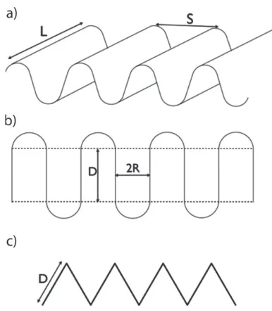
Fig. 2: Schematic diagrams of the corrugated geometry adopted by our graphene sheets. (a) Characteristic shape of corrugated sheets of graphene of width L with a periodicity S. For practical purposes we assumeL → ∞. (b) Cross sec-tion of the corrugated graphene sheet used in our calculasec-tions, whereby sections of curved graphene with curvature radiusR and widthπRare spaced by flat regions of width D. For dis-tinction, these two different regions are separated by the hor-izontal dashed lines. (c) In the limit R → 0, the corrugated sheet becomes a series of equally spaced sharp creases sepa-rated by flat sections of graphene.
either γ or λalone is not capable to induce the bandgap opening, as shown in figs. 1(b) and (c). Only when both quantities are non-zero, will the bandgap appear. This is explained by the fact thatγ andλ define two comple-mentary energy scales and the magnitude of the bandgap Δ is determined ultimately by the smallest of these two quantities.
Let us now consider folding the graphene sheet as a SOI-enhancing mechanism. In this case, however, the SOI is not homogeneously distributed but spatially limited to the region of the graphene sheet surrounding the non-planar deformations. We consider a corrugated structure where curved deformations to the graphene sheet are ordered in a periodic structure. This can be achieved by patterning a substrate in the form of periodic trenches [25,26] on top of which a graphene sheet is deposited. In this way, the graphene sheet alternates between curved and flat regions, the dimensions of which will depend on the geometry of the patterned substrate. Figure 2(a) shows an image of a typical corrugated sheet composed of a sequence of paral-lel ridges and troughs. While the diagram depicts a sheet of width L, it is supposed to represent a system where
to an array of half nanotubes joined seamlessly together by flat nanoribbons. Since the material has to comply dur-ing folddur-ing, this kind of distortion of the graphene sheet does not introduce the disorder that is so deleterious to the transport properties in other gap-opening proposals.
Differently from the previous case where we looked at how the electronic band structure changes with the in-clusion of the SOI plus the Zeeman term across the entire system, in the corrugated case we investigate how the con-ductance of the material responds to the addition of ex-actly the same ingredients, now in a periodic arrangement as shown in fig. 2(b). In this case both these ingredi-ents are added to the pristine Hamiltonian only where the graphene sheet has a non-zero curvature. The advantage of studying the transport response of the system is that we are able not only to identify the opening of a bandgap, which appears as a region of zero conductance, but we can simultaneously investigate the spin dependence of the transport response when the conductance is finite. In this way, we can study the appearance of a bandgap and as-sess its potential impact on spintronics applications at the same time.
Rather than using the Dirac equation to describe the electronic structure of the system, we consider the tight-binding (TB) Hamiltonian whose accuracy is not limited to a narrow energy range surrounding the Dirac point [27]. The Hamiltonian is written as ˆH =(ˆa†j,σˆbj,σ+h.c.)+ ˆV,
where the operators ˆa†j,σ (ˆaj,σ) creates (anihilates) an elec-tron at site j and spin σ on the sublattice A. The ˆb†j,σ
and ˆbj,σare the corresponding operators for theB sublat-tice. The operator ˆV =iλll
αβzˆ·(σαβ×dll)c†lαclβ− γlααc†lαclαrepresents the effects of a Rashba spin-orbit coupling [24] plus a Zeeman field. dll is the position of
sitelrelative to sitel. σis the vector formed by the Pauli matrices and the indexαin the last sum takes the value +1 for majority spins and −1 for minority spins. The Rashba term arises whenever inversion symmetry in the direction perpendicular to the graphene sheet is broken, a condition realized for samples deposited on a substrate or in the presence of an electric field perpendicular to the sheet plane.
The parametersλandγare dependent on the curvature and on the applied magnetic field, respectively. The for-mer can be estimated from refs. [14,15], which studied the SOI in carbon nanotubes, and the latter can be extracted from characteristic values of magnetic fields. For the case shown in fig. 2(b) the potential ˆV acts only where the curved regions are located. In other words, we must con-sider a graphene sheet with an array ofM equally spaced regions of width πR separated by a distanceD. Follow-ing refs. [14,15],λ is inversely proportional to the radius
R, which means that higher curvatures correspond to nar-rower curved sections with correspondingly stronger values
giving rise to a geometry depicted by fig. 2(c). In all cases, we assume that the corrugated structure is connected by leads made of semi-infinite pristine graphene.
The conductance is calculated by the Kubo formula ex-pressed in terms of the single particle Green function G, which in turn, is defined as G(E) = (Eˆ1−Hˆ)−1, where
E is the energy and ˆ1 is the identity operator. The zero bias DC conductance Γ is written as
Γ = 4e
2
h ReTr
[ ˜G]00t01[ ˜G]11t10−t01[ ˜G]10t01[ ˜G]10
. (3)
Here, ˜Glα,lβ = [Glα,lβ −(Glβ,lα)∗]/2i and [G]AB is the
matrix formed by the Green function elements connecting unit cellsA andB. αand β are spin indices. We define unit cells as lines along the “armchair” direction. The trace is taken over both site and spin indices. All Green functions above are evaluated at the Fermi level.
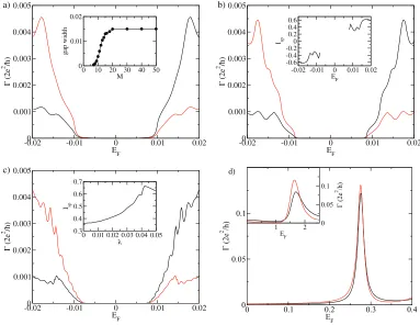
In fig. 3 we show the results for the spin-dependent conductance as a function of the Fermi level EF for M = 10, 15, and 50. Note the opening of a gap as M
increases, as shown in the inset of fig. 3(a). The mag-nitude of the gap increases with M but saturates when
M 1. In addition, outside the gapped energy region, the conductance becomes spin dependent,i.e., the trans-port properties for the ↑ and ↓ spin electrons become asymetric, which is a basic requirement for exploring the use of any material in spintronics. Such an asymmetry in the spin-dependent conductance means that these cor-rugated systems can function as spin polarizers for the electronic currents in graphene. The inset of fig. 3(b) shows the spin-polarization of the current, defined as
Isp = (I↑ −I↓)/(I↑+I↓), as a function of EF whereas the inset of fig. 3(c) depicts Isp as a function of λ. Note the sign change ofIspon either side of the bandgap. This feature is seen in all our results.
To assess the robustness and generality of these findings we make use of a simplified approach that is less compu-tationally involved and yet capable of capturing the con-tribution from the two key ingredients, namely the SOI and the Zeeman term. We investigate the limit R → 0, shown schematically in fig. 2(c). In this limit, the SOI-enhancing curvature becomes extremely large at the same time as the extension of the curved region becomes vanish-ingly small. The smooth ondulations shown in figs. 2(a) and (b) give way to equally spaced creases on the graphene sheet, ideally represented by Dirac delta functions that mark the locations where both the SOI and the Zeeman term are non-zero. Moreover, a further simplification is to assume electrons moving along the direction normal to the creases. The Hamiltonian in this case becomes
ˆ
H = ˆH0+Mj=1V δˆ (x−jD), where the operators ˆH0and ˆ
A. T. Costaet al.
-0.02 -0.01 0 0.01 0.02
EF 0 0.001 0.002 0.003 0.004 0.005 (2e 2 /h)
0 10 20 30 40 50 M 0 0.01 0.02 gap width a)
-0.02 -0.01 0 0.01 0.02
EF 0 0.001 0.002 0.003 0.004 0.005 (2e 2 /h)
-0.02 -0.01 0 0.01 0.02 EF -0.6 -0.4 -0.20 0.2 0.40.6 Isp b)
-0.02 -0.01 0 0.01 0.02
EF 0 0.001 0.002 0.003 0.004 0.005 (2e
2 /h) 0.30 0.01 0.02 0.03 0.04 0.05 0.4 0.5 0.6 0.7 Isp c) 1 2 EF 0 0.05 0.1 Γ (2e 2 /h)
0 0.1 0.2 0.3 0.4
EF 0 0.05 0.1 Γ (2e 2 /h) d)
Fig. 3: (Colour on-line) Spin-dependent conductances of a corrugated sheet made ofM curved regions of radius R ∼ 6 ˚A separated by flat sections of graphene of widthD= 20. Except for the insets, black (red) lines represent↑ (↓) spin-polarized conductances. (a)M= 10;γ= 5×10⁻²;λ= 5×10⁻². The inset shows how the conductance gap scales withM. Note that it tends to a saturation value whenM 1. (b)M = 15;γ= 5×10⁻²;λ= 5×10⁻². The inset depicts the spin polarization of the currentIspas a function ofEF. Only results outside the bandgap are shown. (c)M = 50;γ= 5×10⁻²;λ= 5×10⁻². Shown in the inset is the dependence ofIspon the SOI parameterλ. (d) Results for creased graphene sheets represented schematically by fig. 2(c) forM= 2 delta functions for electrons constrained to move perpendicularly to the creases calculated based on the TB-model (main figure) and on the simplified model (inset).
massless particles under the action of a perturbing poten-tial made of a series ofλ- andγ-dependent delta functions. It is worth mentioning that the boundary conditions used to solve the Dirac equation in the presence of delta func-tion potentials are not the same as those commonly used to solve the Schroedinger equation. The wave function for Dirac electrons is not continuous around a delta function but obeys the following condition [28]: ψ+=eAψ−, where
ψ+ andψ− are the wave function for the Dirac electrons to the right and left of the delta function, respectively. In the case considered here, the operatorAis given by
A=−
⎛ ⎜ ⎜ ⎜ ⎝
0 0 −i 0 0 0 0 −i
i 0 0 0
0 i 0 0 ⎞ ⎟ ⎟ ⎟ ⎠
−1⎛
⎜ ⎜ ⎜ ⎝
−γ 0 0 −2iλ
0 γ 0 0
0 0 −γ 0 2iλ 0 0 γ
⎞ ⎟ ⎟ ⎟ ⎠. (4)
It is then straightforward to calculate the transmission co-efficient of electrons across this potential and plot it as a function of the energy, which is proportional to the wave vectork. Since the conductance is also proportional to the transmission coefficient, we can now compare the results
of this simplified approach with the TB-based results. In fig. 3(d) we show results forM = 2 delta functions calcu-lated with the simplified approach as well as with the TB adapted for normal incidence. Quantitative agreement is not expected because the discrete delta function represen-tation in the TB-model is fundamentally different from the continuous one. From a qualitative point of view, however, both methodologies lead to the appearance of a low-energy conductance gap followed by a spin-polarized current for energies outside the bandgap. This commonal-ity found with two distinct methodologies is indicative of the robustness of our findings, which is further confirmed by recent calculations based on Density Functional The-ory results also displaying bandgap features when the SOI is enhanced by curvature effects [29].
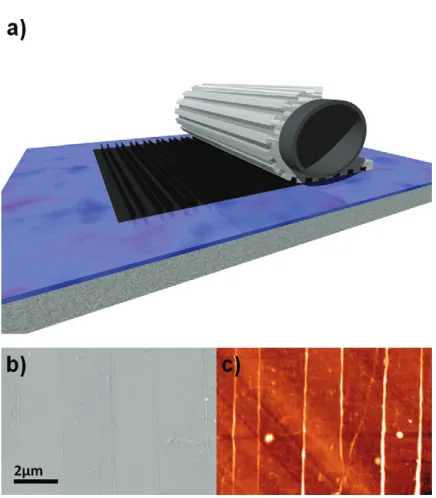
[image:5.595.102.485.85.381.2]Fig. 4: (Colour on-line) Experimental method used to grow fin-like structures made of a single folded graphene sheet. (a) A graphene sheet draped over a relief patterned PDMS stamp is used to print free standing graphene fins in a mod-ified transfer printing technique. (b) A scanning electron mi-crograph and (c) an AFM image of a small portion of a folded graphene surface.
splitting may induce a spin splitting within the underly-ing carbon atoms via hybridisation. The induced split-ting will be equivalent to a large Zeeman field. While we are not able to quantify the precise contributions coming from each one of the different mechanisms, curvature and dopants acting jointly together will certainly amplify the overall effect of spin-polarization of the charge currents as well as the bandgap in the electronic structure of the system.
Regarding the experimental feasibility of the sys-tem considered in this theoretical study, the syssys-tem schematically depicted by fig. 2(a) is easily realized if graphene sheets are deposited on periodically trenched substrates [26]. Despite being experimentally more chal-lenging, the creased structures shown in fig. 2(c) are also possible and are currently grown with impressive levels of control on their dimensions and periodicity as illustrated in fig. 4. The graphene is transferred via a PMMA sup-port layer onto a trenched PDMS stamp with a conven-tional polymer assisted process [30]. The PMMA is then removed with a solvent bath and with controlled drying conditions the graphene film sinks into the trenches on the stamp. Upon further drying of the graphene, it partly ad-heres to the trench walls with a suspended configuration over the middle of the trench. Printing the graphene inked stamps leads to the suspended graphene collapsing onto the substrate and the adhered side-wall graphene folding into a bi-layer configuration as shown in fig. 4(a). As a
AFM image of a small portion of such a printed surface is depicted in fig. 4(c). It is worth emphasizing that this methodology gives us full control on the dimensions and periodicity of the folded fins. The remaining challenge consists of carrying out transport measurements across such structures but the fact that they are grown with such an excellent level of control is the first step towards the experimental confirmation of our theoretical predictions.
In summary, we have shown that by adding the Zee-man term and the SOI to the Hamiltonian of pristine graphene, we force the opening of a bandgap in its elec-tronic structure and induce its charge current to become spin-polarized. Both additions to the Hamiltonian are experimentally feasible and are mimicked by an externally applied magnetic field and by deforming the graphene sheet out of its planar geometry through folding. It is worth mentioning that our findings are valid not only for the type of 1-dimensional folding here suggested but should arise whenever strain-enhanced spin-orbit interac-tion coexists with any spin-splitting mechanism. With the increasing degree of experimental control on both the chemistry and the geometry of nanoscaled surfaces, it is possible that by engineering the shape and composition of graphene sheets we can create spin-polarized currents in an energy-gapped material. Such an origami-like tech-nique is likely to bring about a whole new range of spin-tronic features in 2-dimensional systems not possible in 3-dimensional structures.
∗ ∗ ∗
MSF acknowledges financial support from Sci-ence Foundation Ireland under Grant Number SFI 11/RFP.1/MTR/3083. AHCN acknowledges DOE grant DE-FG02-08ER46512, ONR grant MURI N00014-09-1-1063, and the NRF-CRP award “Novel 2D materials with tailored properties: beyond graphene” (R-144-000-295-281). ATC acknowledges partial financial support from CNPq (Brazil) and INCT Nanomateriais de Car-bono. GSD acknowledges support from SFI under grant PI-10/IN.1/I3030.
REFERENCES
[1] Geim A. K.andNovoselov K. S.,Nat. Mater.,6(2007) 183.
[2] Novoselov K. S., Falko V. I., Colombo L., Gellert P. R., Schwab M. G.andKim K.,Nature, 490(2012) 192.
[3] Han M.et al.,Phys. Rev. Lett.,98(2007) 206805. [4] Cai J. M.et al.,Nature,466(2010) 470.
[5] Ohta T.et al.,Science,313(2006) 951.
[6] Oostinga J. B.et al.,Nat. Mater.,7(2008) 151. [7] Klinovaja J., Ferreira G. J.andLoss D.,Phys. Rev.
B,86(2012) 235416.
[image:6.595.56.274.76.325.2]A. T. Costaet al.
[9] Ni Z. H., Yu T., Lu Y. H., Wang Y. Y., Feng Y. P. andShen Z. X.,ACS Nano,2(2008) 2301.
[10] Mohiuddin T. M. G., Lombardo A., Nair R. R., Bonetti A., Savini G., Jalil R., Bonini N., Basko
D. M., Galiotis C., Marzari N., Novoselov K. S.,
Geim A. K.andFerrari A. C.,Phys. Rev. B,79(2009) 205433.
[11] Peres N. M. R.,Rev. Mod. Phys.,82(2010) 2673. [12] Elias D. C.et al.,Science,323(2009) 610. [13] Loh K. P. et al.,J. Mater. Chem.,20(2010) 2277. [14] Huertas-Hernando D., Guinea F. and Brataas A.,
Phys. Rev. B,74(2006) 155426.
[15] Huertas-Hernando D., Guinea F. and Brataas A.,
Phys. Rev. Lett.,103(2009) 146801.
[16] Guimaraes F. S. M., Kirwan D. F., Costa A. T., Muniz R. B., Mills D. L.and Ferreira M. S.,Phys.
Rev. B,81(2010) 153408.
[17] Guimaraes F. S. M., Costa A. T., Muniz R. B.and Ferreira M. S.,Phys. Rev. B,81(2010) 233402. [18] Tombros N., Jozsa C., Popinciuc M., Jonkman H. T.
andvan Wees B. J.,Nature,448(2007) 571.
[19] Pesin D.andMacDonald A. H.,Nat. Mater.,11(2012) 409 and references therein.
[20] Han W., Chen J., Wang D., McCreary K. M., Wen H., Swartz A. G., Shi J. andKawakami R. K.,Nano
Lett.,12(2012) 3443;McCreary K. M., Swartz A. G., Han W., Fabian J.and Kawakami R. K., Phys. Rev.
Lett.,109(2012) 186604.
[21] Balakrishnan J., Koon G. K. W., Jaiswal M.,
Castro Neto A. H. and Ozyilmaz Barbaros¨ , Nat.
Phys.,9(2013) 284.
[22] Castro Neto A. H.and Guinea F., Phys. Rev. Lett.,
103(2009) 026804.
[23] Ma D., Li Z.andYang Z.,Carbon,50(2012) 297. [24] Kane C. L.andMele E. J.,Phys. Rev. Lett,95(2005)
226801.
[25] Hicks J.et al.,Nat. Phys.,9(2013) 49.
[26] Winters S., Hallam T., Nolan H. and Duesberg G. S.,Phys. Status Solidi B,249(2012) 2515.
[27] Power S. R. and Ferreira M. S., Phys. Rev. B, 83 (2011) 155432.
[28] Gomes J. V.and Peres N. M. R.,J. Phys.: Condens.
Matter,20(2008) 325221.
[29] Avdoshenko S. M., Koskinen P., Sevincli H., Popov A. and Rocha C. G., Sci. Rep., 3 (2013) 1632, arXiv:1301.2226.
[30] Li X.et al.,Science,324(2009) 1312.