880
©IJRASET: All Rights are Reserved
Design of Low Power Full Adder Using ONOFIC
Approach
Ashly Thomas 1, Sheela Devi Aswathy Chandran2
1
PG Scholar, Dept. of ECE, TKM Institute of Technology, Kollam, Kerala, India. 2
Asst. Professor, Dept. of ECE, TKM Institute of Technology, Kollam, Kerala, India.
Abstract: Improving performance with reduced power consumption and chip area are the main constraint for designing VLSI CMOS circuits. The high performance low power ONOFIC approach for VLSI CMOS circuits reduces the power dissipation and improves the speed of a VLSI circuit design. In this paper, high performance and low power full adder based on ONOFIC approach have been implemented. The proposed method reduces the power dissipation and improves the speed of full adder circuit . The On/Off logic (ONOFIC) approach reduces the leakage current and leakage power with simple and single threshold voltage circuit level approach. This approach efficiently reduces the leakage current in both active and standby mode of logic circuit. The tool used for implementing the design is EDA TANNER 13.0 tool. The ONOFIC approach results have been compared with LECTOR technique and observed that the ONOFIC approach shows the improved performance and reduced power dissipation.
Keywords: Leakage Current, ONOFIC, LECTOR, EDA TANNER 13.0.
I. INTRODUCTION
Power dissipation is a key consideration in the design of nano-scale CMOS VLSI circuits. The main sources of power dissipation are: 1) Dynamic power dissipation due to the charging and discharging of the load capacitance. 2) Short-circuit current due to the existence of a conducting path between the voltage supply and ground for the brief period during which a logic gate makes a transition. 3) Leakage current. The leakage current consists of reverse-bias diode currents and sub threshold current. The former is due to the stored charge between the drain and bulk of active transistors while the latter is due to the carrier diffusion between the source and drain of the OFF transistors. Also, gate induced drain leakage and gate direct tunneling leakage have become the significant sources of leakage power. In deep submicron CMOS technologies, the role of sub threshold leakage power dissipation becomes dominant among other leakage power components.
Modern portable electronic devices such as mobile phones, laptops, PDA’s (personal digital assistant) etc are affected by high power consumption which reduces the battery backup time. The device density of these devices has been increased to improve the performance of the circuit. So there is a need for low power design methodology to limit the power consumption in high density VLSI chips. Voltage scaling is one of the effective techniques to reduce the power consumption in electronic devices. In electronic devices, to control the power consumption a supply voltage plays an important role. Supply voltage scaling without scaling of threshold voltage degrades the performance of the device. By reduction of threshold voltage and supply voltages proportionally retains the performance. The threshold voltage reduction leads to the five times higher leakage current. Adopting new lower level technologies leads to the increase in power dissipation in integrated circuits. A perfect designer concentrates mostly for efficient techniques for leakage current reduction in deep sub micron regime. For high performance and low power CMOS circuits On/Off logic (ONOFIC) approach can be implemented in VLSI circuits. It reduces the power dissipation and improves the speed of a VLSI circuit design. The ONOFIC approach efficiently reduces the leakage current in both active and stand by mode of logic circuit. It introduced the extra logic between pull-up and pull-down networks for leakage reduction. This additional introduced logic circuit is known as On/Off logic (ONOFIC) circuit. The ONOFIC logic circuit contains one PMOS and one NMOS transistor. Due to maintaining on or off condition for any output logic level this circuit is called as ONOFIC. In this paper to design a low power full adder, the ONOFIC approach is implemented in it and then compared with LECTOR logic. The results show that the propagation delay and power dissipation is low for ONOFIC when compared with LECTOR.
II. LITERATUREREVIEW
881
©IJRASET: All Rights are Reserved
transistor) having the same threshold voltage as that of nMOS transistors of the logic circuit is inserted between the logic circuit and ground.
LECTOR technique utilizes two leakage control transistors (LCT) which are inserted between PUN (Pull Up Network) and PDN (Pull Down Network) circuit within the logic gate for which the gate terminal of each leakage control transistor is controlled by source of other[4] .This arrangement ensures that one of the leakage control transistor always operate near it’s cut off region. Leakage control transistors causes increase in the resistance of the path from Vdd to ground, since one of the LCT’s always near its cut-OFF region, therefore decreasing the leakage current[7]. The basic idea behind LECTOR approach is that a state with more than one transistor OFF in a path from supply voltage to ground is far less leaky than a state with only one transistor OFF in any supply to ground path[6]. In case of near cut off operation of transistors the resistance of the transistor is high as an OFF transistor’s resistance but the available resistance is sufficient to increase the supply voltage to ground path resistance and so to reduce the leakage power dissipation. This technique is good for leakage reduction but this technique is not capable of reducing propagation delay.
III.ONOFICAPPROACH
The On/Off logic (ONOFIC) approach reduces the leakage current and leakage power with simple and single threshold voltage circuit level approach. This approach efficiently reduces the leakage current in both active and standby mode of logic circuit. It introduces an extra logic between pull-up and pull-down networks for leakage reduction as shown in Fig.1. This additional introduced logic circuit is called as On/Off logic (ONOFIC) circuit. The ONOFIC logic circuit contains one PMOS and one NMOS transistor. The connection of ONOFIC transistors is as shown in Fig. 2.
882
©IJRASET: All Rights are Reserved
Fig.2 .Connection of ONOFIC transistors.
Due to maintaining on or off condition for any output logic level this circuit is called as ONOFIC. This logic directly affects the power dissipation and propagation delay of the logic circuit. ONOFIC circuit uses the logic of force stacking for controlling the leakage current by providing the maximum resistance to the ONOFIC block when it is in off state and minimum resistance when it is in on state. In ONOFIC block the operation of NMOS transistor is controlled by a PMOS transistor. Depending on the output logic ONOFIC NMOS or PMOS transistors must be in cut-off or in linear mode.
In ONOFIC block, the drain of PMOS transistor is connected to the gate of NMOS transistor and the output is connected to the gate of PMOS transistor. The drain of the pull down network is connected to the source of NMOS transistor and PMOS source terminal is connected to VDD of the circuit. The NMOS transistor drain is connected to the output of the circuit and the substrate of NMOS transistor is connected to the ground while the substrate of PMOS transistor is connected to the VDD. The main concept of this technique is the property of on/off. The both ONOFIC transistors are in linear region when ONOFIC logic is in on condition while both transistors are in cut-off mode if ONOFIC logic is in off state. This reduces the leakage current at both active and standby mode with accurate logic level at the output. The good conducting path is obtained by turning on the ONOFIC block and it acts as a good resistance to control the leakage current when it is in off state.
IV.IMPLEMENTATIONCIRCUITANDMETHODOLOGY
The addition is a basic arithmetic operation and act as the core of other arithmetic operations like multiplication, division, subtraction, address generation etc. Adders are the key element in many VLSI systems such as microprocessors, ALU’s, multiplexers, comparators, parity checkers, digital signal processing (DSP) architectures, code converters etc. The most required feature of modern electronics is low power energy efficient building block that enables the implementation of long lasting battery operated systems. Full adders are the fundamental circuit elements of VLSI systems. For performance analysis of various full adders different parameters are measured like power dissipation, delay, number of transistors used and power delay product of circuit. In a low power design it is optimized and desired that the circuit consume less power, have very less delay, low supply voltage and avoid degradation in output voltage . There is no ideal full adder circuit which can be single handily used in all types of applications. It is very important for circuit design to have good drivability under different load conditions and also balanced output to avoid glitches. The time delay depends on size of transistors, number of transistors used, logic depth, parasitic capacitance and capacitance due to intercell and intracell routing and also on number of inversion levels . A full-adder is a logic circuit having three inputs A,B and C ( which is the carry from the previous stage) and two outputs (Sum and Carry). The full-adder can handle three binary digits at a time and can therefore be used to add binary numbers in general. The simplest way to construct a full adder is to connect two half- adder and an OR gate.
883
©IJRASET: All Rights are Reserved
Fig.3. Circuit diagram of full adder.
V. RESULTS
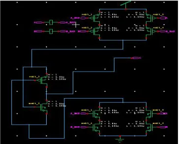
Fig.4 shows the circuit diagram of full adder using two half adder . Each half adder module consist of an XOR and AND gate. The input bits A and B are applied to an XOR gate and an AND gate respectively. The output obtained from the XOR gate and the input bit C is given to the XOR gate and the AND gate in the second half adder module . The output thus obtained from the XOR gate in the second half adder module is the sum. The output of the AND gates from both the module is then given to an OR gate and obtained the carry. Figure 5 shows the implementation of the circuit using EDA TANNER tool.
Fig.4. Implementation of Full adder Circuit
884
©IJRASET: All Rights are Reserved
Fig 5.1(a) XOR Gate Using ONOFIC logic Fig 5.1(b) XOR Gate Using LECTOR logic
The simulation results shows the propagation delay and the power dissipation obtained while implementing the ONOFIC (Fig. 5.2 (a) and Fig.5.2(c) ) and the LECTOR logic (Fig.5.2 (b) and Fig.5.2(d) ).
Fig.5.2 (a) Propagation delay in ONOFIC Fig.5.2 (b) Propagation delay in LECTOR
[image:5.612.80.266.78.227.2]
Fig.5.2 (c) Power dissipation in ONOFIC Fig.5.2 (d) Power dissipation in LECTOR
Table.1 Comparison Between Onofic And Lector Parameter
Logic
Power Dissipation Propogation Delay
ONOFIC 2.295e-007W 1.68 seconds
LECTOR 3.8125e-006W 2.17 seconds
From the Table 1 it is observed that the power dissipation and propogation delay obtained in ONOFIC approach is lower when compared to the LECTOR technique, The simulation results gave the propogation delay and the power dissipation obtained while implementing the ONOFIC and the LECTOR logic . Comparison between ONOFIC and LECTOR is shown in the Table 1.
VI.CONCLUSIONS
[image:5.612.349.532.80.226.2] [image:5.612.127.461.498.615.2]885
©IJRASET: All Rights are Reserved
[1] Umesh Jeevalu Chavan, Siddarama R Patil “High Performance and Low Power ONOFIC Approach for VLSI CMOS Circuits Design”.IEEE Conference on Communication , April 2016.
[2] Partha Bhatatacharyya,“ Performance Analysis Of A Low Power High Speed Hybrid 1- Bit Full Adder Circuit”.10.11.09\TVLSI’ 2014’2357057 IEEE ,23 pp. 1036–8210.
[3] Rohit Lorenzo, And Saurabh Chaudhury “A New Low Leakage And High Speed Technique For CMOS Circuits”. IEEE 2014 978-1-pp. 4799- 4939-7/14. [4] HeungJun Jeon , Yong Bin Kim “Standby Leakage Power Reduction Technique For Nanoscale CMOS VLSI Systems ” IEEE 2010.
[5] Surabhi Sing, Baljit Kaur And S. Dasguota. Leakage Current Reduction Using Modified Gate Replacement Technique For CMOS VLSI Circuits”.IEEE 2012. [6] Hanchate And N. Ranganathan, “A Technique For Leakage Reduction In CMOS Circuits IEEE Transaction On Very Large Scale Integration(VLSI
Systems),12,196-205
[7] K.C Tung Y.C Hung Shieh And S.G Hung “A Low Power High Speed Hybrid CMOS Full Adder For Embedded System ”In Proce IEEE Conf, Design Diagnostic Electron Circuits Syst Vol -13 Apr-2007 pp14.
[8] T. Hiramoto and M. Takamiya: “Low Power and Low Voltage MOSFETs with Variable Threshold Voltage Controlled by Back-Bias”, IEICE Trans. Electron., vol. E83-C, pp. 161-169, 2000
[9] Radhakrishan D. “Low Voltage Low Power CMOS Full Adder ”IEEE Proc-Circuits Vol148 No 1 Pp 19-24 2001
[10] Armin Tajalli “Leakage Current Reduction Using Subthresold Source- Coupled Logic” Presented Microelectronics System Laboratory ,Swiss Fedral Institute Ch-1015 Lausanne, Switzerland 2008.
[11] Morteza Rohimian, Alli A Aminbeidokhti Amirhossein”31nm High Current Performance Double Gate Mosfet For Low Power CMOS Circuits” Pubblished In Toyoi And Francies 37-41 Mactime Street London WIT 3JH UK.