Study of Two One-Dimensional Multi Tunnel Junctions
Arrays Structures by SIMON
Amine Touati, Samir Chatbouri, Nabil Sghaier, Adel Kalboussi
Laboratory of Microelectronics and Instrumentation, Faculty of Sciences of Monastir, University of Monastir, Monastir, Tunisia Email: [email protected]
Received August 18, 2012; revised September 20, 2012; accepted October 4,2012
ABSTRACT
Multi Tunnel Junctions (MTJs) have attracted much attention recently in the fields of Single-Electron Transistor (SET) and Single-Electron Memory (SEM). In this paper, we investigate a nano-device structure using a two one dimensional array MTJs connected to the basic Single Electron Circuits, in order to analyze the impact of physical parameters on the performances and application of this structure. The device generates can operate at room temperature. The simulation of single-electron circuit demonstrates with Monte Carlo simulator, SIMON.
Keywords: Multi Tunnel Junctions (MTJs); Coulomb Blockade Effect; Effective Capacitances; SIMON Simulator
1. Introduction
As the semiconductor device feature size enters the sub- 50-nm range, two new effects come into play. One is the quantum effect, which is rooted in the wave nature of the charge carriers, and gives rise to non classical transport effects such as resonant tunneling and quantum interfer-ence. The other is related to the quantized nature of the electronic charge, often manifested in the so-called sin-gle-electron effect: Charging each electron to a small confined region requires a certain amount of energy in order to overcome the Coulomb repulsion; if this charg-ing energy is greater than the thermal energy, kBT (kB:
Boltzmann constant, T: temperature), a single electron added to the region could have a significant effect on other electrons entering the confined region.
Single-Electron Transistors (SETs) operate using a Coulomb blockade, which occurs in tiny structures made of conductive material due to electrostatic interactions between confined electrons. There are basically two types of SET application: memory devices [1] and logic func-tions have been proposed [2]. The small size is especially important for memory devices; memory cells have to be small to achieve a greater degree of integration.
Since the very early demonstration of the single-elec- tron charging effect [3] a number of advances has been made. Low temperature experiments on the single-elec- tron turnstile [4] have established and proven their work- ing principle. Single-electron devices have also been applied to metrology, where a Coulomb blockade ther- mometry has been proposed [5].
For the future ultimate application of SETs, we must
first succeed in the manipulation and the detection of a single electron. Basic demonstrations of single-electron transfer devices have been achieved at low temperatures, and some have even been realized at room temperature [6,7].
Raising the operating temperature as high as room temperature means that we have to reduce the island size of the order of a few nanometers. Although this is a challenging issue, some devices have been demonstrated that clearly and conclusively operate at room temperature through the use of recent rapidly developing nanotech- nologies. The results provide excellent prospects for the future practical application of SETs.
The Multiple-Tunnel Junction (MTJ) consists of a one chain of nanoscale islands and tunnel junctions. In such a system, the single-electron charging of each island, and the effect of excess electrons on the polarization of neighboring tunnel junctions, modifies the Coulomb blockade region, and the I-V characteristics of the system. Furthermore, the single-electron charging energy of an island embedded within a chain of islands and tunnel barriers is also increased somewhat. The effective total capacitance of the system can be decreased and hence the charging energy EC and operating temperature Tmax in-creased within the same fabrication technology by re-placing the single junction of the transistor with short one-dimensional (1D) arrays. This raises the maximum temperature where single-electron effects are observed, in comparison with a simple double tunnel junction of similar island capacitance.
2. Theory
[image:2.595.64.284.568.686.2]2.1. Cell Design and Description
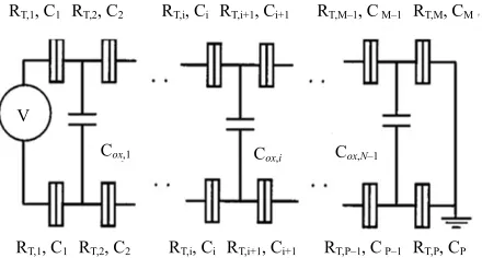
Figure 1 shows the circuit diagram for a two 1D MTJ with (M − 1) islands, and M tunnel junctions in first line, and (P − 1) islands, and P tunnel junctions on the second line. The islands are separated from each other and from the source and drain regions at the ends, by tunnel junc-tions with capacitance C. The remaining capacitance of each island is represented by C, and a bias V is used to inject electrons into the MTJ. The source is connected to the ground. Thus will reduce the error to the order 1/MP, where M and P are the number of junctions in parallel and in series respectively. For numerical calculations, we used our universal single-electronics simulation program SIMON [8,9] based on a Monte Carlo approach.
The oxide layer separating the two MTJs is shown in Figure 1 by a capacitor Cox. Such as approximate ex- pression of the capacity of oxide:
0
d r ox
S
C (1)
The dynamics of the system are governed by the fol-lowing equation which gives the tunneling rate of an electron in each one of tunnel junctions by using the “or-thodox theory” [10] of single electron tunnelling:
1
² 1 exp ij i j
T ij B
F
e R F k T
(2)
whereΔFij = ΔFi – ΔFj = –eVds is the difference between the free energy of the initial and final states, where Vds is the source voltage, and RT is the tunneling resistance of the junction. The tunneling rate of global system it is:
1 2 ' '
i j i j
M P
(3)where Γ1,2 denote the first and second arrays respectively.
The sum is made on the M and P MTJs. The theory of uniform one 1D arrays of tunnel junctions is well devel-
RT,1, C1 RT,2, C2 RT,i, Ci RT,i+1, Ci+1 RT,P–1, C P–1 RT,P, CP RT,1, C1 RT,2, C2 RT,i, Ci RT,i+1, Ci+1 RT,M–1, C M–1 RT,M, CM
V
Cox,1 Cox,i Cox,N–1
Figure 1. A circuit diagram of tow one-dimensional array of tunnel junctions. Junction i is characterized by its tunnel resistance RT,iand capacitance Ci in parallel and islands have a oxide capacitance Cox,i .
oped for the case of low temperatures, kBT << Ech = e²/CΣ
[11,12]. When the temperature becomes so high that the energy scale of thermal fluctuations kBT exceeds of the single-electron addition energy Ec, these fluctuations smear the Coulomb blockade, making the operation of the transistor impossible. The Monte Carlo simulations show that the tunnel junction capacitance C which is used in the equations for one 1D array should be replaced in the two 1D case by an effective capacitance Ceff which is higher than the real capacitance.
Experimentally, MTJs with constant values of C and
Cox have been fabricated mainly using metal islands [13]. An important property of the two 1D array is that it can be fabricated with lower resistance than a one 1D array, even if it contains many junctions in series. For a good functioning of the structure and to avoid degradation of the system we must choose a high number of junctions
The charging energy of the island creates an energy barrier which blocks the entrance of electrons into the MTJ so that multistable states of different numbers of electrons can be formed. The MTJ is also important in suppressing co-tunneling effects; that is, electron tunnel-ing simultaneously across more than one junction.
2.2. Physicals Parameters
The tunneling occurs through one tunnel junction and the simultaneous tunneling of electrons across the other junctions is neglected. When the tunneling through 2M
(M = P) junctions is considered, the other junctions be-have simply as capacitors. The effective capacitance Ceff at island is given by:
eff i ox
C C C (4)
where
2
2 1
i
M C
M C
(5)
In an infinite 1-D array, the capacitance between two neighboring islands is exactly twice the capacitance of the tunnel junctions, and this is the reason that the offset voltage is a factor of 2 lower in a two 1-D array com-pared to a one 1D array.
For the kth island, the potential is given by:
k eff
e V
C
(6)
This may be used to write the potential at the (k –1)th island.
The effective charging energy, Ec,MTJ is defined
simi-larly to the usual charging energy, except the physical capacitance is replaced with the effective capacitance:
2 ,
2 ch eff
eff
e E
C
Applying a large enough voltage V will inject a elec-tron into the MTJ, and a current begins to flow. The threshold voltage when this occurs is given by:
th eff
e V
C
(8)
The value of the threshold voltage is low compared to the voltage corresponding to the sum of the individual charging energies of the islands. This is because the ap-plied voltage drops more across the first junction, closest to the voltage source, due to the presence of the stray capacitance Cox at the first island. We have further-more assumed that the offset voltage of a two one dimensional arrays of tunnel junctions is:
off
V = 4
Ne
C (9)
3. Simulation Results
3.1. I-V Characteristic
We will now consider the I-V characteristics of the two 1-D MTJs. As the bias V increases, the number of transi- tions in the MTJs increases (Figure 2(b)). We consider a simple two island MTJ, where the electron numbers on the islands are n1 and n2 respectively. The charge state of
the MTJ without any extra electrons may be expressed as (n1, n2) = (0, 0) [14]. When a bias V > Vth is applied, an
electron tunnels onto the first island, creating the state (1, 0). This electron can then move through the MTJ, through the states (0, 1) to (0, 0) as it leaves the MTJ. However, as the applied voltage is increased, other tran-sitions become possible, e.g. one may transition from the state (0, 1) either to the state (0, 0) or to the state (1, 1). These additional transitions lead to an increase in the current. For a longer MTJ, larger numbers of transitions are possible.
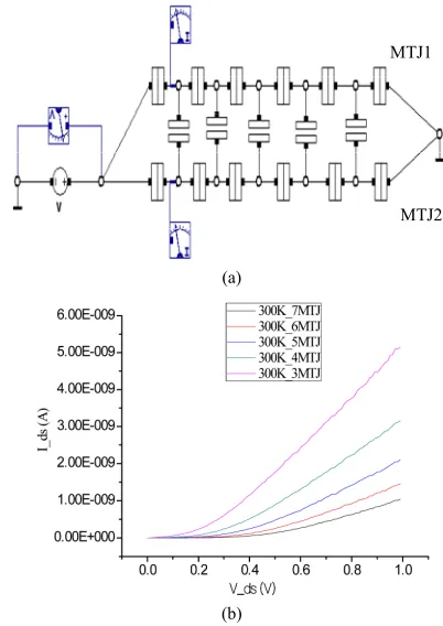
The theoretical results presented give that Ceff= 0.52 aF; Ceff is lower than the total capacitance attached to an island 2CT+ Cox= 0.8 aF; and Ech,eff= 0.15 eV = 6 kBT
(kBT = 0.025 eV at 300 K), this proves that the charging energy is much higher than the thermal energy. Therefore increase the number of tunnel junctions network can overcome the effect of low capacity and temperature operating. The staircase is typically irregular, with varia-tion in the step heights and widths. The blocking region is more important, also when the number of junctions increases for 2 × 7 MTJs. The threshold voltage is 0.3 V from (Equation (8)), and from the curve it is ~0.4 V. The current I it changes from ~1 nA (7 MTJs in parallel) to ~ 5.2 nA for 3 MTJs.
For the effects of bias voltage Vds, we find that it has a more effect on the electron tunneling than that of the one single electron tunneling, i.e. Single-Electron Transistor (SET), at some favored value more than of the Coulomb
blockade voltage.
Also, the tunneling rate of global system has a new factor so that: ' where α is factor which
de-pend on the effect of stray capacitor; with stray capaci-tances, the change of the Gibbs free energy due to the cotunneling process.
A typical result (Figure 3) has shown that the main effect of the stray capacitances is to reduce the threshold
MTJ1
MTJ2
(a)
[image:3.595.318.519.193.477.2](b)
Figure 2. A SIMON (a) equivalent circuit of a device with two 1-D MTJs consisting of 10 islands and 11 MTJs with C = 3 × 10–19 F,
Cox= 2 × 10–19 F and RT= 40MΩ. C, Cox, and RT represent the tunnel junctions capacitance, oxide ca-pacitance, and tunnel resistances, respectively; (b) Drain current vs. source-drain voltage characteristics at T = 300 K. 3, 4, 5, 6 and 7 MTJ denote the number of tunnel junctions in each array.
[image:3.595.331.513.580.709.2]temperature, and the I-V curve is not looks ohmic attitude. Also the increase in the temperature increase the conduc-tivity and this due to excited states of the array that are thermally populated, which contribute to the current. voltages, whereas it has very little effect on the
magni-tude of the tunneling current [15,16]. In general, when the stray capacitances increase, the I-V curve of the sin-gle-electron device is shifted towards the low-voltage side.
The clear Coulomb staircase suggests a strong asym-metry in the junctions along the MTJ, and this may be modeled by means of a random variation in the tunnel junction resistances RT, associated with the observed variation in nanocrystal separation.
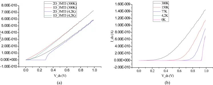
3.2. Temperature Effect on Device
Figure 4(a) show the behavior of I-V at 4.2 K and 300 K for one dimensional and two dimensional arrays respec-tively. At low temperature the curve exhibited no current in the range of applied voltage from 0 to 0.3 V for two 1-D arrays; the Coulomb blockade (CB) region but for one 1D we do not observe clearly the CB zone. However, at room temperature for one dimensional device showed a linear increase even in the zero bias regions, on the other hand, for two one dimensional structures we can perceiving the transistor performance. This means that electron tunneling was suppressed because the charging energy of the nanoparticle was sufficiently larger than the thermal fluctuation energy at 300 K.
3.3. Device Function with Two Gate Voltages For the applications of that structure, such as the multiple value logic (MVL) circuits [17], logic memory circuit [18] and hybrid SET-MOS [19], we need to have a gate or multi-gates allows more than two levels of logic. So we have added to the circuit in the Figure 2(a), two gates for each array; generally the two gates, one gate is used as voltage input port and the other gate is used as thresh- old voltage adjusting port. Single-electron current oscil- lations are observed in the Ids-Vgs characteristics Figure 5 without degradation like we have a simple SET, the os-cillations persist up to 300 K with an unchanged period. The oscillation periods increase when the temperature Then we have tried to see the effect of temperature on
the two 1-D device Figure 4(b), the CB zone is con-tracted when the temperature increase. The conduction current is activated at higher temperatures even at low
[image:4.595.113.486.377.526.2]
(a) (b)
Figure 4. Monte Carlo simulation of the Ids-Vds characteristics (a) of one and two 1D-MTJs at 4.2 K and 300 K; (b) Tempera-ture effect on two 1D with 7 MTJs in parallel.
[image:4.595.99.498.565.709.2]
(a) (b)
and drain-source voltage are increased, and decrease when the T and Vds are decreased.
The decrease in the oscillation period with increasing width implies an increase in the island capacitance. This is because the gate-islands capacitances (Cs) now are associated with the part of the electric field between the gates and island which passes through the oxide. The effect of the quantum dot size can be observed directly in the single-electron characteristics, as this is proportional to the island capacitance and therefore determines the Coulomb gap and the current oscillation period.
4. Conclusion
We have studied the temperature influence on one of promising single electron system that consists of two parallel 1D arrays. A Monte Carlo simulation showed that the stray capacitor C0 the coupling capacitor Cox, and
the bias voltage Vds play important roles to determine the electron transport on the system. On the other hand the tunneling rate of the system, the charging energy, and the temperature has a direct influence on the Ceff values. Fi-nally, the obtained results are very interesting which give insight into the behavior of the tow one-dimensional with both arrays (2M) should provide guideposts for future implementation of logical memory circuits.
REFERENCES
[1] K. Nakazato, R. J. Blaikie and H. Ahmed, “Single-Elec- tron Memory,” Journal of Applied Physics, Vol. 75, No. 10, 1994, pp. 5123-5134. doi:10.1063/1.355758
[2] R. H. Chen, A. N. Korotknov and K. K. Likharev, “Sin- gle-Electron Transistor Logic,” Applied Physics Letters, Vol. 68, No. 14, 1996, pp. 1954-1956.
doi:10.1063/1.115637
[3] T. A. Fulton and G. J. Dolan, “Observation of Single- Electron Charging Effects in Small Tunnel Junctions,”
Physical Review Letters, Vol. 59, No. 1, 1987, pp. 109-
112. doi:10.1103/PhysRevLett.59.109
[4] L. J. Geerligs, V. F. Anderegg, P. A. M. Holweg and J. E. Mooij, “Frequency-Locked Turnstile Device for Single Electrons,” Physical Review Letters, Vol. 64, No. 22, 1990, pp. 2691-2694. doi:10.1103/PhysRevLett.64.2691 [5] D. A. Averin, A. A. Odintsov and S. V. Vyshenskii, “Ul-
timate Accuracy of Single-Elecron dc Current Standards,”
Journal of Applied Physics, Vol. 73, No. 3, 1993, pp. 1297-
1308. doi:10.1063/1.353247
[6] L. J. Guo, E. Leobandung and S. Y. Chou, “A Single- Electron Transistor Memory Operating at Room Tem- perature,” Science, Vol. 275, No. 5300, 1997, pp. 649- 651.
[7] K. Matsumoto, Y. Gotoh, T. Maeda, J. A. Dagata and J. S.
Harris, “Room-Temperature Single-Electron Memory Made by Pulse-Mode Atomic Force Microscopy Nano Oxida- tion Process on Atomically Flat Alumina Substrate,” Ap-
plied Physics Letters, Vol. 76, No. 2, 2000, pp. 239-241.
doi:10.1063/1.125714
[8] C. Wasshuber, H. Kosina and S. Selberherr, “SIMON—A Simulator for Single-Electron Tunnel Devices and Cir- cuits,” IEEE Transactions on Computer-Aided Design, Vol. 16, No. 9, 1997, pp. 937-944.
[9] http://www.iue.tuwien.ac.at/index.php?id=simon
[10] D. V. Averin and K. K. Likharev, “Single Electronics: A Correlated Transfer of Single Electrons and Cooper Pairs in Systems of Small Tunnel Junctions,” In: B. L. Alt- shuler, P. A. Lee and R. A. Webb, Eds., Mesoscopic Phe-
nomena in Solids, Elsevier, Amsterdam, 1991, pp. 173-
271.
[11] D. Esteve, “Transferring Electrons One by One,” In: H. Grabert and M. H. Devoret, Eds., Single Charge Tunnel- ing, Plenum Press, New York, 1992, pp. 109-137. [12] N. S. Bakhvalov, G. S. Kazacha, K. K. Likharev and S. I.
Serdyukova, “Single-Electron Solitons in One-Dimen- sional Tunnel Structures,” Soviet Physics, JETP, Vol. 68, No. 3, 1989, pp. 581-587.
[13] L. S. Kuzmin, P. Delsing, T. Claeson and K. K. Likharev, “Single-Electron Charging Effects in One Dimensional Arrays of Ultrasmall Tunnel Junctions,” Physical Review
Letters, Vol. 62, No. 21, 1989, pp. 2539-2542.
doi:10.1103/PhysRevLett.62.2539
[14] M. Amman, E. Ben-Jacob and K. Mullen, “Charge Solitons in 1-D Array of Mesoscopic Tunnel Junctions,” Physics
Letters A, Vol. 142, No. 6-7, 1989, pp. 431-437.
doi:10.1016/0375-9601(89)90397-6
[15] G. Y. Hu, R. F. O’Connell, and J. Y. Ryu, “Slanted Cou- pling of One-Dimensional Arrays of Small Tunnel Junc- tions,” Journal of Applied Physics, Vol. 84, No. 12, 1998, pp. 6713-6717. doi:10.1063/1.368997
[16] G. Y. Hu and R. F. O’Connell, “Cotunneling in Single- Electron Devices: Effects of Stray Capacitances,” Physi-
cal Review B, Vol. 54, No. 20, 1996, pp. 14560-14565.
[17] H. Inokawa, A. Fujiwara and Y. Takahashi, “A Multiple- Valued Logic with Merged Single-Electron and MOS Transistors,” International Electron Devices Meeting, Washington DC, 2-5 December 2001, pp. 7.2.1-7.2.4. doi:10.1109/IEDM.2001.979453
[18] H. Inokawa, A. Fujiwara and Y. Takahashi, “A Multi-ple-Valued Logic and Memory with Combined Single- Electron and Metal-Oxide-Semiconductor Transistors,”
IEEE Transactions on Electron Devices, Vol. 52, No. 2,
2003, pp. 462-470. doi:10.1109/TED.2002.808421 [19] S. Mahapatra and A. M. Ionescu, “Realization of Multiple
Valued Logic and Memory by Hybrid SETMOS Archi-tecture,” IEEE transactions on Nanotechnology, Vol. 4, No. 6, 2005, pp. 705-714.