BUILDING A FRAMEWORK IN CLASH TO CREATE
DETERMINISTIC SENSOR AND ACTUATOR
INTERFACES FOR FPGA
Master Thesis
Bart Wijlens
[email protected]Abstract
This master Thesis is part of a bigger research project at CAES. The goal of this project is to build a framework in Clash to create deterministic systems with sensors and actuators. This Thesis focusses on the communication aspect with the sensors and actuators. Research will be done on how to design and analyze a framework thatcreates deterministic interfaces for the connected sensors and actuators.
Supervisors
Dr.Ir. A.B.J. KokkelerH.H.Folmer Msc
1 CONTENTS
1 Introduction ... 4
2 Background ... 5
2.1 Explaination terms ... 5
2.1.1 Determinism ... 5
2.1.2 Framework ... 5
2.2 Clash ... 5
2.3 Dataflow ... 6
2.3.1 What is dataflow? ... 6
2.3.2 Backpressure ... 7
2.3.3 Self edges ... 7
2.3.4 periodic behaviour ... 8
2.3.5 Assumptions and info ... 9
2.4 Framework within main project ... 9
2.5 Goal ... 10
2.6 Design process ... 10
3 Designing framework ... 11
3.1 Sensor interface in Detail ... 11
3.2 Use of Dataflow in Framework... 11
3.2.1 Hardware perspective ... 12
3.2.2 Theoretical perspective ... 12
3.3 Dataflow and Hardware ... 12
3.3.1 Structural dataflow ... 12
3.3.2 Functional Dataflow ... 13
3.4 Final Solution ... 13
3.5 Improve performance Framework ... 15
4 Implement framework in hardware... 17
4.1 framework in hardware ... 17
4.1.1 Backpressure ... 17
4.1.2 Nodes ... 19
4.2 Synchronization ... 20
4.2.1 Mean time between failures for synchronizer ... 20
2
4.3 Framework contents ... 24
4.3.1 Communication nodes ... 25
4.3.2 Controllers... 26
4.3.3 Others ... 28
4.4 Framework Implementations for Sensor interface ... 29
4.4.1 Communication interface ... 29
4.4.2 Sensor driver ... 29
4.4.3 Synchronization ... 29
4.4.4 IO sampler ... 33
5 Results ... 34
5.1 Test process ... 34
5.1.1 Test board ... 34
5.1.2 Test process individual components ... 34
5.1.3 Test process implementation ... 34
5.2 Testing framework ... 41
5.2.1 Testing individual components ... 41
5.2.2 Testing implementation ... 42
6 Conclusion ... 46
7 Discussion and Future work ... 47
8 Appendix ... 48
A.1 Communication protocols ... 48
A.1.1 SPI ... 48
A.1.2 GPIO ... 48
A.1.3 I2C ... 48
A.1.4 UART ... 48
A.2 MTBF for synchronizer in case frequencies aren’t multiples ... 49
A.3 Deriving dataflow from clash ... 52
A.3.1 Dataflow Abstraction ... 52
A.3.2 Derivation process ... 53
A.3.3 Other Nodes ... 57
A.4 Adding Controllers ... 63
A.5 MTBF calculation for synchronizer sensor ... 65
3
A.6.1 Frequencies are equal ... 67
A.6.2 Frequencies are multiple ... 68
A.6.3 Frequencies are not a multiple ... 69
4 1 INTRODUCTION
Now a days cars are equipped with hundreds of sensors and actuators, all in place to improve the reliability and safety. While progress has been made with respect to smart usage of these sensor and actuators, the real time aspect is still hard to guarantee. When a sensor sends out a signal, the data often needs to go through a CPU before the corresponding actuator can be controlled accordingly. This single CPU is used by multiple sensors meaning there is chance of unforeseen delays, other processes or sensors could still be using the processor. There exist solutions which can overcome these unforeseen delays, strict scheduling for example. However, the complexity and unpredictability of most systems makes it hard to implement these techniques.
A CPU schedules its processes to guarantee that the deadline for each process is met. This scheduling is only possible if all processes are known beforehand, when an unforeseen process arrives like pressing the breaks in a car it can result in
scheduling problems. At that moment the CPU has two options, delay the current process or delay the new process. This trade off leads to unforeseen delays which can cause processes to miss their deadline. Missing deadlines can lead to system failures or slow responses. Most systems are tested thoroughly meaning that the chance of this happening is extremely small but no hard guarantees can be given. The CAES group at the University of Twente is working on a solution to make
systems with sensors and actuators better analysable. This analysability can be used to give better guarantees with respect to timing. One way to achieve this is by
replacing the CPU for an FPGA. FPGAs contain in contrast to CPUs reconfigurable hardware, the hardware can be configured according to the purpose of the FPGA. Since a FPGA can be configured it shares less resources than a CPU allowing it to run multiple processes separately from each other. Separating processes removes most of the scheduling problems present in a CPU. The goal of the project is to build a framework that can be used to create deterministic hardware designs for system with sensors and actuators. The development of the framework is done in Clash, a Haskell based tool used for hardware description.
5 2 BACKGROUND
2.1 EXPLAINATION TERMS
2.1.1 DETERMINISM
A deterministic system is a system that behaves in a predictable way so there is no randomness involved. When an input is given to the system it should be known beforehand when the corresponding output is generated. As an example a CPU will be used, a CPU is deterministic when all its processes are known beforehand. These processes can be scheduled resulting in no random behaviour. In most cases
however there is an OS in the way that also generates processes. These processes are not known beforehand but have to be scheduled as well. This will results in unpredictable execution times for the different processes which makes the system nondeterministic.
2.1.2 FRAMEW ORK
A framework is a set of tools and functions which can be used to create system with functionality the framework was make for. For example a framework for audio
processing could consist of a set of different processing functions that can be combined to create an audio processing pipeline. There are a number of reasons why frameworks are useful:
➔ It makes it easier for users to implement the functionalities the framework is made for.
➔ Frameworks can give guarantees when used according to its specifications.
➔ A framework is already tested meaning it is guaranteed to work.
➔ Allows reusing of code
➔ Easily expandable 2.2 CLASH
Clash is a tool developed within the research group CAES at the University of Twente (Uchevler, Svarstad, Kuper, & Baaij, 2013) and is now part of the company
Qbaylogic. The tool has been developed as a new way of designing hardware. Instead of using traditional hardware description languages (HDLs) like VHDL and Verilog, this tool uses the functional language Haskell. The Clash-language is a subset of Haskell which means all code written in the Clash-language can run within the Haskell environment, the other way around is not guaranteed. The code written is converted by the Clash-compiler to the traditional HDLs (VHDL, Verilog).
6 used correctly it can improve the development speed and reliability of
FPGA/hardware projects. There are a number of ways in which Clash surpasses HDLs in terms of functionality:
• In most cases the code written in Clash is smaller than in other languages, a functional description is more compact.
• The time to simulation is extremely short, code written can be simulated within seconds. This is a big improvement compared to programs like ModelSim and Vivado which can take tenths of seconds.
• Clash makes use of Haskells automatic type derivation which determines types at compile time making designs less type bound. When used correctly Clash only needs one location where the variable types are defined meaning that sizes and types of variables can be easily changed without having to go through all IPs separately.
• The possibility of dynamic hardware generation, this is a functionality of Haskell which can be used in Clash. When parts of a function are known beforehand the function is simplified by already filling in the known parts. The hardware generated from this is based on the simplified function making it possible to generate hardware depending setting variables, variable ranges or variable types.
2.3 DATAFLOW
Dataflow is used throughout the report for analysis since it is deterministic by definition. Dataflow doesn’t contain random behaviour or choice.
2.3.1 WHAT IS DATAFLOW?
Dataflow graphs are diagrams consisting of nodes (circles), edges (arrows) and tokens (black circles) (Figure 1) (Edward A. Lee T. M., May 1995) (Edward A. Lee D. G., October 1987) (Grootte, 2016). Edges connect nodes to indicating there is
communication. The “data” that is communicated between the different nodes is represented by tokens. Depending on the type of dataflow used the tokens are stored on a node or an edge, in this thesis there is chosen to have edges store the tokens. Edges can store more than one token, the number of tokens stored is indicated by a number near the token.
7 Figure 1: Dataflow components
2.3.2 BACKPRESSURE
Backpressure in dataflow means two nodes are connected with edges in both
directions (Figure 2). This is useful to limit the number of tokens that can be stored on an edge. The tokens on both edges combined is the maximum number of tokens that can be stored.
Figure 2: Dataflow backpressure
2.3.3 SELF EDGES
A self-edge in dataflow is an edge from a node that is connected to the same node as is shown in Figure 3.
Figure 3: dataflow self-edge
8 2.3.4 PERIODIC BEHAVIOUR
Under some condition dataflow is periodic, this is important since it determines how well the graph performs. A dataflow graph is periodic when it is strongly connected, this means that each node can be reached from every node in the graph (Bekooij, 2017). The period in this case can be calculated with the mean cycle ratio (MCR). The MCR is equal to the slowest period of all loops in the dataflow graph. A loop is the path taken by a token when it leaves a node and returns without passing the same node twice. The period of a loop is calculated by dividing the time it takes a token to make the loop by the number of tokens in the loop. A simplified formula is given below:
𝑀𝐶𝑅 = max (𝑎𝑙𝑙 𝑝)
𝑝 = 𝑑𝑒𝑙𝑎𝑦 𝑙𝑜𝑜𝑝 𝑡𝑜𝑘𝑒𝑛𝑠 𝑖𝑛 𝑙𝑜𝑜𝑝
To show how the MCR works an example is given.
Figure 4: Dataflow with loop periods
The dataflow in Figure 4 has names for each loop (L1 till L5), the output period is given by LO. To calculate the output period of LO the period of each loop needs to be determined:
𝐿1 = 𝑎 + 1
𝐿2 = 1 + 1 = 2
𝐿3 = 𝑏 + 1
𝐿4 = 1 + 1 = 2
9 It is assumed the number of tokens on each loop equals 1 so the output period can be determined by taking the maximum of all loops.
𝐿𝑂 = max(𝐿1, 𝐿2, 𝐿3, 𝐿4, 𝐿5)
It there would be self-edges than these should be included in the MCR calculation as well.
2.3.5 ASSUMPTIONS AND INFO
There are a few assumptions made in this report that are important to know. To start the delays for the nodes are always multiples of 1 clock cycle. There is chosen to have multiples of one clock cycle to keep the dataflow in sync with the clock. A second assumption are the implicit self-edge, all pictures in the report assume the nodes have self-edges.
2.4 FRAMEW ORK W ITHIN MAIN PROJECT
As mentioned in the introduction the framework is going to be part of a bigger project, this means it has to be fitted in somehow. It is important to know where the
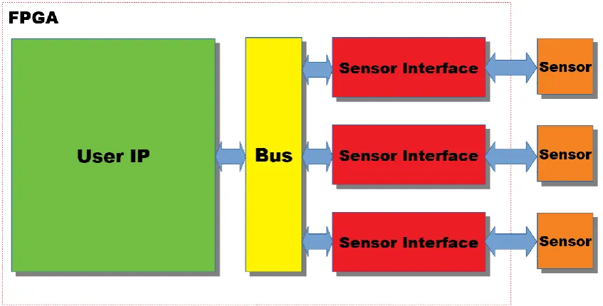
[image:10.595.86.510.448.663.2]framework will be located within this project because it will influence certain design choice made later on. The layout used for the main project is shown in Figure 5, the sensor interface is the focus of this thesis.
10 The layout consists of four parts:
Sensor
Represents the sensors and actuators connected to framework of the main project. Sensor interface
The sensor interface is responsible for the communication between the sensors and actuator and the bus. It converts data from the bus to something the sensor can use and the other way around. The sensor interface is going to be implemented as a framework and is the focus of this thesis.
Bus
Guides the data from the User IP to the correct sensor interface User IP
The user IP is responsible for the functional behaviour. It is responsible for reading the sensor data and controlling the corresponding actuator, its behaviour should be fully deterministic.
2.5 GOAL
The goal of the project is to create framework which consists of a set of building blocks which can be combined to create sensor/actuator interfaces for FPGAs. The designs made with these blocks should be easily analysable and must guarantee deterministic behaviour at all times. To describe the blocks in hardware the Clash-language is used. The design should be as small as possible in terms of hardware since they are going to be implemented on a FPGA.
2.6 DESIGN PROCESS
11 3 DESIGNING FRAMEW ORK
3.1 SENSOR INTERFACE IN DETAIL
The sensor interface is explored in more detail to get a better idea on what the sensor interface does and how to build a framework for it. As said before the sensor interface is responsible for translating the communication between the sensor and user IP. This process is split up into four different blocks to make analysis easier but also to make it better suitable for a framework (Figure 6).
Figure 6: Sensor Interface
As can be seen from the figure the sensor interface will be implemented as a pipeline where each block will have its own functionality as described below:
The Communication Interface is responsible for translating the sensor/actuator
protocol (SPI, I2C, UART, …) to something that can be used by the sensor driver.
The Sensor Driver is responsible for communicating with the sensor/actuator and
initializing the sensor if necessary. The sensor driver handles commands from the user IP and sends sensor data back.
The Synchronisation is responsible for handling the communication between
different clock domains. Most of the times the clock frequency for a sensor is different from that of the users IP meaning some sort of synchronization is necessary.
The OI sampler acts as the front end of the sensor, it can receive input data for the
sensor and send output data to the user. This block compensates the variable delay of the synchronizer as will be explained later.
3.2 USE OF DATAFLOW IN FRAMEW ORK
12 in dataflow. The dataflow representation is used to show the hardware design is deterministic. If the theoretical approach is taken a dataflow design is made which is then represented in hardware. In this case the hardware is deterministic because it is derived from dataflow.
3.2.1 HARDW ARE PERSPECTIVE
The framework will consist of a set hardware blocks that can be combined to create different sensor interfaces. Each blocks will perform one of the functions shown in Figure 6 (Communication interface, driver, synchronizer or IO sampler). Different blocks can be made for each function to create different sensor interfaces. The blocks will be designed using the Clash-language meaning they are directly implemented in hardware. Taking this approach is useful since it gives a lot of flexibility with respect to hardware design choices. Being close to the hardware allows designing with optimization in mind which results in smaller and faster designs. The downside is that hardware is not deterministic by definition.
Proving the determinism is done by deriving a dataflow equivalent of each block. If the conversion is possible determinism is guaranteed.
From a user perspective this approach works as follows. The user connects different hardware blocks to create a sensor interface. The hardware blocks all have a
dataflow equivalent, these can be used by the user to do analysis on the design. 3.2.2 THEORETICAL PERSPECTIVE
The theoretical perspective starts with dataflow. The framework will consist of a set of dataflow nodes that can be combined to create a sensor interface. The nodes have a hardware equivalent that will be used to implement the design. This approach
guarantees determinism since it is based on dataflow. From a user perspective this solution will consist of a number of nodes, each with its own functionality. The user can combine these node to create a sensor interface. The hardware is a functional equivalent of the dataflow graph meaning the properties of the dataflow graph do also hold for the hardware.
3.3 DATAFLOW AND HARDW ARE
To use dataflow in combination with hardware a link between dataflow and hardware needs to be defined. This link is mainly based on how tokens are interpreted,
dataflow components get a different meaning based on the interpretation of tokens. Two different definitions are explained here called structural dataflow and functional dataflow.
3.3.1 STRUCTURAL DATAFLOW
13 like multiplexers and OR gates. The edges represent the wires between these
components. A wire in hardware does not have memory meaning an edge can only store one token at a time. All nodes have a delay of 1 clock cycle to guarantee new tokens each clock cycle.
The definition of data is lost with this approach, it is not known when a token contains data or nothing. For example, a node can produce data every 5 clock cycles, in dataflow this would mean it produces 4 tokens that contain “nothing” and one that contains the data. The contents of these 5 tokens cannot be observed meaning each one them could all be a “nothing” or “data”.
This representation can be used to prove that hardware is deterministic since it
guarantees a new signal every clock cycle. The graph doesn’t say anything about the deterministic behavior of the data itself. Data could still be outputted at random. 3.3.2 FUNCTIONAL DATAFLOW
When using the functional dataflow representation a token represent data in contrast to the structural dataflow where a token could be data as well as nothing. The nodes represent functions that use the input tokens to create an output. The time a node takes to do this must be multiple of 1 clock cycle to keep all nodes in sync with the clock. The edges can be seen as FIFOs in hardware, the size of the FIFO is limited meaning it can only hold a limited amount of data. This limitation is controlled by implementing backpressure, the number of tokens in the backpressure loop indicate the size. Adding backpressure makes the dataflow graph automatically strongly connected which means the dataflow graph is periodic. The delay of each of the nodes depend on their functional description in hardware, it should be at least one when it has internal storage. As a rule of thumb can be used: if a node has more than one input and output edge it has internal storage. The tokens only represent data meaning this representation can be used to prove the deterministic behavior of data. 3.4 FINAL SOLUTION
A decision needs to be made on how to design the framework. There are two choices that need to be made, is the structural or functional representation of hardware going to be used and is the framework going to be designed according to the theoretical or the hardware perspective.
Deciding whether to use the functional or structural representation of hardware is easy. The dataflow graph should proof the deterministic behaviour data resulting in the only possible representation, the functional one. This means nodes will represent functions and tokens represent data.
14 interchange them for a block with different functionality.
It turned out that this design approach results into problems. The freedom given while designing the hardware blocks resulted in nondeterministic designs. This made it necessary to formulate a design rule to prevent these design mistakes: “The output period or delay should not be influenced by nondeterministic inputs”. A second problem became clear later in the process, the timing. If one of the processes in the pipeline is slower than the blocks before it, the system would break since data can be lost. At first glance this was a problem that could be overcome by controlling the delay of the different blocks. The constraint limited the flexibility of the framework since certain combinations of blocks could result into timing problems. Besides the constraints for the framework itself there was also a problem with the processes after the IO sampler. It the processes after the sensor interface would be slower than then the output period of the sensor interface it would also result in data loss. To solve the delay problem a feedback system was added, each receiving block should indicate to the sending block if it is ready. The sending block is halted until the receiving block is able to process the data. Implementing these halt signals needed a redesign for each block.
The added complexity in terms of feedback reduced the hardware gain and prevented the relative ease with which blocks could be designed. Converting the hardware designs to dataflow often resulted in complex dataflow graph or no
dataflow graph at all. This made is hard to prove determinism and do analysis on the designs.
The first approach turned out to be more complex than initially thought, this was the reason to try the theoretical approach. Approaching the problem from dataflow perspective directly gave much better results. Analysis could be done beforehand since the dataflow calculation methods could be used. The timing problem was
covered by the backpressure required by the functional hardware representation. The added backpressure made the whole system become self-timed. The designing of nodes turned out to be easier than expected, the fact that dataflow rules should apply gave a good guidance during the design process.
In the end there is chosen to use the theoretical approach because it turned out to be better analysable and easier to implement.
The final solution for the framework uses a theoretical perspective, this means
designs will be made in dataflow which are later converted to hardware. The dataflow will use the functional representation of hardware meaning each node represents a function instead of a hardware components. The design from Figure 6 is converted accordingly as is shown in Figure 7.
15 The blocks from Figure 6 are converted to dataflow nodes. Each node is connected with backpressure to limit the storage on the edges.
3.5 IMPROVE PERFORMANCE FRAMEW ORK
The design from Figure 7 is not very efficient. With this design the nodes can only fire when both the previous and next node are finished. This structure limits parallel processing which can be shown by calculating the MCR:
𝑝𝑒𝑟𝑖𝑜𝑑 = max(𝑎 + 𝑏, 𝑏 + 𝑐, 𝑐 + 𝑑, 𝑎, 𝑏, 𝑐, 𝑑)
The output period equals the period of two nodes added.
By separating the communication aspect from the controller/functional part the parallelism can be improved (Figure 8). The ctrl node represent the functional part which is called controller from now on. The controller is responsible for processing incoming data and controlling the connected communication node. The
communication node is responsible for distributing incoming data to the next communication node and the controller. This node has a delay of 1 clock cycle because it has more than one input and output edge. The red arrows show how the data from the tokens goes through the system. As can be seen from the picture, data only goes in one direction. This choice is made to prevent forcing the input and output data to go through the same processing pipeline. Most of the times input data will require different processing than output data.
Figure 8: General layout framework
16 Figure 9: Dataflow general layout improved parallelism
The MCR is calculated for the new design:
𝑝𝑒𝑟𝑖𝑜𝑑 = max(𝑎 + 1, 𝑏 + 1, 𝑐 + 1, 𝑑 + 1, 2, 𝑎, 𝑏, 𝑐, 𝑑, 1)
The output period now equals the delay of one of the controller plus the delay of a communication node. It is assumed the controllers will have a delay bigger than the 1 clock cycle from the communication node. Based on this assumption it can be
17 4 IMPLEMENT FRAMEW ORK IN HARDWARE
4.1 FRAMEW ORK IN HARDW ARE
For the conversion from dataflow to hardware a standard procedure is used. There are two parts that need to be discussed, the backpressure and the nodes. Here the implementation of these two dataflow elements is explained.
4.1.1 BACKPRESSURE
Nodes/Edges/Backpressure.hs
Designing backpressure in hardware is a complex operation. The backpressure needs to store tokens (data) but cannot have a delay. To solve this problem there is started with a definition of tokens and edges in hardware. The choice is made to represent an edge as two lines, a data line and a control line. The control line is used for indicating tokens on the edge. When the control line is high it indicates there is a token present, when the line is low there is no token. The data inside the token is handled by the separate data line which sends the data in parallel. The values for the data and control line are stored at the output buffer of the node sending the token. When a node sends out a new token its output buffer is updated, the control signal is set to high to indicate the new token while the data line gets the new data. The backpressure is implemented with only one token in the loop, this means that new data can only be send when the previous data has been read.
When the backpressure edges are implemented in hardware as described above it would result in a working backpressure design (Figure 10). Keep in mind the nodes in the figure represent the hardware equivalent of a node as will be explained later.
Figure 10: Backpressure in hardware
The problem with this design is the following. When “Node A” sends a token because its input control line is high (high indicates a token), it has to wait at least one clock cycle before the input control signal is updated by “Node B”. This delay is the result of “Node B” having to update its output buffer. This means that “Node A” cannot read its inputs for one clock cycle after sending because they are not updated yet. This is not according to dataflow specifications and makes node design unnecessary complex. The nodes now need to have logic for their own behavior as well as well as logic for controlling the backpressure.
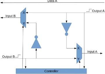
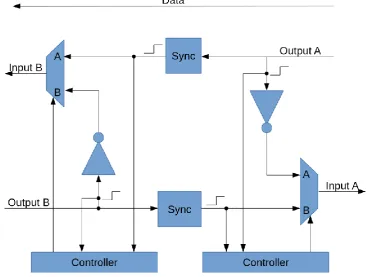
18 from having to worry about backpressure logic. This problem is solved by
implementing the backpressure as a state machine who switches between two circuit layouts, the state is controlled by the controller (Figure 11). The design shown here represents the backpressure between node A and node B (Figure 12). The state is switched when there is a signal edge on one of the input signals. The signal edges are used because it makes synchronization easier later on. The switching of state takes one clock cycle, to prevent strange behavior the input and output node should have at least a delay of one clock cycle. The inverters which connect the input to the output of a node act as a direct response to the input. It looks like the token on the incoming edge is consumed at the moment a token is put on the outgoing edge. This is not the exact behavior of dataflow since dataflow consumes tokens at the start of its execution. However, consuming the token at “firing” time doesn’t influence the dataflow behavior.
There are “signal edge” symbols shown next to the input lines, these indicate the signal is a signal edge instead of the signal itself. This line is high when the input signal changes and low when it equals its previous value. The switching of state is done by the controller according to the following rules:
➔ If State is X and there is an edge on output A the state goes to Y
[image:19.595.115.477.426.680.2]➔ If State is Y and there is an edge on output B the state goes to X
19 Figure 12: Backpressure between node A and node B
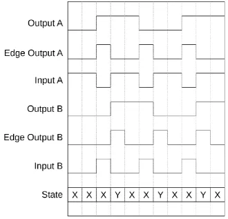
[image:20.595.132.463.225.542.2]The backpressure only communicate data in one direction as is shown by only one data line. An example shown in Figure 13 for dataflow graph of Figure 14.
Figure 13: Plot working backpressure
Figure 14: Example dataflow layout
4.1.2 NODES
20 while the “Wait” state is used for waiting on new input tokens. When in the “Fire” state the next state depends on the available input tokens. When there are tokens
available at all input edges (inputs are high) the next state is again the “Fire” state, if not the next state is “Wait”. When the node is in the “Wait” state and tokens are available at the inputs (inputs are high) the node goes to the “Fire” state. Every state execution takes one clock cycle meaning that every node has at least a delay of 1 clock cycle.
The state machine explained here is for a basic node. When the input tokens need to be processed states can be added before the “Fire” state. This means when tokens are available at all inputs the nodes goes through all the processing states finishing with the “Fire” state.
4.2 SYNCHRONIZATION
The framework needs to support synchronization between multiple clock domains. Some information is given with respect to calculating the Mean Time Between Failures for synchronizers and which designs are already available.
4.2.1 MEAN TIME BETWEEN FAILURES FOR SYNCHRONIZER
When communicating between different clock domains there is a change that data is corrupted due to the metastability of flip flops. This happens when the receiver reads the input data just before or just after it has been changed. How much time depends on the setup and hold times of the flip flops used. It cannot be guaranteed that metastability will never happen since the 2 clock domains are asynchronous. The only way to say something about the reliability of this communication is by calculating the chance an error will happen. There are different methods found on the internet, this one is chosen because of it is well documented (Wellheuser, 2018) (Patharkar, 2015) (blendics, 2018).
The chance a flip flop is metastable after a period tR is given by:
𝑃𝐹 = 𝑃𝐸∗ 𝑃𝑆
Where
𝑃𝐸 = 𝐶ℎ𝑎𝑛𝑐𝑒 𝑜𝑓 𝑒𝑛𝑡𝑒𝑟𝑖𝑛𝑔 𝑚𝑒𝑡𝑎𝑠𝑡𝑎𝑏𝑖𝑙𝑖𝑡𝑦
𝑃𝑆 = 𝐶ℎ𝑎𝑛𝑐𝑒 𝑜𝑓 𝑏𝑒𝑖𝑛𝑔 𝑚𝑒𝑡𝑎𝑠𝑡𝑎𝑏𝑙𝑒 𝑎𝑓𝑡𝑒𝑟 𝑡𝑅
PE is determined by calculating the chance that the edge of the output clock is inside the danger zone of the flip flop (T0). This is the period where the propagation delay of the flipflop is higher than the clock. The probability is calculated by dividing T0 by the clock period tC.
𝑃𝐸 =
𝑇0
𝑡𝑐 = 𝑓𝑐𝑇0
21
𝑓𝑐 = 𝑜𝑢𝑡𝑝𝑢𝑡 𝑓𝑟𝑒𝑞𝑢𝑒𝑛𝑐𝑦 (𝐻𝑧)
𝑡𝑐 = 𝑐𝑙𝑜𝑐𝑘 𝑝𝑒𝑟𝑖𝑜𝑑 (𝑠)
𝑡𝑠𝑢 = 𝑠𝑒𝑡𝑢𝑝 𝑡𝑖𝑚𝑒 (𝑠)
𝑡ℎ = ℎ𝑜𝑙𝑑 𝑡𝑖𝑚𝑒 (𝑠)
The metastability of a flip flop after tR seconds is given by:
𝑃𝑆 = 𝑒− 𝑡𝑅
𝜏
Where
𝑡𝑅 = 𝑟𝑒𝑠𝑜𝑙𝑢𝑡𝑖𝑜𝑛 𝑡𝑖𝑚𝑒
𝜏 = 𝑎 𝑡𝑖𝑚𝑒 𝑐𝑜𝑛𝑠𝑡𝑎𝑛𝑡, 𝑓𝑙𝑖𝑝 𝑓𝑙𝑜𝑝 𝑠𝑝𝑒𝑐𝑖𝑓𝑖𝑐
The resolution time is the time available for the signal to become stable. This means it is a full clock cycle minus constant delays.
𝑡𝑅 =
1
𝑓𝑐 − 𝑡𝑝𝑟𝑜𝑝− 𝑡𝑠𝑢
When both probabilities are combined it results in the following formula:
𝑃𝐹 = 𝑃𝐸𝑃𝑆 = 𝑓𝑐 ∗ (𝑡𝑠𝑢− 𝑡ℎ) ∗ 𝑒−
1
𝑓𝑐−𝑡𝑝𝑟𝑜𝑝−𝑡𝑠𝑢
𝜏
To get the failure rate the changing frequency of the input needs to be known. Assume the input changes with a rate fd, then the failure rate becomes:
𝜆 = 𝑓𝑑𝑃𝐹 = 𝑓𝑑𝑓𝑐 ∗ (𝑡𝑠𝑢− 𝑡ℎ) ∗ 𝑒− 1
𝑓𝑐−𝑡𝑝𝑟𝑜𝑝−𝑡𝑠𝑢
𝜏
The failure rate can be used to calculate the mean time between failures (MTBF) as follows
𝑀𝑇𝐵𝐹 =1 𝜆 =
𝑒
1
𝑓𝑐−𝑡𝑝𝑟𝑜𝑝−𝑡𝑠𝑢
𝜏
𝑓𝑑𝑓𝑐 ∗ (𝑡𝑠𝑢− 𝑡ℎ) = 𝑒𝑡𝜏𝑅
𝑓𝑑𝑓𝑐∗ 𝑇0
22
𝑡𝑝𝑟𝑜𝑝 + 𝑡𝑠𝑢 = 1.3 𝑛𝑠
𝑇0 = 𝑡𝑠𝑢− 𝑡ℎ = 2.05 𝑛𝑠
𝜏 = 0.4 𝑛𝑠
To improve the MTBF it is possible add an extra flip flops in series, by doing so the performance is improved since the resolution time is doubled.
𝑃𝐹 = 𝑃𝐸∗ 𝑃𝑆1 ∗ 𝑃𝑆2
𝑀𝑇𝐵𝐹 = 𝑒
𝑡𝑅
𝜏
𝑓𝑑𝑓𝑐𝑇0∗ 𝑒
𝑡𝑅
𝜏 = 𝑒 2𝑡𝑅
𝜏
𝑓𝑑𝑓𝑐𝑇0
Multiple flipflops can be added to improve the MTBF even more, this is at the cost of communication speed since more cycles are needed to transport one message from one to the other clock domain. The MTBF for “x” number of flip flops is:
𝑀𝑇𝐵𝐹 == 𝑒
𝑥𝑡𝜏𝑅
𝑓𝑑𝑓𝑐𝑇0
As both the formulas show the MTBF will increase when the input or output
frequency decreases, this can be explained by the fact that the flipflops have more time to become stable.
4.2.2 SYNCHRONIZER SOLUTIONS
There are a number of different designs available for synchronizing data between 2 clock domains. The different layouts mentioned here vary in complexity (Sachin Hatture, 2015) (Tejas, Amit, & Divyanshu, 2018). These designs are mainly used when the two frequencies that need to be synchronized aren’t a multiple of each other. The synchronizer designs are implemented to improve the Mean Time Between Failures (MTBF). Since there is chance data is read by the receiving domain when it is not yet stable.
The first design is simply 2 flipflops in series (Figure 15).
Figure 15: Dual flip synchronizer
This circuit useful since it uses minimal hardware to make multidomain
23 when a signal has arrived in the other domain. The design is also not useful for
synchronizing multiple bits since it will decrease the MTBF drastically. Correct operation of this design requires the input signal to be constant during
synchronization.
To improve the synchronization of multiple bits the following solution is used (Figure 16).
Figure 16: Dual flip flop data synchronizer
This solution is based on the 2 flip flop synchronizer but has a separate
communication line for data. The data line has twice as long to become stable compared the synchronization line. To make this solution work the data line should remain constant until the data has been read on the receiver side. Since there is no feedback this is hard to determine. This problem can be circumvented by making the clock frequency of the receiver domain at least twice as high as the clock of the sender domain.
24 Figure 17: Synchronizer with feedback
This design send a signal to the receiver, this signal is then returned to the sender. During this period a busy signal is kept high at the sender side to indicate no new signal can be send. This solution solves the feedback problem at the cost of more hardware. It does not allow to send data since it only has one communication line. Two other designs found improve on the data communication aspect. The first solution adds data lines to a sort of handshake design, the last solution uses a FIFO buffer as communication. A FIFO is the most reliable way of communication but does require a lot of hardware. The best trade-off is the handshake protocol with data communication abilities.
4.3 FRAMEW ORK CONTENTS
The framework is going to consist of a number of dataflow nodes that have a hardware equivalent. Multiple nodes have been designed to create a first basis for the framework. Each node is designed in a number of steps:
1. Design a dataflow node of the function that is going to be added
2. Convert the designed node to hardware design (explanation shown in appendix A.4)
25 4.3.1 COMMUNICATION NODES
As explained before, these nodes are responsible for sending the data through the system. They will be used in combination with a controller. A number of different nodes are designed as is shown here:
4.3.1.1 INPUT NODE
Nodes/Basic/NodeInput.hs
The input node reads data from its input and outputs it to the controller (Figure 18).
Figure 18: NodeInput
4.3.1.2 OUTPUT NODE
Nodes/Basic/NodeOutput.hs
The output node read data from the controller and outputs it to the rest of the system (Figure 19).
26
4.3.1.3 NORMAL NODE
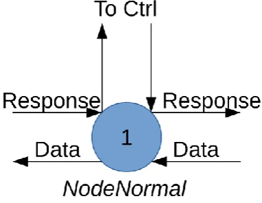
Nodes/Basic/NodeNormal.hs
The normal node read input data and sends it to the connected controller, at the same time it reads the previous controller value and sends it to the output (Figure 20).
Figure 20: NodeNormal
4.3.1.4 BLOCKING NODE
Nodes/Basic/NodeBlock.hs
[image:27.595.201.392.186.334.2]The blocking node blocks its input after an output, it is enabled again when the controller returns a signal (Figure 21). The controller should be of the type delay.
Figure 21: NodeBlock
4.3.2 CONTROLLERS
Controller manipulate the input data and then output them again. A controller should be used in conjunction with a communication node. A number of pre-made controllers is shown here. A structured way of creating custom controllers is explained in
27
4.3.2.1 SPI
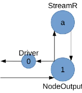
Nodes/Controllers/SPI/Stream.hs Nodes/Controllers/SPI/StreamR.hs
The SPI controllers are used to communicate with a SPI interface. There are two design:
Stream: Does not pull CS high after each message
StreamR: Pulls CS high after every message
4.3.2.1.1 DATAFLOW DESIGN
The dataflow model can be found in Figure 22.
Figure 22: Controller SPI
The initial dataflow design has an unknown execution time a, the value for a is determined by the implementation in Clash. The Clash implementation has a delay equal to x+1 where x represents the message size.
4.3.2.1.2 HARDWARE DESIGN
To understand where the x+1 delay for the node is coming from the underlying hardware needs to be known. The controller reads data from its input and puts it in an internal buffer, the first bit is directly written to the sensor since it is unnecessary to store. The next x (depending on message size) clock cycles data is read from the sensor and put in the buffer while data from the buffer is written to the sensor. When the last bit is written the full buffer is outputted together with the last bit from the sensor making the output complete (Figure 23).
28 When no data is available at the input of the node the controller is halted and the sensor clock is turned off until new data is available.
4.3.2.2 NODE DELAY
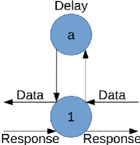
Nodes/Delay/Delay.hs
The delay node is a controller that adds a delay between its input and output. It can be used in combination with the nodeBlock to block the input for a number of clock cycles. The dataflow looks like Figure 24.
Figure 24: Delay
4.3.3 OTHERS
This node could be categorized as a controller or a communication node since it doesn’t store tokens. It converts an incoming token outputs it directly hence the 0 delay.
4.3.3.1 SLICE TOKEN
Designs/SliceToken.hs
The slice token node can be used to make the length of a token in number of bits smaller, this can be useful for getting rid of useless data. The node can be
implemented with zero delay since cutting of bits in hardware is done by not connecting wires.
Figure 25: Dataflow SliceToken
29 4.4 FRAMEW ORK IMPLEMENTATIONS FOR SENSOR INTERFACE
These are implementations made with framework nodes explained above. These designs are made to create a sensor interface. In some cases a custom parts are added, the choice to include these parts will be explained when this is the case. 4.4.1 COMMUNICATION INTERFACE
4.4.1.1 SPI INTERFACE
Designs/SPIinterface.hs
This design is made to make working with SPI easier, the design needs as inputs an SPI controller type (Stream, StreamR) and the type of communication node. The design then automatically generates the correct layout of nodes.
4.4.2 SENSOR DRIVER
No specific implementations have been designed as sensor driver. 4.4.3 SYNCHRONIZATION
There are cases where a design needs multiple clock domains, for example when communicating with a sensor. Sensors do often run at lower clock speed then the logic using the sensor data. There is the option to use oversampling for this problem to get rid of the second clock but this needs hardware to convert the sample data. The higher clock speed used for oversampling will also limit the flexibility in placing the hardware on the FPGA, for lower clock speeds wires can be longer giving the FPGA more freedom in placing the different hardware components. To communicate between two clock domains synchronization is needed. Two designs are shown, one in case the two frequencies are multiples and one in the case they are not. Keep in mind that the execution times are worst case since they depend on the distance between the edges of the two clocks. This means that the output period of a
synchronizer is variable and not deterministic. The IO sampler that will be explained later can be used to compensate the variability.
4.4.3.1 SYNCHRONISATION: FREQUENCIES OF BOTH DOMAINS IS MULTIPLE
Designs/SyncMult.hs
30
𝑅𝑓 =
𝑓𝑖𝑛
𝑓𝑜𝑢𝑡 =
1 𝑑𝑖𝑛
1 𝑑𝑜𝑢𝑡
= 𝑑𝑜𝑢𝑡 𝑑𝑖𝑛
𝑑𝑜𝑢𝑡 = 𝑝𝑒𝑟𝑖𝑜𝑑 𝑜𝑓 𝑐𝑙𝑜𝑐𝑘 𝑜𝑢𝑡 (𝑠)
𝑑𝑖𝑛 = 𝑝𝑒𝑟𝑖𝑜𝑑 𝑜𝑓 𝑐𝑙𝑜𝑐𝑘 𝑖𝑛 (𝑠)
𝑅𝑓 = 𝑓𝑟𝑒𝑞𝑢𝑒𝑛𝑐𝑦 𝑟𝑎𝑡𝑖𝑜
There are two problem that need to be overcome. First is the synchronizing from the fast to the slow clock domain, the sending node needs to halt until the receiving domain has processed the data. The second problem arises when synchronizing from a slow to a fast clock domain, the node in the fast clock domain can read the same input signal multiple times since the output node updates its output signal too slow.
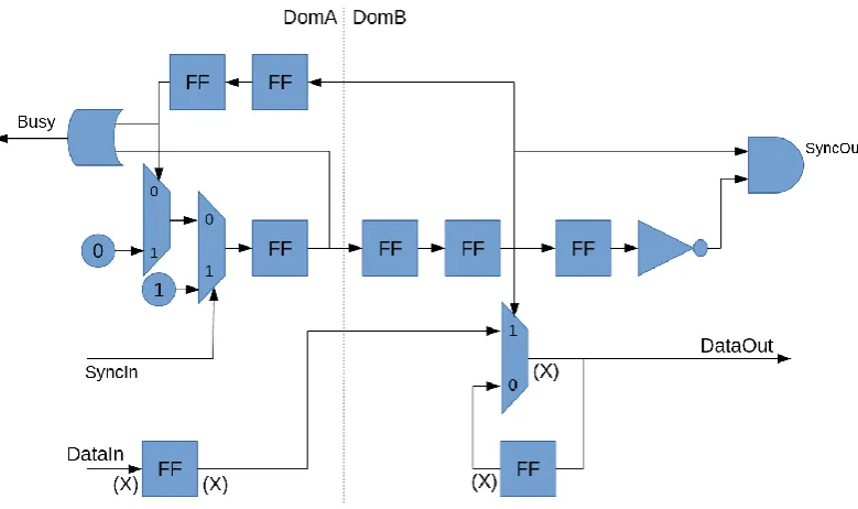
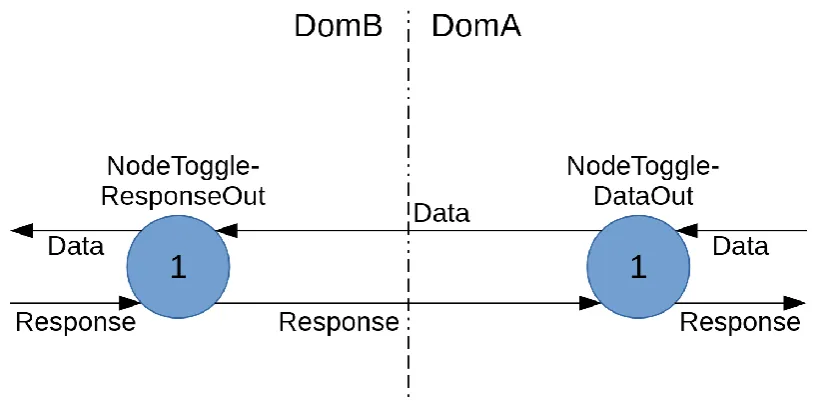
The synchronization from the fast to the slow domain has already been covered by the backpressure since it halts the sending node. The other way around is a bit more difficult, it is solved as follows. The synchronization uses a custom node which toggles its output instead setting it high or low, this in combination with the
[image:31.595.94.502.441.646.2]backpressure design explained earlier prevents the system from reading the same input multiple times. The layout is shown in Figure 26. No synchronization flip flops are needed since there is no metastability.
Figure 26: Synchronization multiple
The backpressure design should run at the highest frequency of the two synchronizer frequencies to assure correct edge detection.
31
𝑇ℎ𝑟𝑜𝑢𝑔ℎ𝑝𝑢𝑡𝑠𝑦𝑛𝑐𝑀𝑢𝑙𝑡= 𝑑𝑖𝑛+ 𝑑𝑜𝑢𝑡
𝑑𝑜𝑢𝑡 = 𝑝𝑒𝑟𝑖𝑜𝑑 𝑜𝑓 𝑐𝑙𝑜𝑐𝑘 𝑜𝑢𝑡 (𝑠)
𝑑𝑖𝑛 = 𝑝𝑒𝑟𝑖𝑜𝑑 𝑜𝑓 𝑐𝑙𝑜𝑐𝑘 𝑖𝑛 (𝑠)
The maximum delay from input to output is:
𝐷𝑒𝑙𝑎𝑦𝑠𝑦𝑛𝑐𝑀𝑢𝑙𝑡 = 𝑑𝑖𝑛+ 𝑑𝑜𝑢𝑡
𝑑𝑜𝑢𝑡 = 𝑝𝑒𝑟𝑖𝑜𝑑 𝑜𝑓 𝑐𝑙𝑜𝑐𝑘 𝑜𝑢𝑡 (𝑠)
𝑑𝑖𝑛 = 𝑝𝑒𝑟𝑖𝑜𝑑 𝑜𝑓 𝑐𝑙𝑜𝑐𝑘 𝑖𝑛 (𝑠)
4.4.3.2 SYNCHRONISATION: FREQUENCIES OF BOTH DOMAINS IS NO MULTIPLE
Designs/SyncNoMult.hs
When the clocks are not a multiple of each other synchronization becomes more difficult, it can never be guaranteed that the clock edges are in sync.
The already existing designs explained earlier are hard to combine with the dataflow format used. There has been decided to use the same design as in Figure 26. The communication between the two domains is extended with a dual flip synchronizer (Figure 27). The flip flops are indicated by the circles with c and d in them. The value for c and d represent the number of flip flops in the synchronizer.
Figure 27: Synchronizer frequencies aren't multiples
For the synchronization in both directions the normal flip flop design is used (Figure 15). The data itself is synchronized separately based on (Figure 16), the only
32 respond which is always larger than time it needs to become stable. The
[image:33.595.112.480.140.417.2]backpressure is a custom designed since it had to be split up to make room for the synchronizer flip flops Figure 28.
Figure 28: Back pressure design for synchronization
The minimum throughput of this synchronizer can be calculated by determining the maximum period of the design:
𝑇ℎ𝑟𝑜𝑢𝑔ℎ𝑝𝑢𝑡𝑀𝑖𝑛𝑠𝑦𝑛𝑐𝑁𝑜𝑀𝑢𝑙𝑡 = (𝑑 + 1) ∗ 𝑑𝑖𝑛+ (𝑐 + 1) ∗ 𝑑𝑜𝑢𝑡
The maximum delay of the design is
𝐷𝑒𝑙𝑎𝑦𝑠𝑦𝑛𝑐𝑁𝑜𝑀𝑢𝑙𝑡= 𝑑𝑖𝑛+ (𝑐 + 1) ∗ 𝑑𝑜𝑢𝑡
The MTBF is calculated for this design and can be found in appendix A.2.
4.4.3.3 SMART SYNC
Designs/SmartSync.hs
The smart sync design automatically determines which synchronization solution is best based on the given input frequencies. It can choose between no
33 4.4.4 IO SAMPLER
4.4.4.1 FLOW GATE
Designs/FlowGate.hs
[image:34.595.229.368.267.411.2]This design is based on the NodeBlock communication node, it can be combined with different delay controllers and by doing so influence its behavior. At this moment there is only one option which is called “Delay”, this option adds a Delay controller to the communication node so the input blocked for a number of clock cycles after each input. The design compensates for the extra delay added by the communication node. (Figure 29).
34 5 RESULTS
The framework will be tested in two steps:
➔ First all components of the framework will be tested separately. This includes both the nodes and the designs made with these nodes, like the synchronizer.
➔ Next the components of the framework are used to build a interface for a sensor. This is done to show that the framework can be used to build a deterministic interface.
5.1 TEST PROCESS
5.1.1 TEST BOARD
The FPGA board that is going to be used for testing is the Zybo-Z20 from Digilent. This board is equipped with a Zynq-7010 FPGA from Xilinx. All Digilent boards make use of a standard interface called PMOD, this interface is mainly used for connecting peripherals like sensors and actuators. The PMOD interface is called a standard but still uses 3 different pin layouts (1 x 6, 2 x 6 and 2 x4). Digilent provides a collection of devices that can be connected to the PMOD interface, these vary from displays to light sensors. Most of the devices are provided with an example code, sometimes this is only in C, other times also VHDL or Verilog. The official PMOD interface supports four protocols: SPI, GPIO, I2C and UART. The four communication protocols
supported by PMOD are very common.
5.1.2 TEST PROCESS INDIVIDUAL COMPONENTS
The individual components of the framework will be tested separately to verify that they are working correctly. These tests will be done by comparing the output of each of the individual components to a unique test vector. These test vectors are designed in such a way that most input to output combinations of a component are covered. The first tests will be done in the simulation environment of Clash. When the
simulations in Clash are successful the code will be converted to Verilog. The FPGA programming software Vivado is then used to simulate the Verilog code, the results are compared to the results from Clash. When this works the implementation for each component will be generated to get an idea of the hardware footprints, these
footprints are given in LUTs and flipflops.
5.1.3 TEST PROCESS IMPLEMENTATION
35 tool. If the simulations are successful the code is converted to VHDL and tested in Vivado. The output period of these simulations is determined and compared to their theoretical value. Next the design in implemented on the FPGA, it will be added as an AXI peripheral so the output can be read out by a CPU and displayed. The output signal indicating new data is connected to an output pin so the output period can be compared to the theory. The last step is checking the size of the design in number of flip flops and LUTs
5.1.3.1 SENSOR
The sensor used is a Digilent PMOD light-sensor. This is a sensor with an SPI interface that sends out 2 bytes of data every time the chip select goes from high to low. The 2 bytes consist of 3 zeros, then 8 bits of data followed by 4 zeros (Figure 30). The 15 bits are collected by the driver, the driver cuts off the zeros and then puts the data on the output. The sensor has an operating frequency between 1 MHz and 4 MHz. There is chosen to use an SPI sensor instead of an I2C, UART or GPIO because the other interfaces had
implementation problems. The implementation of I2C needs tri-state inputs and outputs for communication which cannot be implemented in Clash. The UART interface needs a clock which must be synchronised which is not possible is Clash unfortunately. A solution would be to do oversampling, if SPI was not easier to implement this interface would have been chosen. The last interface that could be used is GPIO, this is not used since it is too specific for each sensor which is not in line with a framework design.
Figure 30: Data layout light sensor
5.1.3.2 LAYOUT
The layout of the test setup will differ depending on the input and output frequencies. The Clash design automatically changes the layout depending on these frequencies. To guarantee the design fully works the three possible layouts will be tested
separately. These layouts are:
➔ Frequency of sensor and receiver are equal
➔ Frequency of sensor is multiple of the receiver frequency
36
5.1.3.2.1 DESIGN 1: FREQUENCIES ARE EQUAL
When the input and output frequency are equal, the synchronization step is not necessary, the dataflow is given in Figure 31.
Figure 31: Dataflow Lightsensor without synchronization
The IO sampler is left out since there is no synchronization so no variable delay. The SPI interface uses the streamR design, this design pulls CS high after every
message. This is necessary to have the sensor work correctly. The sensor itself only outputs data, this is why the communication node below the streamR SPI interface uses the NodeOutput design. The delay for the streamR controller equals the message size plus 1 which results in a delay of 16 cycles.
The output period can be determined by calculating the MCR, there are only three loops in this design to it is relatively easy to do.
𝑀𝐶𝑅 = max(16 + 1, 16, 1) = 17 𝑐𝑦𝑐𝑙𝑒𝑠
5.1.3.2.2 DESIGN 2: FREQUENCIES ARE MULTIPLES
[image:37.595.224.366.144.305.2]The next test uses two frequencies that are multiples. The sensor frequency is set to 2 Mhz, the frequency of the user IP is set to 100 Mhz. The design that results from these frequencies is shown in Figure 32.
37 The design consists of three components: The SPI interface, the synchronization and the IO sampler. The delay for the streamR controller is the same as for equal
frequencies so 16 cycles.
The synchronization uses the design for frequencies that are a multiple of each other. The last component is the IO sampler. The IO sampler is responsible for correcting the variable delay of the synchronizer so the output of the dataflow is deterministic. The period of the IO sampler should be equal or higher than the MCR of the rest of the sensor interface.
The delays for the nodes are given in number of clock cycles for their specific domain. The delays are corrected by dividing them by the frequency ratio given below so all delays are given in number of output clock cycles.
𝑅𝑓 =𝑓𝑠𝑒𝑛𝑠𝑜𝑟 𝑓𝑢𝑠𝑒𝑟𝐼𝑃 =
2 𝑀𝐻𝑧 100 𝑀𝐻𝑧 =
1 50
The corrected dataflow graph is shown in Figure 33. The different loops in the dataflow graph are marked.
Figure 33: Dataflow light sensor when frequencies are multiples, corrected
The value for b is still unknown. It can be calculated by using the property that the output period (L5) should equal the MCR of the rest of the dataflow:
𝑀𝐶𝑅𝑜𝑡ℎ𝑒𝑟 = 𝐿5 = 𝑏 + 1 = 𝑚𝑎𝑥(𝑙1, 𝑙2, 𝑙3, 𝑙4)
The periods of the designs are:
𝑙1 = 16 + 1
𝑅𝑓 = 850
𝑙2 =
1 + 1
𝑅𝑓 = 100
𝑙3 = 1 + 1 𝑅𝑓 = 51
38 When these values are filled in it results in a value for b:
𝑏 = 𝑚𝑎𝑥(850,100,51,2) − 1 = 849
As can be seen from the results the SPI interface is the slowest part of the design. The design will generate an output with a period of 850 clock cycles.
5.1.3.2.3 DESIGN 3: FREQUENCIES ARE NO MULTIPLE
The last case is if the frequencies used are no multiple. The frequency for the userIP is set to 101 MHz, the sensor still used 2 MHz. The new design will look like Figure 34.
Figure 34: Dataflow Light sensor, frequencies are no multiples
As can be seen, in this case the synchronizer for frequencies that aren’t a multiple is used. The variables b and c represent the number of flip flops between the two nodes, both b and c are set to two since there is no option in the code yet to set number of flip flops. There is started with the calculation of a.
The value for “a” equals the 16 clock cycles from before since the message size did not change.
The clock cycles delay in the sensor domain are corrected in the same way as was done for the previous solution. The frequency ratio is used to convert the delays in the sensor domain to the output domain.
𝑅𝑓 = 𝑓𝑠𝑒𝑛𝑠𝑜𝑟 𝑓𝑢𝑠𝑒𝑟𝐼𝑃 =
2 𝑀𝐻𝑧 101 𝑀𝐻𝑧 =
2 101
39 Figure 35: Dataflow light sensor when frequencies aren't multiples, corrected
The value for d is still unknown but can be calculated by using the property that the output period (L5) should equal the MCR of the rest of the dataflow:
𝑀𝐶𝑅𝑜𝑡ℎ𝑒𝑟 = 𝐿5 = 𝑑 + 1 = 𝑚𝑎𝑥(𝑙1, 𝑙2, 𝑙3, 𝑙4)
The periods of the designs are:
𝑙1 =
16 + 1
𝑅𝑓 = 858.5
𝑙2 = 1 + 1
𝑅𝑓 = 101
𝑙3 = 1 + 2 +
2 + 1
𝑅𝑓 = 154.5
𝑙4 = 1 + 1 = 2
When these values are filled in it results in a value for d:
𝑑 = 𝑚𝑎𝑥(858.5, 101, 154.5, 2) − 1 = 857.5
The ceil value for d is used since half clock cycles do not exist.
𝑐𝑒𝑖𝑙(𝑑) = 858
The slowest loop is again the SPI interface. The output period equals in this case 859 clock cycles.
The MTBF is calculated to check if the synchronizer is reliable enough. A good target value for MTBF could not be found so it is set to 1000 years. The calculation for this setup resulted in a MTBF of:
40 This is much higher than the required 1000 years, the full calculation can be found in appendix A.5.
5.1.3.3 TEST ON FPGA
The last step is to test the design on the FPGA, this will be done by connecting it to the AXI bus and communicate over UART. The bit indicating new data can be analyzed with the build in logic analyzer of Vivado, the period of this signal should equal (depending on design).
𝐹𝑟𝑒𝑞𝑢𝑒𝑛𝑐𝑖𝑒𝑠 𝑎𝑟𝑒 𝑚𝑢𝑙𝑡𝑖𝑝𝑙𝑒: 850 𝑠𝑎𝑚𝑝𝑙𝑒𝑠
41 5.2 TESTING FRAMEWORK
5.2.1 TESTING INDIVIDUAL COMPONENTS
[image:42.595.73.526.195.752.2]All the components inside the framework are tested in Clash as well as in Vivado, the results are given in Table 1.
Table 1: Results testing components
NODE NAME SETTINGS CLASH
SIM
VIVADO SIM
SIZE
BACKPRESSURE Constant Success Success 1 LUT
3 REGISTER
NODEINPUT Input: 8 Bit
Output: 8 Bit
Success Success 2 LUT
10 REGISTERS
NODEOUTPUT Input: 8 Bit
Output: 8 Bit
Success Success 2 LUT
11 REGISTERS
NODENORMAL Input: 8 Bit
Output: 9 Bit
Success Success 2 LUT
20 REGISTERS
NODEBLOCK Input: 8 Bit
Output: 8 Bit
Success Success 2 LUT
11 REGISTERS
DELAY Delay: 3 Success Success 2 LUT
5 REGISTERS
SYNCMULT Input: 8 Bit
Output: 8 Bit
Success Success 7 LUT
23 REGISTERS
SYNCNOMULT Input: 8 Bit
Output: 8 Bit
Success Success 8 LUT
30 REGISTERS
FLOWGATE Input: 8 Bit
Output: 8 Bit
Delay: 4
Success Success 5 LUT
18 REGISTERS
STREAM Input: 8 Bit
Output: 8 Bit
Success Success 14 LUT
25 REGISTERS
STREAMR Input: 8 Bit
Output: 8 Bit
Success Success 14 LUT
42 5.2.2 TESTING IMPLEMENTATION
The three different layouts for the light sensor interface are tested separately.
5.2.2.1 FREQUENCIES ARE EQUAL
5.2.2.1.1 SIMULATION
The simulation in clash for the interface with equal frequencies is ran successfully. The clash-language is converted to VHDL and tested in Vivado. The time stamps where new data arrives are 80,003 ms, 165,003 ms and 250,003 ms. The time between these results is 85 ms. The output frequency is 2 MHz meaning a period of 500 ns, this means the number of cycles between outputs is:
85000
0,5 = 170000 𝑐𝑦𝑐𝑙𝑒𝑠
The period should be 17 cycles which means the value from the simulation is 10000 times to high, when there is looked at the results in more detail it can be seen that a clock period takes 5 ms (smallest period without change), this is 10000 times too high. The difference is probably caused by the simulation clock which means the error is caused by the Clash compiler.
5.2.2.1.2 FPGA
The design is implemented on the FPGA, there is tested if the sensor is read out correctly. The output values cover the full range of the sensor so it can be assumed sensor is read out correctly.
Next the output period is tested to see if the output is periodic, the results are shown in Figure 36. Every pulse indicates new data, for periodic behavior the distance between the pulses should be equal.
Figure 36: Output signal indicating new data for the setup where the
frequencies for the sensor and userIP are equal. Each pulse indicates a new output, the period between the pulses is constant meaning the output is periodic.
The pulses are at sample times:
3, 20 ,37, 54, 71, 88, 105
43 The size of the design when implemented on a FPGA is:
45 REGISTERS, 20 LUT
5.2.2.2 FREQUENCIES ARE MULTIPLE
5.2.2.2.1 SIMULATION
The next design that is going to be tested is the one where frequencies are multiples. The IO sampler added is filled in by hand since it is not yet possible to let Clash do this. The period is determined by running the function for calculating the MCR before compilation, the result in then filled in. The function returns a MCR of 850 cycles which equals the value calculated earlier.
The clash simulation is ran successfully so the code is converted to VHDL. The simulation in Vivado shows outputs generated at: 85.203 us, 170.203 us, 255.203 us. The difference between these outputs is exactly 85.000 us. The output frequency equals 100 MHz which results in a period of 10 ns. With these values the output period can be calculated:
85000000
10 = 8500000 𝑐𝑦𝑐𝑙𝑒𝑠
The calculated output frequency is again a factor 10.000 too high. The graphs show that the clock period during simulation equals 100 us, this is about 10.000 times higher than the period calculated which explains the difference.
5.2.2.2.2 TEST ON FPGA
The simulations work correctly so the design can be implemented on a FPGA. The sensor is read out correctly meaning the sensor interface is working. Next the output is tested so see if it is periodic, the results are shown in Figure 37. Every pulse indicates new data, the distance between the pulses should be equal for periodic behavior.
Figure 37: Output signal indicating new data for the setup where the
44 The pulses are at sample times:
339,1189, 2039, 2889, 3739, 4589, 5439, 6289, 7139, 7989
The time between the samples are 850 samples meaning the output period equals the 850 cycles determined in the method.
The size of the final design is 100 REGISTERS, 40 LUT
5.2.2.3 FREQUENCIES ARE NO MULTIPLE
5.2.2.3.1 SIMULATION
The design where the 2 frequencies are not a multiple of each other is the most complex version. Again the output period is filled in by hand but should in this case equal 859 cycles. After the Clash simulation is ran successfully the code is converted to VHDL. The periodic is checked in Vivado, outputs are generated around:
85.349,62 ns, 170.399,21 ns, 255.448,8 ns. The difference between these times is 85.049,59 ns which means the output is periodic. The output frequency is 101 MHz meaning it has a period of 9,901 ns, this means the number of cycles between outputs is:
85.049.000,59
9,901 = 8590000 𝑐𝑦𝑐𝑙𝑒𝑠
This is again a factor 10.000 too high, the reason is most likely the same as for the previous result.
5.2.2.3.2 TEST ON FPGA
45
Figure 38: Output signal indicating new data for the setup where the
frequencies for the sensor and userIP are not a multiple of each other. Each pulse indicates a new output, the period between the pulses is constant meaning the output is periodic.
The pulses are at sample times:
830, 1689, 2548, 3407, 4266, 5125, 5984, 6843, 7702
The times between the pulses equals the 859 determined in the method. The size of the full layout is:
107 REGISTERS, 44 LUT
46 6 CONCLUSION
Designing a framework that has to deliver deterministic and real time designs is not an easy task. The first step taken in the design process was to use dataflow for analysis. Dataflow is useful because it is deterministic by definition and has a lot of analysis techniques already available. For the framework itself there where two options on how to design it. The first option was to design hardware blocks which could be combined to create a sensor interface. These designs would all have a dataflow equivalent to prove their deterministic behavior. The reason for choosing a hardware approach was the flexibility and ease of design. It turned out that this solution was much more complex than it initially seemed. There were problems with timing, dataflow conversion and doing analysis as a whole. This resulted in trying another approach. The second approach starts with dataflow. The framework is designed in dataflow and later converted to hardware. The framework itself consists of a set of dataflow nodes which can be combined by the user to create sensor interfaces. Each node has a hardware equivalent which is used to generate the design for a FPGA. The nodes are connected with backpressure to limit the number of tokens that can be stored on an edge and to make the whole system self-timed. This solution is much better analyzable at the cost of some flexibility. The designs made with the framework are automatically self-timed due to the backpressure, this makes designing simple since the timing problems are handled automatically.
Each node in the framework has been tested to check its functionality and to assure it behaves according to the dataflow rules. To test the deterministic behavior of the framework an interface for a SPI light sensor created. Its output signal is tested to see if it is deterministic and if it outputs realistic sensor readings.
The test done gave positive results, the output period was deterministic and the sensor was read out correctly. The amount of area used by the components is low, the test setup only used 118 FF and 58 LUTs. The small hardware footprint makes it realistic for implementation on a FPGA which has multiple thousands flip flops and LUTs available.
47 7 DISCUSSION AND FUTURE W ORK
There is a difference between the simulation done in Vivado and what is specified in Clash. The clock in Vivado is 10.000 times slower than the one implemented in Clash. This will not cause any problems since the relative speed difference between the clocks stays the same. However, it something that should be kept in mind when doing analysis on the simulation results.
The framework is at this moment limited in its functionality since there is only a small number of nodes available. The number of nodes should be increased in the future to add functionality to the framework.
The way nodes are connected at this moment is not as easy as it should be, all edges have to be connected by hand. In the future this should be simplified, an example of what the syntax could look like is:
𝑜𝑢𝑡𝑝𝑢𝑡 = 𝑛𝑜𝑑𝑒1 < −−> 𝑛𝑜𝑑𝑒2 < −−> (𝑛𝑜𝑑𝑒3 𝑖𝑛𝑝𝑢𝑡)
48 8 APPENDIX
A.1 COMMUNICATION PROTOCOLS
The PMOD interface uses four types of protocols. Each of these protocols is explained here.
A.1.1 SPI
SPI is a three+ wire communication protocol consisting of one master and 1+ slaves. Each slave adds an extra wire for communication in the form of a chip select. When the chip select is pulled low the slave is selected and the communication can start. The communication part of the interface consists of a clock, a mosi (master out, slave in) and a miso (master in, slave out). The word size and the operating frequency are not defined. The send and received message do not even have to be the same size. Most SPI slaves read on the falling edge to prevent problems with instable data. A.1.2 GPIO
GPIO stands for general purpose IO, it does not have a standard since it fully custom. This means nothing can be said about the communication protocol. A.1.3 I2C
The I2C communication interface only uses 2 wires, one clock and a data line. The protocol supports multiple masters and slaves. The maximum clock frequency is 100 kHz for normal speed and 400 kHz for full speed. In the default state both the clock and data line are kept high. To start communication first the data line is pulled low and then the clock. Next the clock is started and the address is send, this address can be 7 or 10 bits with an extra bit for reading or writing. In case of 7 bits one byte is send consisting of the address and the read/write bit. If the 10 bit address is used it will be send using two bytes. The byte starts with the code 11110 followed by 2 of the address bits and then the read/write bit. The next byte consists of the remaining 8 bits from the address. After each byte the receiver (slave in this case) will pull the data line low to indicate the message was received. All the message send with I2C have to be 8 bit.
A.1.4 UART