Faculty of Electrical Engineering, mathematics and Computer Science Supervisor: dr. ir. A.J. Annema
Switching Behavior of
AMLEDs
for Implementation in Opto-coupling
Devices on CMOS chips
K.P. De Meyere
Abstract
The use of Complementary Metal-Oxide Semiconductor (CMOS) chips is becoming more predominant in every day life, it being included in general appliances such as cell phones, televisions and tablets, to name a few. They are often used as control systems that op-erate at a much lower voltage than the system it controls and must work in electrical isolation from it. One method of doing so is to use an opto-coupling device that connects the two circuits using EM waves.
An opto-coupling device often has a substantial power consumption but a solution was proposed by A.J. Annema et al. to reduce this by using a Single Photon Avalanche Detector (SPAD) on the receiving end and an Avalanche Mode Light Emitting Diode (AMLED). The AMLED would have to emit a minimal amount of photons for it to be detected and can be turned o much faster and eciently than a forward LED. Using these components would lead to reduced power consumption and less interference on the rest of the system due to changing magnetic or electric eld.
The problem with the AMLED is that its switching behavior is not well dened and is most likely inuenced by dead time, a period of time in which there are no mobile carriers in the depletion layer.
The assignment was to investigate the existence and eect of dead time in a semiconduc-tor through simulations and experiments. Through the use of Sentaurus, a simulation program, and experimental set-ups it was attempted to nd the eects of the dead time. In the end there were no conclusive results as the simulation software ignored the prob-abilities of avalanching, making it avalanche every time possible and the experiments could not nd evidence of the dead time due to the large amount of charge injected by the saturation current of the transistor used.
Contents
Contents 2
List of Figures 3
1 Introduction 4
1.1 Theory . . . 4
2 Sentaurus Simulations 6 2.1 Avalanching in BJT Models . . . 6
2.1.1 Characterization of BJTs . . . 8
2.2 Avalanching in PN Junction . . . 11
2.2.1 Depletion Width . . . 11
2.2.2 Characterization of PN Junction . . . 13
2.3 Evaluation of Simulations . . . 14
3 Experiments 15 3.1 Repeated Avalanching Experiment . . . 18
3.2 Characterization of Transistors . . . 21
3.3 Evaluation of Experiments . . . 24
4 Conclusion 25 Bibliography 26 5 Appendices 27 5.1 Appendix A . . . 27
5.2 Appendix B . . . 31
5.3 Appendix C . . . 32
5.4 Appendix D . . . 33
5.5 Appendix E . . . 34
List of Figures
1.0.1 Dierent methods to communicate between circuits. . . 4
1.1.1 IV Curve of a standard diode . . . 5
2.1.1 A standard npn transistor design used as basis for simulation designs. . . 7
2.1.2 Two designs made in Sentaurus: (a) is half the structure of Figure 2.1.1 (b) replaces an STI with a gate. Units: cm−3 . . . 7
2.1.3 Close-up on varying distance. . . 8
2.1.4 IV Curves for the three dierent BJT designs with gate. . . 9
2.1.5 Impact Ionization within the structures. . . 10
2.1.6 Current through emitter node in the simulation when subjected to a 100MHz signal. . . 10
2.2.1 Standard BJT design with doping prole. . . 11
2.2.2 Carrier concentrations and electric potential for doping concentration 3. . 12
2.2.3 IV Curve for doping concentration 1019cm−3. . . 13
2.2.4 Transient sweep using a 10MHz on-o signal on the 1017 cm−3 junction. . 14
3.0.1 Circuit design featuring the possibility to actively quench the transistor. . 15
3.0.2 Simplied version of Figure 3.0.1. . . 16
3.0.3 ADS design of Figure 3.0.1 . . . 16
3.0.4 Contact denition of SOT23. . . 17
3.0.5 Preliminary IV Curve for the DC sweep of PMBT2369. . . 17
3.1.1 Voltage input vs voltage dierence across resistor R4, no bias. . . 18
3.1.2 Voltage input vs voltage dierence across resistor R4, 6.5V bias. . . 19
3.1.3 : Voltage dierences over resistor R4 with a) no bias and b) 6.5 bias. . . 20
3.2.1 IV curve for the PMBT2369 transistor at varying temperatures. . . 22
3.2.2 IV curve for the BSV52 transistor at varying temperatures. . . 23
3.2.3 IV curve for the BFM520 transistor at varying temperatures. . . 23
5.1.1 Sample coding for a BJT junction. . . 27
5.1.2 A design imported to Sentaurus Structure Editor. . . 28
5.1.3 Settings used in the simulations. . . 29
5.1.4 Signal dening code. . . 30
5.2.1 IV Curves for the three dierent BJT designs with gate. . . 31
5.3.1 Missing pulses graph. Could not be replicated. . . 32
5.4.1 Carrier concentrations and electrostatic potential for Doping 1. . . 33
5.4.2 Carrier concentrations and electrostatic potential for Doping 2. . . 34
5.5.1 Simulation Results using LT Spice. . . 34
1 Introduction
The use of Integrated Circuits (IC) on Complementary Metal-Oxide-Semiconductors (CMOS) is found in many of today's everyday appliances such as cell-phones, tablets and laptops. They are also found in many forms of control systems that can maintain high voltage functions while maintaining a low power output. In order to do so, these low voltage control systems have to interact with the devices through methods that keep both devices isolated.
Figure 1.0.1: Dierent methods to communicate between circuits.
Figure 1.0.1 contains symbolic representations for the dierent methods to communicate between two circuits. Circuits 1 and 2 are the signal modulating circuit and readout cir-cuit respectively. The one on the left consists of two decoupling capacitors that keep the DC components from traveling between the two circuits with the use of electric elds. The second method is to use a transformer to communicate between circuits 1 and 2 using a changing magnetic eld. The third option is to use electromagnetic (EM) waves emitted by an LED and detected using a photo-detector. Both magnetic and electric elds can inuence the circuits by inducing unwanted currents or voltage dierences. EM elds, on the other hand, do not inuence circuits and would produce the least amount of interference.
1.1 Theory
Figure 1.1.1: IV Curve of a standard diode
As stated before, the light emitted by the LED has to be sucient enough to be de-tectable by the photo-detector. This requires a substantial amount of forward voltage and will require a driving signal that can be modulated from 0 to this voltage, a power intensive signal to create. It is possible to make the LED switch intensities of which only one can be detected, but this would lead to a high amount of power loss as not all photons generated are used.
A possible solution is to use an Avalanche Mode LED (AMLED) that generates light when subjected to a suciently high reverse voltage. As can be seen in Figure 1.1.1, the benet of using an AMLED is that the power emitted increases substantially more than to the standard LED once the diode is in avalanching. If the signal is biased near the breakdown voltage, it should be possible to create photons with substantial energy to be detected, thus reducing power loss.
The switching behavior of an AMLED is limited by a few factors. The most promi-nent limiting factor is the dead time that arises after avalanching. The dead time denes the period in which the depletion layer is devoid of mobile charge carriers thus prohibiting the start of avalanching. [1] This limits the rate at which the AMLED can turn on and o and thus limiting the rate of data transfer. S. Cova et al. calculated a dead time of 1 µs for a standard SPAD [2] resulting in a maximum switching rate of 1MHz.
After each time the junction breaks down it has to be quenched. This can be done both passively or actively, depending on the circuit. A passive quenching circuit utilizes linear components such as resistors or capacitors to reset the electric elds within the semiconductor. An active quenching circuit uses the signal to quench the system as by changing the voltage drop over the diode. Active quenching is generally faster but it also more power intensive.
This won't be investigated in the report though, as this report will focus entirely on the avalanching behavior of silicon.
This work aims to investigate the implementation of opto-coupling on CMOS chips through the use of SPADs and AMLEDs. SPAD technology is advanced enough to not warrant further investigation, but AMLEDS require more attention. The switching behavior of avalanching diodes were simulated using Sentaurus and then tested through experimentation to determine the eect of dead time and the possible restrictions in signal transfer.
2 Sentaurus Simulations
In order to avoid wasting time and money, it is essential to model any design made be-forehand. This can best be done using the Sentaurus Workbench Tool, a program that allows for the design and simulation of custom semiconductor designs. Any theory can rst be tested using this program and will give insight on the behavior of the design. This, o course, is no substitute for an actual semiconductor to test on, but making real ones takes time and money thus it is most eective to rst design a semiconductor that appears to work as intended and to then test it physically.
A detailed description of the design process is given in Appendix A(5.1). The design for a standard BJT was provided by S. Dutta, a design that was subsequently altered to try and investigate the eects of changing various parameters. BJTs were investigated as it would provide a way to inject carriers into the depletion layer, decreasing the amount of dead time.
2.1 Avalanching in BJT Models
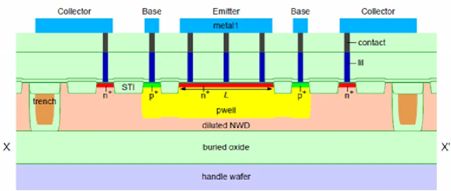
Figure 2.1.1: A standard npn transistor design used as basis for simulation designs.
This design is overly complex and simulating it would require a lot of time and pro-cessing power. It is, however, possible to simplify this structure. The design in Figure 2.1.1 is symmetrical, thus it is possible to reduce the structure to the mirrored design. By cutting the structure in half, there would be only 1 of each contact.
[image:8.595.73.520.76.266.2]Taking this into account, two designs were made, both of which follow the general prin-ciple of the provided example, but with slight variations, as seen in Figure 2.1.2.
Figure 2.1.2: Two designs made in Sentaurus: (a) is half the structure of Figure 2.1.1 (b) replaces an STI with a gate. Units: cm−3
occur near one of the STIs.
[image:9.595.211.385.204.277.2]The dierence between the two designs is the Shallow Trench Isolation (STI) between the emitter and the collector. The reason for this was to investigate its eect on the behavior of the system as well as to reduce the possibility of shorting the emitter and collector. This does, however, increase the distance the electrons would have to travel, thus decreasing the current gain and response time of the system.
Figure 2.1.3: Close-up on varying distance.
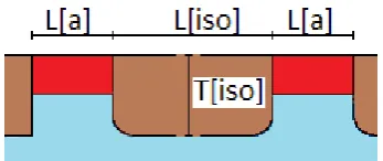
Based on that same principal, the distance between the collector and emitter (L[iso] in Figure 5) was made to be 0.3, 0.4 and 0.5 µm for the two designs, resulting in a total of 6 structures. The idea behind this was to investigate the eect if increasing the distance between the emitter and the collector. The isolated design also used the increased distance to provide something to compare the results of the gated designs with. These distances were chosen based upon the physical capabilities of the production of CMOS chips.
2.1.1 Characterization of BJTs
To make the BJT emit light it has to avalanche. This only happens when one of the junctions (base, collector, base-emitter, collector-emitter) is subjected to a high enough potential dierence, higher than their breakdown voltage. In this design, the emitter-base will be the subject of investigation as this is the junction that has the lowest breakdown voltage in physical transistors.
The switching behavior would be tested by modulating a signal around the breakdown voltage. An on-o signal with a DC oset slightly lower than the breakdown voltage will run through the BJT and cause the emitter-base junction to avalanche at regular intervals. When the signal is o the current through the emitter is near zero while it will be substantially larger when the signal is turned on.
The second option is to use the built in BreakAtIonIntegral command which forces the simulation to stop when breakdown occurs [3]. It is a neat tool provided by Sentau-rus which could shorten simulations signicantly. This is the method that was used as it provided the nicer graphs, ones that did not show erratic behavior past breakdown.
Figure 2.1.4: IV Curves for the three dierent BJT designs with gate.
The results were subsequently graphed onto a semi-logarithmic scale. Figure 6 shows the IV curves for the three dierent gated BJTs obtained using the BreakAtIonIntegral command. Each line features a sharp increase near the end indicating that it is approach-ing breakdown. Similar behavior was visible on the IV curve for the isolated design but it had one curve that looked as though it did not complete the simulation (there was no signicant current increase near breakdown). The reason for this was not found and every simulation consistently stopped at that point. See Appendix B (5.2) for the other IV plot of the isolated BJT.
Breakdown Voltage VBR per design: Gated 0.3 µm 6.40 V Gated 0.4 µm 8.26 V Gated 0.5 µm 8.78 V Isolated 0.3 µm 4.95 V Isolated 0.4 µm 7.61 V Isolated 0.5 µm 8.98 V
was biased just below these values and then simulated to go past the breakdown. If the frequency is low enough, every time the junctions are pushed into avalanche they should observe a signicant current change. If the frequency is too high there might be some pulses missing.
Figure 2.1.5: Impact Ionization within the structures.
Subsequently, the location of the breakdown is identied using Sentaurus Visual.
As seen in Figure 2.1.5, the impact ionization occurred primarily at the emitter junction with some ionization happening between at the other junctions and the substrate/base interface due to the dierences in doping levels. The emitter junction was avalanching and would release photons into the device and the surrounding isolation would act as waveguides.
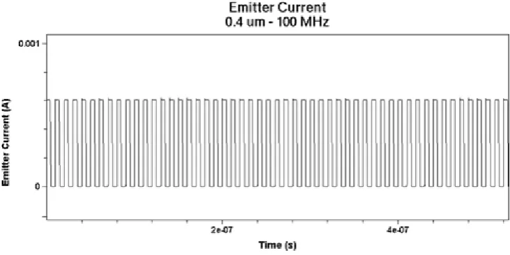
To test the switching behavior, a 100MHz signal was simulated to run through the design. This value is much higher than 1MHz and is therefore expected to be inuenced by the dead time. If the dead time were present, the junction should not avalanche at every instance and at some points no current should run through the emitter even though the voltage was past breakdown. These can be identied by missing pulses, irregularities in the current-time plot.
[image:11.595.115.481.542.725.2]The current through the emitter contact was in phase with the signal indicating that the emitter-base junction was avalanching. There were no irregularities, no missing pulses, though and this indicated that the dead time did not act on the system.
Every frequency used to drive the device resulted in a similar graph as Figure 2.1.6, a square wave with the same frequency as the signal and no missing pulses. This was the case for every design, both gated and isolated. There was a single instance where pulses went missing but the missing pulses were erratic and non-periodic. This graph was considered to be an outlier as it could not be replicated. See Appendix C(5.3) to see this graph.
The results of the simulation did not support the existence of signicant dead time in the junctions. There is solid evidence that the dead time should inuence the avalanching behavior [1][2] but it is possible that Sentaurus cannot simulate this eect entirely.
2.2 Avalanching in PN Junction
In order to check the validity of the results, a simple PN-junction was simulated. This junction would be tested in similar ways as the BJT before but it will be more predictable in behavior. A total of three junctions were designed and investigated by comparing the depletion width of the simulated device with the expected value. If these matched up, the junctions were made subject to the same test as the BJT designs where they would be repeatedly pushed into breakdown to nd the missing pulses.
Figure 2.2.1: Standard BJT design with doping prole.
A set of regular PN junctions had been modeled in Sentaurus. They were each identical in shape but featured dierent doping proles. The design itself is visible in Figure 2.2.1 and the electrodes had been attached to the dierent sides of the junction. The reason this design is so elongated is to ensure that the depletion width of the design is within the structure itself and that it does not come in contact with the electrodes. The doping levels themselves are uniform and consist of three dierent levels (one per design): 1016, 1017 and 1019 dopants per cubic centimeter.
2.2.1 Depletion Width
In literature, it is found that the depletion width of a PN-junction is given by the follow-ing equations [4]:
W = (xdn+xdp) = (−q2(NNA+ND
AND Vbi)(eq.1)
Vbi =−UTln(NAnN2D
i
In this equation, q is the charge of an electron, NA and ND are carrier concentrations (Acceptor and Donor), Vbi is the built in voltage, UT is the thermal voltage equivalent and ni is the intrinsic carrier concentration. The values calculated using equation eq.1 are 0.418 µm, 0.143 µm and 0.016 µm for the doping concentrations 1, 2 and 3 respectively. This equation assumed a uniform doping level throughout each region which is exactly the case in this design.
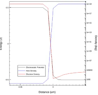
[image:13.595.128.472.301.633.2]There are two ways to determine the depletion width from the simulation. The rst one is to rely on the built in program that will show where it is but because the algo-rithm for nding this is unknown, it is best to nd the depletion layers manually. This is done by either plotting the electric potential or the number of carriers as a function of distance. Both graphs would show a sudden drop or gain at the edge of the depletion layer which indicated where the depletion layer is.
Figure 2.2.2: Carrier concentrations and electric potential for doping concentration 3.
Earlier iterations did not show the expected results but that was resolved by increas-ing the meshincreas-ing size, which in turn increased the duration of the simulations. In the end, these values were very close to each other and support the claim that the simulations can provide valuable insight into the behavior of a semiconductor. It also provided some insight into the workings of the program as the meshing of the structure was detrimental to getting the correct result, which should be kept in mind for future simulations.
2.2.2 Characterization of PN Junction
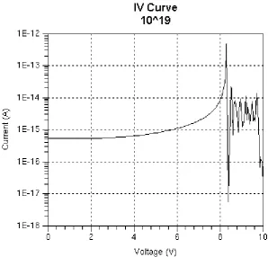
[image:14.595.148.447.328.614.2]The next step was to determine the breakdown voltage of the dierent junctions. This was done exactly the same way as with the BJTs, by sweeping the voltages from 0 to some high value. This time, however, the BreakAtIonIntegral command was omitted to observe the behavior of the simulation past the breakdown point. It resulted in the following graph:
Figure 2.2.3: IV Curve for doping concentration 1019cm−3.
Figure 2.2.3 shows the IV curve obtained for doping concentration 3 and there was a sharp increase in current past the 8V mark. The graph itself was not very clear as to what happens past this point but it gives a rough estimate for the breakdown voltage. The breakdown voltages were ∼55V, ∼19.5V and ∼8V for doping concentrations 1016, 1017
and 1019 respectively. The breakdown voltage increases as the doping level decreases, as
Using these values, the junctions were biased at a point below the breakdown voltage and repeatedly made to avalanche using a on-o pulsing. Just like before, the current through the devices should result in a square wave that is in phase with the input signal up until a repetition rate of ∼1MHz. After that point some pulses are expected to be
[image:15.595.148.446.172.464.2]missing, which is the point of this experiment.
Figure 2.2.4: Transient sweep using a 10MHz on-o signal on the 1017 cm−3 junction.
Figure 2.2.4 shows the current through the emitter junction. Just like the BJT sim-ulations, there was no evidence of a nite repetition rate. The simplicity of the design should have made the dead time interfere at some point, but a 1GHz signal did not evoke any result either. This begs the question as to whether Sentaurus is fully able to simulate the desired avalanching behavior.
2.3 Evaluation of Simulations
Based on the results obtained for both the BJT and the PN-junction, the dead time should have no inuence on the signal transfer if avalanching silicon is used in an opto-coupling device. This, however, contradicts other sources [1][2] and brings into question to what extend Sentaurus is able to simulate an avalanching diode.
This is problematic as the nite repetition rate is heavily reliant on the probability of it not avalanching. This means that Sentaurus is not equipped to simulate the desired switching behavior and so experiments might yield other results.
3 Experiments
[image:16.595.150.449.296.423.2]Due to the limits of Sentaurus's capabilities to simulate avalanching models, some exper-iments were performed in order to nd the dead time because, according to sources [1] [6], it should exist. Based on these sources, V. Agarwal made a few circuit designs meant to test the avalanching behavior of physical diodes and BJTs. There were a variety of circuit designs with a few dierent quenching circuits. The following design is the one that was used throughout this report:
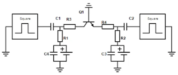
Figure 3.0.1: Circuit design featuring the possibility to actively quench the transistor.
This design features three dierent circuits for each terminal of the transistor. The most simple one is the base, which is grounded. The junction with the lowest breakdown voltage is the emitter-base junction and the base should not inuence this.
The circuit on the emitter side featured a coupling capacitor (C2), a decoupling ca-pacitor (C3), a pulse generator, a DC voltage supply and two resistors (R2 and R4). The DC voltage supply was used to set the biasing point just below the breakdown voltage. The pulse generator would modulate the voltage above the breakdown voltage, making a current ow. The current that owed through R4 should be very low unless the junc-tion is in breakdown. By measuring the voltage over the resistor R4 it should have been possible to identify when the avalanching event.
The collector's circuit was exactly the same as the emitter's circuit but it served a dier-ent purposed. This circuit was made in the case free carriers had to be injected into the BJT. By applying a voltage on the collector junction some carriers would get injected into the PCB which should reduce the dead time of the system, thus increasing the maximum frequency obtainable. The two signal generators would be synchronized in order to inject the carriers at the right time.
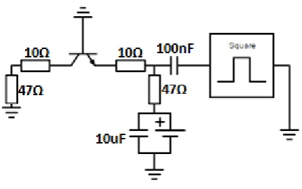
Figure 3.0.2: Simplied version of Figure 3.0.1.
This circuit was then implemented on a PCB design, by V. Agarwal, PCB designed using Agilent Technologies'Advanced Design System (ADS). It is a tool to design PCB which can then be fabricated. The reason a PCB was used is because it would reduce parasitic inuences. SMD components generally produce more stable measurements than their through hole components counterparts. When working with high frequencies, small pieces of wires can act as inductors and create strange impedances. Proper design can create distance between components and thereby reduce the parasitic inductance. V. Agarwal had already performed the experiment using through hole components but he could not nd any missing pulses. He concluded that the parasitic inuences of the through hole components were too high and that SMD components might yield better results.
Figure 3.0.3: ADS design of Figure 3.0.1
[image:17.595.73.529.489.697.2]contacts whereas the white lines indicate the presence of potential PCB components. There are few dierences between this design and the one in Figure 3.0.1, the main dierences being the ability to add a load between the base and a second decoupling capacitor, in case they were needed. The rest is exactly the same.
Figure 3.0.4: Contact denition of SOT23.
With this design, the components were soldered to the PCB and resulted in the circuit shown in Figure 3.0.2.
The rst transistor used with this design is the PMBT2369, an NPN switching tran-sistor which allows a maximum voltage of 5V across the emitter-base junction. [7] This indicates that the breakdown voltage is close to 6 volts. The breakdown voltage was then found using the Hewlett Packard Semiconductor Parameter Analyzer (HP4156B) by performing DC sweep from 0 to 9V and plotting the results on a semi-logarithmic scale:
Figure 3.0.5: Preliminary IV Curve for the DC sweep of PMBT2369.
As stated in the simulations section, the breakdown was dened at the point where dI
[image:18.595.130.467.469.676.2]saturation current also goes down before the breakdown voltage is reached, a phenomenon that is out of place and places doubt on the data collected with the HP4156B. The most important part of this graph was the breakdown voltage which was clearly indicated and was close to the expected value.
3.1 Repeated Avalanching Experiment
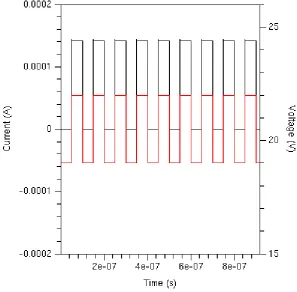
[image:19.595.109.488.358.587.2]This transistor was then soldered onto the PCB board and connected to a variable DC source (Agilent E3631A) and the pattern generator (Anritsu Pulse Pattern Generator MP1763C). A dierential probe (N2803A) with a specialized tip (N2838A) was placed across resistor R4 and attached to an oscilloscope (Agilent Inniium Digital Signal Ana-lyzer). The rst experiment was to keep the biasing voltage at zero to see how the current would change when the transistor is met with an on-o pulse but is not avalanching. The function generator was set to create a 1.2V peak-to-peak square wave which would drive the system. The voltage dierence was measured over a prolonged period of time to collect more pulses within a single set of data, increasing the likelihood that a pulse is missing somewhere indicating the unwanted repetition rate.
Figure 3.1.1: Voltage input vs voltage dierence across resistor R4, no bias.
The rst frequency tested was a 490kHz block wave without biasing voltage. With-out a bias the emitter-base junction should not break down and no current should run through resistor R4. Figure 3.1.1 shows the result of this experiment and it conrms that the current is unaected when the junction is not avalanching.
Figure 3.1.2: Voltage input vs voltage dierence across resistor R4, 6.5V bias.
Figure 3.1.3: : Voltage dierences over resistor R4 with a) no bias and b) 6.5 bias.
when the breakdown voltage is above 10V [8], but 6.5V is somewhere in the between and thus this had to be investigated.
When a junction is highly doped it will create a narrow depletion width and usually have low breakdown voltages. The depletion layer is so thin that electrons are able to tunnel through it, causing a current to ow. It has a negative temperature coecient [9] meaning that an increase in temperature should decrease the breakdown voltage.
Avalanche breakdown only occurs in lowly doped junctions as it requires a larger de-pletion width than a Zener Diode. The mechanism is based on impact ionization, one electron could ionize atoms within the depletion layer, releasing additional electrons. Those released electrons would do the same and this results in the so called Avalanching eect [9].
If the transistor was indeed in Zener breakdown then the temperature coecient should be negative, which can be veried by performing a DC sweep of the emitter-base junction at varying temperatures.
3.2 Characterization of Transistors
Figure 3.2.1: IV curve for the PMBT2369 transistor at varying temperatures.
The rst component to be tested was the PMBT2369 transistor as it is the one used in the previous experiments. Figure 3.2.1 displays the IV characteristics of the transistor at dierent temperatures and it can be seen that the slope shift to the right as tempera-ture increases. This indicates that the breakdown voltage increases with the temperatempera-ture and thus the device had a positive temperature coecient, proving avalanching was the dominant breakdown mechanism.
Figure 3.2.2: IV curve for the BSV52 transistor at varying temperatures.
Figure 3.2.3: IV curve for the BFM520 transistor at varying temperatures.
[image:24.595.82.517.407.679.2]the other two and there was no clear indicator of breakdown. The current through the transistor quickly rose to a value above 0.1A which is above the limit set by the machine. This showed that the BFM520 was unsuitable for testing purposes and the BSV52 was too comparable to the PMBT 2369 so it should not yield dierent results when subjected to a block wave so switching experiment was not repeated.
3.3 Evaluation of Experiments
The experiments did not reveal any data to support the presence of a dead time. After investigating the eect of temperature on the breakdown voltage it was shown that the breakdown mechanism was dominated by avalanching and not Zener breakdown so the eect of tunneling electrons should be minor, if not negligible.
A possible solution was proposed by V. Agarwal, that the leakage current could have been the source of high repetition rates. Most papers talk about situations where the leakage current was in the order of pico-ampere but the transistor had 1 µA saturation current which is a magnitude of 103 larger.
Unlike a SPAD, the dark count rate is an essential variable that makes the AMLED work. A high dark count rate increases the chances of avalanching when the junction is supposed to be in breakdown. Increasing the dark count rate is done by injecting the depletion region with free carriers whenever the junction is not avalanching. According to Y. Kang et al. the current is actually the source of carrier injection, dened by the following equation [10]:
NDM1 =IDM/q (eq.3)
This equation denes the carriers injects NDM1 as a function of the dark current IDM, duty cycle τ and the primary charge of an electron q. When assuming a repetition rate of 50MHz there are about 62,500 carriers being injected into the depletion layer during the time the device is not above the breakdown voltage. Each electron has the ability to start avalanching and the paper gives an equation to calculate that probability:
Pd = 1−exp(−NDM1Pa) (eq.4)
The probability that the dark carriers (Pd) triggers an avalanche is dened as a func-tion of NDM1 and Pa, the probability of starting avalanching by every carrier. Pa in this case is equal to ∼0.5 according to McIntyre [11] for this system, assuming k is equal to
1. This results in a Pd of ∼1, so the carriers injected would avalanche every time the
4 Conclusion
In the end, the nite repetition rate of AMLED was not demonstrated in either sim-ulations or in the experiments. The simsim-ulations are entirely reliant on the ability of Sentaurus to simulate avalanching while the transistor used in the experiments featured a fairly high saturation current, something that could cause signicant carrier injection thus reducing the dead time. Nothing can conclusively be said about the results obtained but there are substantial theories to support the failures of each simulation and experi-ment.
A possible interpretation of the results is that a high leakage current could actually be benecial to the switching behavior of an AMLED. The carrier injection would sub-stantially increase the maximum rate of data transfer than can be attained, but it would also increase the power consumption of the device. The reason for using an AMLED was to reduce the energy consumed in the LED in the o state. It might not be ideal, but it is worth further exploration to compare the energy eciency of these types of transistors with forward LEDs.
For future experiments it is suggested to use a simulation program that takes into account the stochastic nature of avalanching in order to observe the nite repetition rate. The dead time is heavily reliant on the probabilities of avalanching and it cannot be properly simulated. There are currently no known programs that do so.
Bibliography
[1] A. Vilà et al., "Geiger-Mode Avalanche Photodiodes in Standard CMOS Technology" Intech, 2012.
[2] S. Cova et al., "Avalanche photodiodes and quenching circuits for single-photon detection" Applied Optics, pp. 1956-176, 1996.
[3] Synopsys, "Synopsys TCAD," [Online]. Available:
http://www.synopsys.com/tools/tcad/Pages/default.aspx
[4] Ray Hueting, "Semiconductor Devices Explained More". Enschede, Netherlands: University of Twente, 2015.
[5] B.v. Zeghbroeck, Principles of Semiconductor Physics," University of Colorado, 2011. [Online]. Available:
http://ecee.colorado.edu/~bart/book/book/chapter4/ch4_5.htm.
[6] E. Charbon et al., "SPAD-Based Sensors" Springer, 2013.
[7] NXP, "PMBT2369 NPN switching Transitor Datasheet".
[8] R. Dorf, "The Electrical Engineering Handbook," Taylor and Francis.
[9] R. V. Jones, Harvard University, 18 Oct 2001. [Online]. Available:
http://people.seas.harvard.edu/~jones/es154/lectures/lecture_2/ breakdown/breakdown.html. Springer, 2013.
[10] Y. kang et al. "Dark count probability and quantum eciency of avalanche photodiodes for single-photon detection.," Applied Physics Letters, vol. 83, 2003.
5 Appendices
5.1 Appendix A
[image:28.595.72.528.223.488.2]The Sentaurus Workbench consists of various tools, of which one a handful will be used in this report. The rst tool is the Sentaurus Structure Editor (SDE). Using the custom programming language provided for this program, it is possible to make accurate designs on a microscopic scale.
Figure 5.1.1: Sample coding for a BJT junction.
Figure 24 shows a sample code used to create a BJT junction in 2D. The code shown denes various variables that are used to dene geometric shapes. These geometric shapes are given material properties, a function provided by the program. It allows for the clear distinction between material types such as Silicon and Glass. Subsequently, it is also possible to specify the doping concentration in each material, allowing for the choice in dopants as well as the amount of dopants added.
The structure must then be meshed into smaller sections so that the properties of the structure can be determined. A smaller mesh means a higher resolution and will most likely result in the most accurate result, but will also increase the time required to simu-late the structure in any given conditions.
Figure 5.1.2: A design imported to Sentaurus Structure Editor.
The program provides various tools, but it is more time consuming to use the tools provided by the program in order to make an accurate design, thus the structure is usu-ally made in SDE. Figure 25 a design that was made using the coding method, clearly showing the distinction between gold (yellow), Silicon (pink) and glass (brown) areas. It also clearly indicates the dierent contacts, namely the gate (white), emitter (red), base (green) and collector (blue).
Figure 5.1.3: Settings used in the simulations.
Figure 5.1.4: Signal dening code.
5.2 Appendix B
5.3 Appendix C
5.4 Appendix D
Figure 5.4.2: Carrier concentrations and electrostatic potential for Doping 2.
5.5 Appendix E
This simulation was performed to identify the nature of the large peaks in the experi-mental data collection. The circuit in Figure 3.0.2 was replicated and made subject to an on o pulse with a frequency of 50MHz.
[image:35.595.74.523.520.723.2]5.6 Appendix F
[image:37.595.87.515.171.542.2]The gated design was also used to investigate the eect of the gate voltage on the break-down voltage, but as this was not used to simulate switching behavior, it was left out of the paper.
Figure 5.6.1: The IV curves with dierent Gate Voltages.