•
~)YSTEMS
INC.
1B95 N.
Batavia Street
()range, California
92665
7'14-998-6900
TWX: 910-593-1339
~1LS I-DRV11 P
TABLE 0." CONTENTS
Page
INTRODUCTION
PREPARING USER LOGIC
INSTALLATION
Selecting Device Address ... .
Preparing Peripheral Interface Cables ... 3
Illlstalling the Module ... 3
PROCESSOR INTERFACE ... 4
FIXEI) LOGIC/USER LOGIC INTERFACE ... f'
THEORY OF OPERATION ... 6
MAINTENANCE ... ~ . . . 7
DRA \J\(INGS ... 7
Printed in USA
r:J
IJ
fJ
1995 N. Batavia Street Orange, California 92665• 714-998-6900
SYSTEMS INC. TWX:910-593-1339
~Copyright 1977, MDB Systems. Inc. All rights reserved.
LSI-II is a registered trademark of Digital Equipment Corporation.
[image:2.612.75.508.165.403.2]MLSI-DRVIIP
GENERAL-PURPOSE INTERFACE MODULE
I~~TRODUCTION
The MDB MLSI-DR VII P General-Purpose Interface Module acts as an interface to transfer information between the bus of an LSI!II processor, and the user's peripheral device.
TIle MSLI-DR V II P consists of a single quad module containing the following:
a. Fixed logic to interface with the processor, and with the user-built peripheral
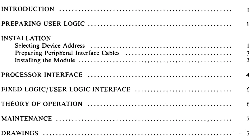
device interface on the module. Fixed logic includes bus receivers and drivers, device address selection and decoding logic, and dual interrupt control logic, (see figure I).
b. Circuit board facilities and wire-wrap posts to accommodate up to fifty-five
14-pin or 16-pin DIP devices. Up to four 20-pin devices; or three 24-pin devices; or two 40-pin devices, along with a smaller number of 20-pin or 24-pin devices; may be installed in place of a number of smaller devices. The user may use these facilities to build logic int.erfacing the fixed logic on the module with the peripheral device.
Control and data points are brought out from the fixed logic to wire-wrap posts to give the user considerable flexibility in using the wire-wrap (user's logic) section of the module. Two-hundred pins are available for interfacing with the peripheral device through
standard ribbon cable connectors.
The quad module fits into any slot in an MDB BPA-84 backplane/card guide ass-embly.
P]REPARING USER LOGIC
Refer to the printed circuit board assembly drawing in this manual for the layout of available DIP device locations. Note that there are 55 device locations for 14-pin or I6-pin DIPs, with pads to accommodate a number of discrete components. Remove etch
connections from DIP pads to ground where they are not appropriate.
Observe good wire dressing practices, especially when speed is important. Decouple the +5V dc line to ground pads (using 0.0 I-microfarad disc capacitors) at at least one point in ealeh DIP column.
Refer to the logic diagram for signals available at wire-wrap pins. Typical user logic may include an output data register, a status register, vector address selection a multiplexer to the IDAT lines, and logic to set or reset interrupt requests.
I~~STALLATION
SELECTING DEVICE ADDRESS
....-W Z « -' Cl. ~ U <: 'E.. w U « LL a:: w ... ~ a:: 0 en en w U 0 a:: Cl. ~
.A IDATOO-15 K
BUS ~
... BDALOO-15 ....
DRIVERS/
C
....
..
~RECEIVERS ODATOO-15
~
L
ODATSTB ADDRESSREGISTER &
~
BBS7L
--"" DECODER
t---.
FUNCTIONr--e
(DECODES) BSYNCL .-. (JUMPERS) DECODER--BRPlYL
--
SYNC [image:4.629.50.560.72.601.2]BDINL .- DATIN
...
p
(DATIN + DATOUT) BDOUTL.-
DATOUT--
-BWTBTL ..- (BYTE)
--
""-(SET ROST 1 & 2)
1
-
VECT 1 BIAKlL .-.P
--
VECLINTERRUPT BIAKOL -.
CONTROL
...
LOGIC VECT 2 BIROL ROST 1 ROST 2
{>o-BINITL
1
(CLEAR ROST 1) (CLEAR ROST 2) INITINITL
Figure I. MOB MLSI-DRVIIP General-Purpose Interface Module, Functional Block Diagram -2-
,..--..
)...
0:-<: a:: S;w
a:: ~ w U « LL a:: w ... ~ Ua
I
0
-'
~ V'
a: w
~
'"'--+12V
GRD
+58
+5V
numbered addresses may be decoded jf additional address inputs are connected to spare address register inputs, and other appropriate wire-wrap jumpers are connected (refer to logic diagram).
To encode a "1", connect the Q output of the stored bit to the AND gate. To encode a "0", connect the
'Q
output to the gate.The Bank 7 Select signal (BBS7L) identifies information from the upper 4K bank (28K to 32K) and is etch-connected to the decoder AND gate.
Wire-wrap terminations give the user almost total freedom in adpressing. The module is furnished etch-connected so that the address decoder is enabled by either DATIN or DATOUT, but the user may change this requirement by cutting the etch connections.
PR.EPARING PERIPHERAL INTERFACE CABLES
The user determines wire-wrap connections at the peripheral device interface. The 200-pin array accommodates standard ribbon cable connectors in any configuration chosen by the user. Where more than one connector is used, be sure to plan pin-outs so that interface signals are grouped together at appropriate connector locations.
INSTAI",LING THE MODULE
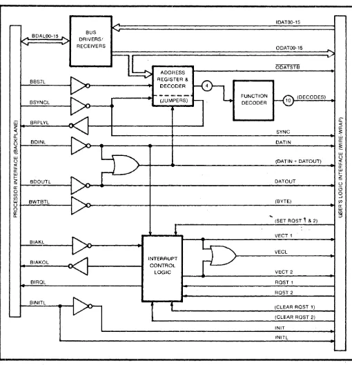
[image:5.611.56.576.353.704.2]After user logic has been completed and appropriately terminated at the cable connector pins, install the module in the slot in the backplane that gives the module the selected priority. The device controller nearest the KD 11 processor board has the highest priority, with decreasing priority at sur.,;essive!y more distant slots (see figure 2) .
... 1 - - - - ROW --....j.~
C B
fOooooooo - - -
-1- - - - -, -
1 :-0 -0 -0 -0 II
I
I
0F - -
---1---
-l-- -- -
~---2
r---
--1---
1 ,
-i--E--:-.-~--!--~-:-t
--- :
1
~--'---1---+---:3-- ~
~-f-+-~-~-~+----.-+---
:
1
: , SRUNL
~
- - - -! ----::---: -
j --
7o
o
r---(--i-~---t---~-:
----
8-I~ -~i-
____ '_--_'
LOW / " PRIORITY
NOTE
If the module does not use DMA and / or Interrupt
operations, the appropriate ~'Acknowledge" lines must be jumpered at connector locations A and C.
Connect the ribbon cables to the device interface connector pins, and to the peripheral device or another MOB module. The module is now ready for check-out and operation.
The MLSI-ORVIIP draws 0.4 ainpere from the +JjV supply bus.
PEtOCESSOR INTERFACE
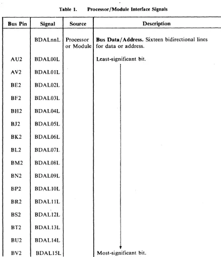
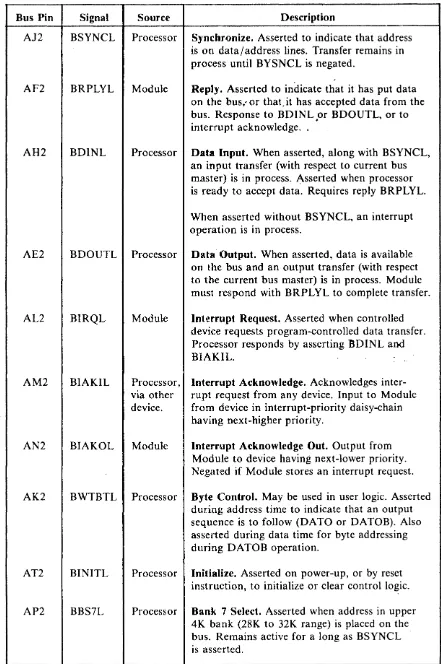
Table I lists and describes signals at the processor/module interface. For additional detailed information, refer to the appropriate manuals for the LSI-II Processor.
Table t. Processor /Module Interface Signals
Bus Pin Signal Source Description
BDALnnL Processor Bus Datal Address. Sixteen bidirectional lines
or Module for data or address.
AU2 BDALOOL Least-significant bit.
AV2 BDALOIL
BE2 BDAL02L
BF2 BDAL03L
BH2 BDAL04L
BJ2 BDAL05L
BK2 BDAL06L
BL2 BDAL07L
BM2 BDAL08L
BN2 BDAL09L
BP2 BDALIOL
BR2 BDALIIL
BS2 BOALI2L
BT2 BDALI3L
BU2 BDAL14L
BV2 BDAL15L Most··significant bit.
[image:6.621.81.519.214.723.2]-4-Table 1. Bus Interface Signals, (cont'd)
E~us Pin Signal Source Description
AJ2 BSYNCL Processor Synchronize. Asserted to indicate that address
is on data / address lines. Transfer remains in process until BYSNCL is negated.
AF2 BRPLYL Module Reply. Asserted to indicate that it has put data
on the bus,~ or that. it has accepted data from the bus. Response to BDINL,.or BDOUTL, or to interrupt acknowledge ..
AH2 BDINL Processor Data Input. When asserted, along with BSYNCL,
an input transfer (with respect to current bus master) is in process. Asserted when processor is ready to accept data. Requires reply BRPLYL.
When asserted without BSYNCL, an interrupt operation is in process.
AE2 BDOUTL Processor Data Output. When asserted, data is available
on the bus and an output transfer (with respect to the current bus master) is in process. Module must respond with BRPLYL to complete transfer.
AL2 BIRQL Module Interrupt Request. Asserted when controlled
device requests program-controlled data transfer. Processor responds by asserting BDINL and
BIAKIL. ..
AM2 BIAKIL Processor, Interrupt Acknowledge. Acknowledges
inter-via other rupt request from any device. Input to Module
device. from device in interrupt-priority daisy-chain
having next-higher priority.
AN2 BIAKOL Module Interrupt Acknowledge Out. Output from
Module to device having next-lower priority. Negated if Module stores an interrupt request.
AK2 BWTBTL Processor Byte Control. May be used in user logic. Asserted
during address tinle to indicate that an output sequence is to follow (DATO or DATOB). Also asserted during data time for byte addressing during DATOB operation.
AT2 BINITL Processor Initialize. Asserted on power-up, or by reset
instruction, to initialize or clear control logic.
AP2 BBS7L Processor Bank 7 Select. Asserted when address in upper
4K bank (28K to 32K range) is placed on the bus. Remains active for a long as BSYNCL is asserted.
[image:7.614.90.531.42.706.2]FIX1ED
LOGIC/USER LOGIC IN''fERFACE
This interface consists of a large number of signals available at wire-wrap pins. Signals include the following (refer to the logic diagram).
a. Data bus driver inputs (lDATOO-IDAT IS).
b. Data bus receiver outputs (ODATOO-ODAT15).
c. Address register
Q
and Q outputs.d. Ten function-select signals obtained by decoding the address.
e" Received control signals from the bus, and signals applied to the bus, as follows:
•
BBS7L•
BSYNCL•
BDINL•
BDOUTL•
BWTBTL•
BINITL•
BRPLYLf. Other interface signals as follows:
• RQSTI and RQST2, plus signals to preset both interrupt requests, and
individlual request clear signals.
• VECT I and VECT2 signals, to be used to gate selected interrupt vector
addresses to the IDAT lines.
• ODATSTB, which may be used to load a user-supplied output register.
• Inputs and outputs of two spare address register flip-flops, and the stored
address bit ODATOO.
• Inputs and outputs of a spare 2-input NAND gate, and a spare 2-input NOR
gate.
THE~()RY
OF OPERATION
(Refer to figure I, and to the logic diagram, Dwg. No. 40345).
The device address on the bus is loaded into the address regis1:er when the processor asserts BSYNCL. When either a BDOUTL or BDINL command is received at the bus, the address decoder is enabled, and address bits 01 and 02 (and, optionally, one or two user-genera1ted bits) are decoded to cause one of up to ten function-select signals to go low.
-6-The module acknowledges receipt of any recognized address, after a short delay, by asserting BRPLYL at the bus. (BRPLYL is also asserted to notify the processor that the interrupt vector address has been placed on the bus.)
The user's logic requests service by asserting either RQST I or RQST2. Either signal is ORed to the BI RQL line to inform the processor that service is required.
The processor responds by asserting BDINL and BIAKIL, loading'the interrupt request flip-flop and then raising the related VEeT I or VECT2 signaI:This signal (in user logic) gates a preset vector address (supplied by user logic) to the IDAT lines, and also causes BRPLYL to be asserted. The processor then enters the addressed subroutine to transfer data to or from the user's peripheral device.
VVhen the operation is completed, the processor drops the BSYNCL line, restoring the fixed logic to its idle state.
Note that the user's logic may set, or clear, an interrupt request at any time.
The term ODATSTB goes low when BRPLYL is asserted in response to a DATIN or DATOUT command.. This signal may be used to load the user's output data register.
l'r1AIN TEN
Al'T teE
If trouble is apparent, first make sure that device and vector addresses are in agreement with system software, and that user's logic sequences are compatible with LSI-II software and hardware sequences.
f\1DB Systems' engineering staff will be pleased to provide technical assistance
by
telephone. Ho',vever, do not ship the user-configured module to MDB Systems for troubleshooting or repair.
I)RAWINGS
('
r.:-
OOAT ISI
I
14.'3 X43 13
I 78
.1'0 L·
~
.42
I
OOAT '28D
1Al15l@
I'
r
1
15
r
I
" L @ )lJJ
13L@
BOAL 12L@
INITl
INIT
IOAT II ·2
I
10 5 8641 .309 X41 14 7A 6
IDAT 08 )(40 II 1.3
)(44 7 10
~9
~ R8+5V I 4 15 12
BOAL ilL
I
10L9L
BOAl8l
~
A52IDAT 07 '1'36 2
1
06 '1'37 5 8641
~TO'
6814 6 06
05 '1'33 X38
IDAT 04
G:ill----..!
I 13 4X33] 05E:ill
7 10 - - ODAT04X32
~9
+-5v 1 4 15 12
8DAL 7l 812
I
6 l §5LC§) BDAL 4L 8HZ
+5V
RQ5T I v2 2
DATIN _ _ _ _ _ _ + __ .3~
~---r---~
~+~~
_ ~ 330
BIAKL@ ... --t--.
RI
680
'1'7
RQ5T 2 Y8
BlAKI
RQ5T1
RQ5T2
1\
OATIN - - - t - - ' - ' i
x8
RPLY~
7432
RQST I 4 IC 6
RQ5fZ
6ND
o ECOUPLI N& CAPACITORS
AS REQUIRED
Ie ... le ... "}
D~
A2 ~+-oI_2z_u_F__
-<I_·o_I1J_F' __ o +5V+ 5v
AAl
IOAr 03 2
I
025 8641 6A
01 X31 14
"
IOATOO X30
7
9
+5V 1 4 15 12
80AL3L 8F2
I
2 L @IL@
BOALOl AUZ
+SV
8837
~4
~~~I-?Y- Sr---7
BBS7L~~ IH C
QDATI2---4~ • !! _ _ _ _ _ _ _ _ _ ..:.:13
4 5A
F--e----~ V6 vECT I
10 _ _ _ _ _ _ _ _ ..:.:12:.f
INITL--_-....:d
09 4
08 12
07 vECL +5V 06 13 5 vEeT 2 9 81AKOL
-:-II ~ B BRPlYL
05
S1 tJ; RPLYI
141
3A 8 0 4
-8641 03
I I 5
12
B BIRQL 02 13
B I
¢ 3 81AKI
.3 6 13 10 6 8837 Y5 NOTE: 1-1O
UNU:SS OTHERWISE SPECIFIED
ALL RESISTOR VALUES ARE lK OHMS AND ARE 1/4W
SPARES
~
21
I 7438 38)3YILl
gg
/I 74021~1~13
L:]wjw POST OCOMPUTER I/O
~
[ill
Iht JIIllfHal Mrlt •• ct."._,."-hrlll"tl'. fh' IS ,r.pfltIJ" ...
"''''rol,"1 I. 1101 STSJlIIS
lilt u~ IS flar •• IN:
t., .... ...
'Isclilul!l t" Ill, 'U",U tlte"
as ~ptCI"tllll llIlhi'IIrf I • • , ....
..
-.
tlOB SYSTEMS. INC. b;"""r.;:-:::::-:::::---r:D=w:::-c; -:::ooo::---r~fIE':-Iv.
""AWN TOM LAMBR05E 0 .40040345 A
COMPo SIDE
REVISIONS
DESCRlPTION APPROVED
The miteflil herein conlalfi~
In-fOlmallgn that IS proPIJeulyand ConfidentIal 10 MOB SYSllMS INC Ind IS nol to be copied 0' Disclosed tor Inv purpose eacepl
is specll,ully lulbOrl1ed '" ";11-ling
ECO NO. 885
...A RELEASE TO PRODUCTION ECO NO. 1174
NOTE: UNLESS OTHERWISE SPECIFIED
1. ASSEMBLE PER QUALIFIED ~~FACTURING STANDARDS
2. SQUARE PADS INDICATE POSITIVE SIDE OF CAPACITORS
AND/OR CATHODE SIDE OF DIODES
3. FOR LIST OF MATERIAL SEE SEPARATE SHEETS
~ DECOUPLING CAPACITORS AS REQUIRED
s. STA."'lP REV. NUMBER \"JHEN APPLICABLE
IN AREA NEXT TO REV. BLOCK
ASSEMBLY O·WG.
N,.TQA
K)lNTIFYING NO.
NOMENCLATURE ".TERIAL
(I:t D!.SCllUP'noH UEClFtCATJQN UNLESS OTHERwISE: SPIC.,IED
Dr,,(frillSI/JNS AAI lit INC""$
tOl.(AAHClS "'''f'
CONTR.ACT NO
PARTS LIST
r:JOB
SYSTEMS, INC.
.IIACn:lO<$ OfCIIJ... AIOQUS
r---r---~ .D-
.IU-DATI IIAflAtAt. 0lIl.1.."
MLSI-DRVIIP
~ __________________ --~C~C~D