SAMPLE-AND-HOLD INPUTS, DUAL ANALOG OUTPUTS,
AND 16-bit DIGITAL
1/0
FEATURES
ANALOG INPUTS• EIGHT SAMPLE-AND-HOLD SCANNING ANALOG
INPUT CHANNELS
• CONTINUOUS OR SYNCHRONOUS SEQUENCING
• MUL TIBOARD OR INDEPENDENT SYNCHRONIZING
• 12-bit AID CONVERTER, WITH RANGES OF
o
TO 10 V, ±5 V, AND ±10 V • INTERRUPTS• PGA PROVIDES PROGRAM CONTROLLED GAINS
OF X1 , X2, X4, X8, AND X16 ANALOG OUTPUTS
• 125 kHz MAXIMUM SCAN RATE (GAIN
=
x1)• DUAL 128 Kbyte DATA BUFFERS
DIGITAL 1/0
• DUAL 8-bit TTL I/O PORTS, PROGRAM
CONTROLLED AS INPUTS OR OUTPUTS
GENERAL
• DUAL-PORTED DATA BUFFERS APPEAR
AS MEMORY TO VME HOST
• DUAL DEGLITCHED 12-bit SCANNING ANALOG
OUTPUTS
• OUTPUT RANGES OF 0 TO + 10 V, ±5 V, AND ±10 V
• 10 rnA LOAD CAPACITY
• 125 kHz MAXIMUM UPDATE RATE
• DUAL 128 Kbyte DATA BUFFERS
• ON-LINE OR OFF-LINE OPERATION UNDER PROGRAM
CONTROL
VME MICROSYSTEMS INTERNATIONAL CORPORATION 12090 South Memorial Parkway
Huntsville, Alabama 35803-3308
(205) 880-0444 FAX No.: (205) 882-0859
1-800-322-3616
Revised 29 May 1992
Specifications subject to change without notice. Copyright © July 1989 by VMIC
VMIVME-3114
ANALOG INPUT/OUTPUT BOARD
INTRODUCTION
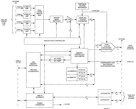
The VMIVME-3114 is a 12-bit input/output board which provides eight analog inputs, two analog outputs, and dual 8-bit bi-directional digital input/output ports for VMEbus system applications. Dual ported data memory, on-board timers, and a program controlled bus interrupter enabte the VMIVME-3114 Board to support extensive analog input and output traffic with minimum involvement of the host processor.
FUNCTIONAL CHARACTERISTICS
GENERAL DESCRIPTIONS:
SEQUENCE INITIATION:
DIGITAL I/O PORTS:
COMPLIANCE:
SPECIFICATIONS
Sample-and-hold input amplifiers provide "snapshot" simultaneous sampling of all analog inputs at aggregate sample rates up to 125 kHz, and virtually eliminate time skewing between input channels. The VMIVME-3114 supports both
independent and multiboard synchronization. Dual analog outputs enable the board to "close the loop" in system servo applications. The VMIVME-3114 functional block diagram is shown in Figure 1.
Analog Input data is stored sequentially in dual 64 Kword buffer memories. The host controls which of the two buffers resides in VME memory through a single toggle bit in the Control and Status Register (CSR). The host can direct the board to generate an interrupt when a scanning sequence is completed.
Dual analog output channels are deglitched to ensure minimum output noise, and can drive 10 mA loads over the maximum output range of ±1 0 V. Dual 64 Kword buffer memories for the analog outputs are identical to the analog input buffers, and provide the same control features. On-line or off-line (disconnected) operation is program controlled.
Analog inputs and outputs can be programmed to scan continously, or to stop at the end of a buffer. Scan rates can be provided by on-board or external clocks, or by software single-stepping. Up to seven slave boards can synchronize to a master VMIVME-3114. Input and output scan rates are independent.
The buffer memories appear as 128 Kbytes of VMEbus memory. To simplify automatic system configuring, the buffers are disabled during power-up and reset operations. To support multiple VMIVME-3114 Boards without requiring additional memory space, the buffers can be removed from VME memory entirely through a control bit in the I/O space CSR. The buffers are program locatable on any 4 0000 byte (HEX) boundary in the VMEbus memory space. Block Mode D16 data transfers (BL T) are supported.
The input and output scans have separate resets. These can be used to start scans at specific moments.
16-bit parallel digital input and output capability is provided by dual 8-bit TTL data ports. Each port can be program configured as either an input or output port, and is accessible in the short I/O space in which the control registers for the boards are located.
A32/A24/A16:D16/D08 (EO) DTB Slave: BLT D16 Slave. Interrupters (2): 1(1) to 1(7) ROAK.
ANALOG INPUTS 8 SE
4 DI
/ ' - - - : - ; ---'
I CHAN!
I
S~~~Hf-4-CHAN ANALOG MUX
/ ~--~--~
CHAN 4
I
SANDHL
/ - . AMPI
~I
I
/ CHAN? J SA~DH
L.
/ -I AMP
I
~'---.---'ANALOG MODE SWITCHES
/
i
~
SAMPLING12-bitAiD CONVERTER
)'3
I
ANALOG INPUT CONTROLLER
I
VMEbus
P1, P2 VME MEMORY INTERFACE
AND BUS INTERRUPTER
'With sign extension.
.1 AID TIMER 1 1 DIATIMER 1
MEMORY CONTROLLER AND ARBITER +10.00VDC ~ I---L...- DUAL
I /12 - 12-bit D/A
DEGLITCHED
1 - - - + - - - 1 1 .. 1 CONVERTERS
1/0 CONN P3
/
/ I
"2 I
/ /
/ / (INDEPENDENT AND "' 4
MUL TIBOARD / SYNCHRONIZATION)
/
S3114/F-l
Figure 1. VMIVME-3114 Analog lID Board Block Diagram (a-Channel, 12-bits, Sample-and-Hold Analog Inputs)
DUAL ANALOG OUTPUTS SYNC I/O DUAL 8-bit DIGITAL
1/0 PORT
~
.J:>.
6
[image:3.795.104.677.74.531.2]I/O ADDRESSING:
MEMORY ADDRESSING:
I/O ADDRESS SELECTION:
ACCESS PRIVILEGE:
VME INTERRUPT:
BOARD IDENTIFICATION:
INITIAL OPERATION:
Addressable as 16 contiguous 16-bit registers, located on any 16-word boundary within the short supervisory or short nonprivileged I/O space.
The input and output buffers appear as conventional memory to the VME host. Total memory space occupied by the board is 256 Kbytes, and can be program located on any 4 0000 byte (HEX) boundary in the VMEbus memory space. The VMIVME-3114 buffers can be removed (masked) from VME memory, by a CSR control bit, thereby permitting multiple boards to occupy the same memory space.
Board address in the short I/O space is selected by on-board field selectable jumpers. Operation is supported in any slot except slot 1.
Address modifiers are decoded to support either supervisory or nonprivileged access, or both accesses. Jumpers are provided to support this feature, and is factory configured for either access. Decoded modifier codes include 09, OA, OB, 00, OE, OF, 20, 29, 39, 3A, 3B, 3D, 3E, and 3F.
The VMIVME-3114 can be programmed to generate separate interrupts for input and output end-of-buffer conditions. The interrupt levels ard response vectors (status/IDs) are programmable.
The Board Identification Register contains the VMIVME-3114 identification code. The following default conditions are established at RESET:
- Continuous operation. - Minimum block size. - Analog Input Gain = x1. - Maximum conversion rate. - Analog outputs disconnected. - Digital ports configured as inputs.
ELECTRICAL SPECIFICATIONS (TYPICAL @ 25°C)
ANALOG INPUTS
NUMBER OF INPUTS CHANNELS:
RESOLUTION:
VOLTAGE RANGES:
VOLTAGE GAIN:
INPUT IMPEDANCE:
INPUT SAMPLING:
INTERCHANNEL PHASE SKEW:
CONVERSION RATE:
PER CHANNEL CONVERSION RATE:
ACQUISITION TlME:
SETTLING TIME:
CONVERSION CYCLE: (Setting plus Conversion)
Eight single-ended or four differential channels. 12 bits.
o to + 10 V, ±5 V, ±10 V; jumper-selectable. Program-selectable as x1 , x2, x4, xB, x16. 1 MQ minimum.
Simultaneous sampling of all analog inputs. Less than 0.10 at 5 kHz.
977 Hz to 125 kHz (aggregate) in 7 equal ratios of 2:1 (internally generated). Up to 125 kHz by external or software sync.
Up to 31,250 Hz for four channels. Up to 15,625 Hz for eight channels. Same as conversion cycle, see Note 2. 3.5 Ilsec maximum, to 0.02 percent; Gain = x1.
CROSSTALK REJECTION: 72 dB at 1 kHz.
INPUT OFFSET: ±2.0 mV maximum.
INPUT BIAS CURRENT: ±200 nA.
INPUT PROTECTION: ±25 V, sustained. (1) KSPS = Thousand samples per second.
(2) Inputs are "pipelined" sample acquisition occurs while the previously acquired channel sample is digitized.
ANALOG OUTPUTS
NUMBER OF OUTPUT CHANNELS:
RESOLUTION:
MONOTONICITY:
OUTPUT MODES:
VOLTAGE RANGES:
OUTPUT IMPEDANCE:
SCAN RATE:
DATA CODING:
SETTLING TIME:
LINEARITY ERROR:
OUTPUT OFFSET:
LOAD CURRENT:
LOAD CAPACITANCE:
OUTPUT PROTECTION:
OFF-LINE OUTPUT LEAKAGE:
BUFFER MEMORIES
ANALOG INPUT BUFFER SIZE:
ANALOG OUTPUT BUFFER SIZE:
VMEbus ACCESS:
VMEbus ACCESS LOCATION:
CONTROL:
OPERATING MODES:
DIGITAL I/O PORTS
ORGANIZATION:
Two independent, deglitched analog outputs. 12 bits.
12 bits over operating temperature range.
On-line (output connected to I/O connector) or off-line (outputs disconnected from 110 connector).
o to + 10 V, ±5 V, ±10 V, jumper-selectable. Less than 0.5 Q.
3.S Hz to 125 kHz in 15 equal ratios of 2:1 (interna"y generated). Up to 125 kHz external sync or software sync.
Two's complement, binary or offset binary. 20 I..ls maximum to 0.02 percent.
±0.03 percent maximum. ± 5 mV maximum.
± 10 mA maximum, over full output range of ±1 0 V. 3,000 pF, no oscillation.
Continuous short to ground; ±25 V for one second. 50 nA.
Two words to 64 Kwords, in 15 equal ratios of 2:1. Two words to 64 Kwords, in 15 equal ratios of 2:1. OS or 016; conventional or block mode transfers.
Program locatable on any 4 0000 byte (HEX) boundary from 00000000 to FFFCOOOO (HEX).
Disabled at power-up and during reset operations. Enabled or disabled through the short I/O space CSA.
Continuous or single block.
Dual S-bit bi-directional ports.
LOGIC LEVELS: Standard TTL levels with no inversions.
VMEbus ACCESS: Single 16-bit register is short I/O space, 08 or 016 access.
CONTROL: Each port is program-controlled as either an input port or an output port.
PHYSICAL AND ENVIRONMENTAL SPECIFICATIONS
TEMPERATURE:
RELATIVE HUMIDITY:
ALTITUDE:
COOLING:
Operating: Storage:
o to +55 cC. 40 to +85 cC. 10 to 80 percent noncondensing. Operation to 10,000 feet. Forced air convection.
DIMENSIONS: Standard VME double height board, 160 x 233.35 mm.
INPUT/OUTPUT CONNECTORS: Refer to Ordering Information.
POWER REQUIREMENTS 5.1 A (typical) @ +5.0 VDC +0.25/-0.125 VDC . 7.3 A (maximum).
from:
REFERENCE MATERIAL LIST
For a detailed explanation of the VMEbus and its characteristics, the publication "The VMEbus Specification" is available
VITA
VMEbus International Trade Association 10229 N. Scottsdale Road Scottsdale, AZ 85253 (602) 951-8866
The following Application and Configuration Guides are available from VMIC to assist the user in the selection, specification, and implementation of systems based on VMIC products.
Digital Input Board Application Guide Change-of-State Board Application Guide
Digital I/O (with Built-in-Test) Product Line Description
Synchro/Resolver (Built-in-Test) Subsystem Configuration Guide Analog I/O Products (with Built-in-Test) Configuration Guide Connector and I/O Cable Application Guide
DOCUMENT NO.
VMIVME-3114 ANALOG INPUT/OUTPUT BOARD
ORDERING INFORMATION
VMIVME-3114 - ABC
L
O=nolused0= not used
0= not used
MODEL NO.
1/0 CONNECTOR DATA (*)
P2 P3 P4 P5
TYPICAL CONNECTING COMPONENT (PANDUIT) (AMP) (AMP) (AMP)
COMPATIBLE MATING CONNECTOR
(Insulation Displacement) 120-964-435E 747945-5 747943-5 747949-5
STRAIN RELIEF (FERRULE) 1 00-000-032 1-747579-0 747579-8 747580-8
101-096-033A 747841-3 747840-3 747843-3
P.C. BOARD HEADER CONNECTOR (96-pin DIN) (15-pin PLUG) (9-pin PLUG) (37-pin PLUG)
*P3, P4, and P5 are standard D-Subminiature connectors.
12-bit ANALOG INPUT/OUTPUT BOARD
8 INPUT CHANNELS, 125 kHz
WITH SAMPLE-AND-HOLD INPUTS
AND DYNAMIC ANALOG OUTPUTS
INSTRUCTION MANUAL
DOCUMENT NO. 500-003114-000 A
4 February 1993
VME MICROSYSTEMS INTERNATIONAL CORPORATION 12090 SOUTH MEMORIAL PARKWAY
HUNTSVILLE, AL 35803-3308 (205) 880-0444
The information in this document has been carefully checked and is believed to be entirely reliable. While all reasonable efforts to ensure accuracy have been taken in the preparation of this manual, VMIC assumes no responsibility resulting from omissions or errors in this manual, or from the use of information contained herein.
VMIC reserves the right to make any changes, without notice, to this or any of VMIC's products to improve reliability, performance, function, or design.
VMIC does not assume any liability arising out of the application or use of any product or circuit described herein; nor does VMIC convey any license under its patent rights or the rights of others.
VME Microsystems International Corporation
All Rights Reserved
This document shall not be duplicated, nor its contents used for any purpose, unless granted express written permission from VMIC.
Copyright (01987 by
VMIC.
REVISIONLETTER DATE PAGES INVOLVED
A 02103/93 Release
CHANGE NUMBER
THE FOLLOWING GENERAL SAFETY PRECAUTIONS MUST BE OBSERVED DURING ALL PHASES OF THIS OPERATION, SERVICE, AND REPAIR OF THIS PRODUCT. FAILURE TO COMPLY WITH THESE PRECAUTIONS OR WITH SPECIFIC WARNINGS ELSEWHERE IN THIS MANUAL VIOLATES SAFETY STANDARDS OF DESIGN, MANUFACTURE, AND INTENDED USE OF THE PRODUCT. VME MICRO SYSTEMS INTERNATIONAL CORPORATION ASSUMES NO LIABILITY FOR THE CUSTOMER'S FAILURE TO COMPLY WITH THESE REQUIREMENTS.
GROUND THE SYSTEM
To minimize shock hazard, the chassis and system cabinet must be connected to an electrical ground. A three-conductor AC power cable should be used. The power cable must either be plugged into an approved three-contact electrical outlet or used with a three-contact to two-contact adapter with the grounding wire (green) firmly connected to an electrical ground (safety ground) at the power outlet.
DO NOT OPERATE IN AN EXPLOSIVE ATMOSPHERE
Do not operate the system in the presence of flammable gases or fumes. Operation of any electrical system in such an environment constitutes a definite safety hazard.
KEEP AWAY FROM LIVE CIRCUITS
Operating personnel must not remove product covers. Component replacement and internal adjustments must be made by qualified maintenance personnel. Do not
replace components with power cable connected. Under certain conditions,
dangerous voltages may exist even with the power cable removed. To avoid injuries, always disconnect power and discharge circuits before touching them.
DO NOT SERVICE OR ADJUST ALONE
Do not attempt internal service or adjustment unless another person, capable of rendering first aid and resuscitation, is present.
DO NOT SUBSTITUTE PARTS OR MODIFY SYSTEM
Because of the danger of introducing additional hazards, do not install substitute parts or perform any unauthorized modification to the product. Return the product to VME Microsystems International Corporation for service and repair to ensure that safety features are maintained.
DANGEROUS PROCEDURE WARNINGS
Warnings, such as the example below, precede only potentially dangerous procedures throughout this manual. Instructions contained in the warnings must be followed.
WARNING
I
DANGEROUS VOLTAGES, CAPABLE OF CAUSING DEATH, ARE PRESENT IN THIS SYSTEM. USE EXTREME CAUTION WHEN HANDLING, TESTING, AND ADJUSTING.
GENERAL DEFINITIONS OF SAFETY SYMBOLS USED IN THIS MANUAL
Instruction manual symbol: the product is marked with this symbol when it is necessary for the user to refer to the instruction manual in order to protect against damage to the system.
Indicates dangerous voltage (terminals fed from the interior by voltage exceeding 1000 volts are so marked).
OR @_,protectiveconductorterminaI.FOrprotection against electrical shock in case of a fault. Used with field wiring terminals to indicate the terminal which must be connected to ground before operating equipment.
m
OR.J..
WARNING
I
** *** ***** * *** * ** * CAUTION *
* *************** *
Low-noise or noiseless, clean ground (earth) terminal. Used for a signal common, as well as providing protection against electrical shock in case of a fault. Before operating the equipment, terminal marked with this symbol must be connected to ground in the manner described in the installation (operation) manual.
Frame or chassis terminal. A connection to the frame (chassis) of the equipment which normally includes all exposed metal structures.
Alternating current (power line).
Direct current (power line).
Alternating or direct current (power line).
The WARNING sign denotes a hazard. It calls attention to a procedure, a practice, a condition, or the like, which, if not correctly performed or adhered to, could result in injury or death to personnel.
VMIVME-3114
12-bit ANALOG INPUT/OUTPUT BOARD 8 INPUT CHANNELS,
125 kHz WITH SAMPLE-AND-HOLD INPUTS AND DYNAMIC
ANALOG OUTPUTS
TABLE OF CONTENTS
SECTION 1. GENERAL DESCRIPTION
1.1 INTRODUCTION ... 1-1
1.1.1 VMIVME-3114 High Rate 12-bit Analog Inputs ... 1-1
1.1.2 VMIVME-3114 Dual 12-bit Analog Outputs ... 1-1
1.1.3 VMIVME-3114 Digital Input/Output Ports ... 1-3
1 .2 FUNCTIONAL DESCRiPTION ... 1-3
1.3 REFERENCE MATERIAL ... 1-5
SECTION 2. PHYSICAL DESCRIPTION AND SPECIFICATIONS
SECTION 3. THEORY OF OPERATION
3.1 INTRODUCTION ... ~ ... 3-1
3.2 INTERNAL FUNCTIONAL ORGANIZATION ... 3-1
3.3 SHORT 1/0 CONTROL INTERFACE ... 3-2
3.3.1 ReadIWrite Operations ... 3-2
3.3.2 Bus Interrupter ... 3-2
3.4 STANDARD AND EXTENDED MEMORY DATA TRANSFERS ... 3-2
3.5 DATA BUFFERS ...•... 3-4
3.5.1 Input Buffers ... 3-4
3.5.2 Output Buffers ...•... 3-4
3.5.3 Buffer Arbitration and Refresh ... 3-4
3.6 ANALOG INPUT SYNCHRONIZATION ... 3-6
3.6.1 Sync Mode ... 3-6
3.6.2 Asynchronous Operation ... 3-6
3.6.3 Synchronous Operation ... 3-6
3.7 ANALOG INPUT PROCESSING ... 3-6
3.7.1 Sampling, Multiplexing, and Digitizing ... 3-6
3.7.2 Data Retrieval ... ~ ... 3-8
3.7.3 Loopback Testing ... 3-8
3.8 ANALOG OUTPUTS ... 3-8
3.8.1 Digital-ta-Analog Converters ... 3-8
3.8.2 Analog Outputs Synchronization ... 3-8
3.9 DIGITAL
VO
PORTS ... 3-93.1 0 POWER CONVERTER ... 3-9
TABLE OF CONTENTS (Continued)
SECTION 4. PROGRAMMING
4.1 4.2 4.3 4.4 4.5 4.5.1 4.5.2 4.5.3 4.5.4 4.5.5 4.5.6 4.6 4.6.1 4.6.2 4.6.3 4.7 4.7.1 4.7.2 4.7.3 4.8 4.8.1 4.8.2 4.8.3 4.8.4 4.9 4.9.1 4.9.2 4.10 4.11 4.11.1 4.11.2 4.12 4.12.1 4.12.2 4.12.3 4.12.4 4.12.5
INTRODUCTION TO CONTROLLING THE VMIVME-3114
TABLE OF CONTENTS (Continued)
SECTION 5. CONFIGURATION AND INSTALLATION
5.1 UNPACKING PROCEDURE ... 5-1
5.2 PHYSICAL INSTALLA TION ... 5-1
5.3 BEFORE APPLYING POWER: CHECKLIST ... 5-1
5.4 OPERATIONAL CONFIGURATION ... 5-2
5.4.1 Factory Installed Jumpers ... 5-2
5.4.2 Board Location in Short 1/0 Space ... 5-5
5.4.3 Data Buffer Location ... 5-7
5.4.4 Data Coding ... 5-7
5.4.5 Analog Input Configuration ... 5-7
5.4.6 Analog Input Range Selection ... 5-7
5.4.7 Analog Output Range Selection ... 5-7
5.5 CALIBRATION ... 5-9
5.5.1 Equipment Required ... 5-9
5.5.2 Analog Outputs Calibration Procedure ... 5-9
5.5.3 Analog Inputs Calibration Procedure ... 5-12
5.6 CONNECTOR DESCRIPTIONS ... 5-12
SECTION 6. MAINTENANCE AND WARRANTY
6.1 MAINTENANCE ... 6-1
6.2 MAINTENANCE PRINTS ... 6-1
6.3 WARRANTY ... 6-1
6.4 OUT-OF-WARRANTY REPAIR POLICY ... 6-2
6.4.1 Repair Category ... 6-3
6.4.2 Repair Pricing ... 6-3
6.4.3 Payment ... 6-3
6.4.4 Shipping Charges ... 6-4
6.4.5 Shipping Instructions ... 6-4
6.4.6 Warranty on Repairs ... 6-4
6.4.7 Exclusions ... 6-4
Figure
1.1-1 1.2-1 3.3-1 3.5.1-1 3.7.1-1
LIST OF FIGURES
faWt
VMIVME-3114 Analog Input/Output Board ... 1-2 Functional Block Diagram ... 1-4 VMEbus Interface Logic ... 3-3 VMIVME-3114 Memory Buffers ... 3-5 Analog Input Processing (Single-Ended) ... 3-7
Figure
3.9-1 4.1-1 4.5.5-1 4.12.1-1 4.12.1-2 5.4-1 5.5-1 5.6-1 5.6-2
Table
4.1-1 4.4-1
4.5.4-1 4.6.2-1 4.6.3-1 4.8.1-1 4.8.3-1 4.9-1 4.9.1-1 5.4-1 5.4.2-1 5.4.6-1 5.6-1" 5.6-2 5.6-3
TABLE OF CONTENTS (Concluded)
LIST OF FIGURES (Concluded)
~
Digital 110 Ports and Analog Outputs ... 3-10 VMIVME-3114 Memory Buffers ... 4-3 ADC Data Format and Coding ... 4-9 Program Example - 3114 Header File ... 4-19 Program Example - C Source Code ... 4-22 VMIVME-3114 Jumper Option Locations ... 5-3 VMIVME-3114 Test Points and Adjustments ... 5-1 0 P1/P2 Connector Pin - Configurations ... 5-13 P3, P4, and P5 Connector Pin Configurations ... 5-14
LIST OF TABLES
~
VMIVME-3114 Short 1/0 Register Map ... 4-2
VMIVME-3114 Board Control and Status Register (CSR)
Functions ... 4-5 Input Control Register (ICR) ... 4-8 Analog Input Synchronization Modes ... 4-11 Scan Status Register (SSR) ... 4-11 Output Control Register (OCR) ... 4-14 Analog Output Synchronization Modes ... 4-1 4 Interrupt Registers Organization ... 4-16 Interrupt Control Register Functions ... 4-17 Programmable Jumper Functions ... 5-4 Typical Board Address Selection ... 5-6 Analog Input and Output Range Selection ... 5-8 P2 User-Pin and P4 Signal Assignments ... 5-16 Analog Inputs Signal Assignments ... 5-16 P5 Signal Pin ASSignments ... 5-17
APPENDIX
SECTION
1
GENERAL DESCRIPTION
1.1 INTRODUCTION
The VMIVME-3114 (Figure 1.1-1) is a member of VMIC's extensive family of analog input/output board products for the VMEbus. The board provides automatic scanning of both analog input and output functions, and represents a complete analog input/output subsystem. Digital ports also are included for controlling and monitoring TTL interfaces. Simultaneous sampling of eight analog input channels provides the minimum skew characteristics required in modern sampled data systems. Two dynamic analog output channels are available for the generation of arbitrary analog stimulus functions.
A summary of principal features illustrates the performance and flexibility offered by the VMIVME-3114 Board:
1.1.1 VMIVME-3114 High Rate 12-bit Analog Inputs
a. Simultaneous sampling of eight single-ended or four differential
analog inputs
b. Aggregate conversion rates to 125 kSPS (thousand samples per
second)
c. Input ranges of 0 to +5 V, 0 to +10 V, ±2.5 V, ±5 V, and ±10 V
d. Program controlled gains of x1 , x2, x4, x8, and x16
e. Dual 64-Kword data buffers
f. High-speed 3 J.1sec 12-bit Analog-to-Digital Converter (ADC)
g. Program controlled input block size and scan rate
h. Continuous, burst, single-step, and multiboard synchronization
i. Bus interrupter for block-full indication
j. Loopback self-test
1.1.2 VMIVME-3114 Dual 12-bit Analog Outputs
a. Output ranges of 0 to +10 V, 0 to +5 V, ±2.5, ±5 V, and ±10 V
b. Dual 64-Kword data buffers
c. Dual, deglitched 12-bit Digital-to-Analog Converter
d. Program controlled output block size
e. Continuous, burst, single-step, and multiboard synchronization
f. 10 rnA output load capacity over full output range
g. On-line or off-line operation under program control
h. Bus interrupter for end-block indication
i. Scan rates to 125 kSPS for each channel
(Photograph of VMIVME-3114)
M31141F1.1-1
1.1.3 VMIVME-3114 Digital Input/Outpyt Ports
a. Dual independent 8-bit TIL input/output ports
b. Individually program controlled as input or output ports
1.2 FUNCTIONAL DESCRIPTION
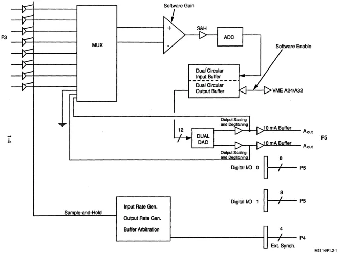
The VMIVME-3114 (Figure 1.2-1) is a high throughput 12-bit Analog Input/Output (AIO) Board which provides eight sample-and-hold analog inputs, two dynamic analog outputs, and dual 8-bit bi-directional digital input/output ports for VMEbus system applications. Dual ported data memory, on-board rate generators, and a program controlled bus interrupter enable the board to support extensive analog input and output traffic, with minimum involvement of the host processor.
Analog input data is stored sequentially in two 64-Kword buffer memories. A bit in the Control and Status Register (CSR) selects one of the buffers for access as VME memory. VME controlled registers determine the active block size of the buffers, and the input scanning rate. The host can direct the board to generate an interrupt when an input block is filled. Input gain, active buffer size, and preset scan rate are controlled by the Input Control Register (ICR).
Analog inputs can be scanned at a preset rate or synchronized to an external sig nal.
Analog inputs can be sequenced either continuously, single block synchronously, or multiboard synchronously. In the continuous mode, input scanning proceeds continuously unless stopped by the host processor. The VMIVME-3114 fills one input buffer while the host reads the other. In the single block synchronous mode, a preselected input block is filled and the input sequence halts. Multiboard synchronization can be applied in either the continuous or single block modes, with a designated master controlling other VMIVME-3114 Boards.
To simplify automatic system configuring, VME access to the input and output buffers is disabled after power-up and reset operations. VME-to-buffer access is enabled by a bit in the CSR. This bit makes it possible for several VMIVME-3114 Boards to share a buffer address, thus conserving memory space. The buffer is jumper-locatable on any 20000 (HEX) word boundary in the VMEbus memory space.
Dual dynamic analog output channels can drive 10 mA loads over the maximum output range of ±10 V. On-line operation (outputs connected to I/O connector) or off-line operation (disconnected) is program controlled. Each of the two analog output channels is driven from a dedicated 64-Kword data buffer. Control and synchronization of the analog output buffers is essentially identical to that of the analog input buffers, but is independent of analog input activity.
P3
MUX
Sam le-and-Hold
Input Rate Gen. Output Rate Gen.
ADC
Software Enable
Dual 'Circular _I~~t..e~ff.:r:. __ _
12
Dual Circular Output Buffer
DUAL DAC
VME A24/A32
10 mA Buffer
A out
10 mA Buffer
A out
Digital
va
0~
P5DlgitalltO 1
~
P5P5
CJ1
[image:20.799.43.714.38.535.2]1.3 REFERENCE MATERIAL
For a detailed explanation of the VMEbus and its characteristics, the publication "The VMEbus Specification" is available from:
VITA
VMEbus International Trade Association 10229 N. Scottsdale Road
Scottsdale, AZ 85253 (602) 951-8866
The following Application and Configuration Guides are available from VMIC to assist in the selection, specification, and implementation of systems based upon VMIC's products:
TITLE
Digital Input Board Application Guide Change-of-State Application Guide Digital I/O (with Built-in-Test) Product Line Description
Synchro/Resolver (Built-in-Test) Subsystem Configuration Guide
Analog I/O Product (with Built-in-Test) Configuration Guide
Connector and I/O Cable Application Guide
1-5
DOCUMENT NO.
825-000000-000 825-000000-002 825-000000-003
825-000000-004
825-000000-005
SECTION 2
PHYSICAL DESCRIPTION AND SPECIFICATIONS
3.1 INTRODUCTION
SECTION 3
THEORY OF OPERATION
The VMIVME-3114 Board uses a high-speed Analog-to-Digital Converter (ADC) and pipelined Sample-and-Hold Amplifiers (S&H), to achieve high rate sampling and 12-bit digitizing of eight single-ended or four differential analog inputs. All inputs are sampled simultaneously to eliminate time skewing, and their digitized values are stored sequentially in Dynamic RAM (DRAM) data buffers. Input scanning can be operated asynchronously, or can be synchronized either to an external signal or to another VMIVME-3114 Board.
Dual Digital-to-Analog Converters (DACs) convert 12-bit digital values from scanned data buffers into two dynamic analog output channels. The data buffers can be scanned automatically, or can be single-stepped or synchronized to either an external sync signal or to another VMIVME-3114 Board. A self-test multiplexer permits the analog outputs to be routed to the analog input multiplexers for loopback self-testing.
In addition to the analog input and output functions, the board provides two
independent 8-bit digital 110 ports.
3.2 INTERNAL FUNCTIONAL ORGANIZATION
The VMIVME-3114 Board contains the following hardware functions:
a. VMEbus interface and bus interrupter b. Input and output data buffers
c. Analog input sampling, multiplexing, and digitizing d. Analog input synchronization
e. Analog output DACs, deglitching, switching, and protection
1. Analog output synchronization
g. Digital 110 ports h. Power converters
The Control and Status Register (CSR) establishes the operational mode of the board. The Input Control Register (ICR) and Output Control Register (OCR) establish the sizes of the input and output memory blocks, and control the input and output scan rates. The Scan Status Register (SSR) monitors the status of input and output scanning operations.
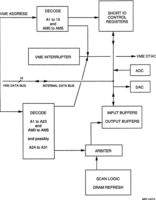
3.3 SHORT 1/0 CONTROL INTERFACE
Control of data transfers between the board and the VMEbus is illustrated in Figure 3.3-1. Data transfers are supported anywhere in the VMEbus short I/O
space. Address modifiers AMO through AM5 are decoded to support both
supervisory and nonprivileged access. The registers which are used to control and monitor the board occupy a 16-word block which can be located on any 16-word boundary within the VMEbus short I/O space.
3.3.1 ReadlWrite Operations
VMEbus data transfer requests are ignored unless the board-selection comparator detects a match between the selection jumpers and the address and address modifier lines from the backplane. When a valid match is detected, the board prepares for a data transfer, and asserts the open collector DTACK interface signal (LOW). DTACK returns to the negated (HIGH) state when the transfer has been completed.
Data Bus lines DOO through D15 are bi-directional and move data to or from the board through a 16-bit data transceiver in response to control signals from the I/O control timer. The data transceiver serves as a buffer for the internal data bus which interconnects all short I/O devices on the board. Address lines A05 through A 15 map the communication registers onto an 16-word boundary within the VME short I/O space (Section 4). Data transfer control signals from the VMEbus determine whether data is moved to the board (Write) or from the board (Read). Both D8 and D16 transfers are supported.
3.3.2 Bus Interrupter
To eliminate the processing overhead usually associated with process polling, access to the VME interrupt structure is provided through a bus interrupter. If the interrupt is enabled, an interrupt is generated in response to an INTERRUPT REQUEST signal, which indicates the end of an input or output buffer. The interrupt function is implemented with a Bus Interrupter Module (BIM). Control Registers for the interrupter occupy four word locations in the short I/O space. Details of interrupter capabilities are described in Section 4.
3.4 STANDARD AND EXTENDED MEMORY DATA TRANSFERS
VMEADDRESS
,
VME DATA BUS
-
-DECODE
-..
A1 to 15and AMO to AM5
VME INTERRUPTER
-
-
-
-INTERNAL DATA BUS
DECODE
A1 to A23 and AMOto AM5
and possibly
A24 to A31
"
-...
SHORT 10
-
CONTROL..
REGISTERS
~~
"
~ VMEDT
-
-
ADCt - - - - -...
=-....
DACINPUT BUFFERS
_ .. -... OUTPUT BUFFERS
..
ARBITER
H
SCAN LOGIC
DRAM REFRESH
ACK
[image:25.620.49.550.48.687.2]M3114/F3.3-1
Figure 3.3-1. VMEbus Interface Logic
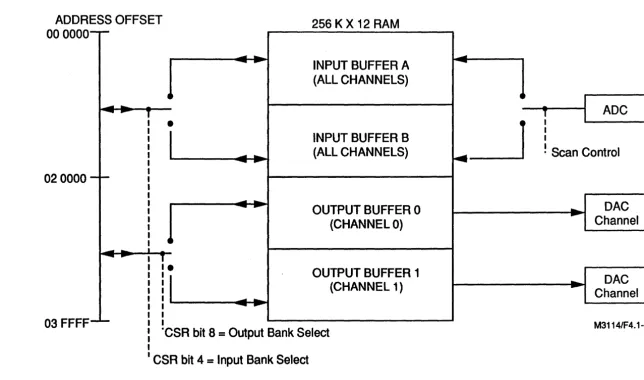
3.5 DATA BUFFERS
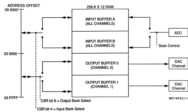
3.5.1 Input Buffers
Digitized inputs are stored in on-board dual data·buffers (Figure 3.5.1-1), which share 128 Kwords of 12-bit wide Dynamic RAM (DRAM). The upper 4 bits of each data word are appended during VMEbus access as a sign extension. Digitized data accumulates within only one buffer at a time. Addressing of buffer memory is controlled by the ADC address counter for ADC access, and by the VMEbus through the VME address buffer for VMEbus access. The CSR permits either buffer to be selected for VMEbus access, or for both buffers to be removed from the VMEbus address space.
The BLOCK SIZE input from the Input Control Register (ICR) establishes the size of each buffer from 2 words to 64 Kwords, in 15 equal binary steps. Maximum scanning rate is controlled by the SCAN RATE output of the ICR from 1 kHz to 125 kHz, in seven equal binary steps. The ADC address counter halts and generates an END SCAN signal when the ADC conversion count matches the BLOCK SIZE. END ADC SCAN causes the ADC timer/sequencer to set a RST ADC ADDR flag which can be programmed to generate an interrupt request. END ADC SCAN also sets an ADC SCAN COMPL flag which is monitored through the SSR.
Buffer operation can be programmed for either single scan operation, in
which AID conversion activity ceases after a single buffer is filled, or for continuous
operation, in which the accumulated data alternately fills each buffer. Data is stored in the input buffer in channel sequence starting with Channel 0 and ending when the buffer is full.
3.5.2 Output Buffers
The analog output data buffers occupy the 64-Kword space directly after the input buffers. Like the input buffers, the two analog outputs are represented by two 64-Kword buffers. Prior to operation of the analog outputs, the VME host must preload the output buffers with a sequence of 12-bit data words which represent the required analog output sequence. Analog output Channel 0 values are located in Output Buffer 0, and Channel 1 values are located in Output Buffer 1.
Control operations are the same as those available for the input buffers, except control of scanning rates is extended to the range from 3.8 Hz to 125 kHz, in 15 equal binary steps.
3.5.3 Buffer Arbitration and Refresh
CAl
I
U'I
000000
020000
I I I I I I I I
4
4
4
4
~ ...
--
-
INPUT BUFFER A(ALL CHANNELS)
[image:27.798.100.716.76.443.2]INPUT BUFFER B
... (ALL CHANNELS)
--
--
..
~
-
OUTPUT BUFFER 0(CHANNEL 0)
OUTPUT BUFFER 1
(CHANNEL 1)
~--
--
--03 FFFF
· CSR bit 8
=
Output Bank SelectCSR bit 4 = Input Bank Select
CSR bit 0 = VME-to-Buffers Enable
Figure 3.5.1-1. VMIVME-3114 Memory Buffers
...
--4
u
-
--I
,
ADCI I I I
· Scan Control
..
DAC-
Channel..
DAC-
ChannelM3114/F3.5.1-1
I
U1
o o
6
o ~
...
~
6
3.6 ANALOG INPUT SYNCHRONIZATION
A sync event initiates a single sample and AID conversion of all active input channels (4 or 8). At each sync event, all input channels are sampled, digitized, and stored in the input data buffers.
3.6.1 Sync Mode
A sync selector enables the VMIVME-3114 Board to be operated either asynchronously or synchronously, and in either continuous, single-block, or single-step mode.
3.6.2 Asynchronous Operation
In asynchronous continuous operation, external sync inputs are ignored and a sync event occurs automatically at the rate established by the SCAN RATE input from the ICR.
3.6.3 Synchronous Operation
Synchronous operation produces one conversion of each input each time a sync event occurs. External sync signals at P2 and P5 are identical, and appear at both connectors. During synchronous operation, the SCAN RATE in the ICR establishes only the maximum conversion rate; the actual rate is determined by the external sync source.
The board can be deSignated as either a master or a slave with the MASTER MODE control bit in the CSR (Section 4). A synchronous master is itself controlled by the EXT AD SYNC input or by CSR bit 007. An asynchronous master depends only on the programmed scan rate.
A synchronous slave ignores the EXT ADSYNC input, and instead,
generates an internal sync event in response to the MIS AD SYNC signal from a
master. This feature permits multiple slave boards to be synchronized to a single master. Master and slaves can be interconnected either through a ribbon cable at P5, or through backplane wiring at P2. As many as seven slaves can be controlled by a single master.
3.7 ANALOG INPUT PROCESSING
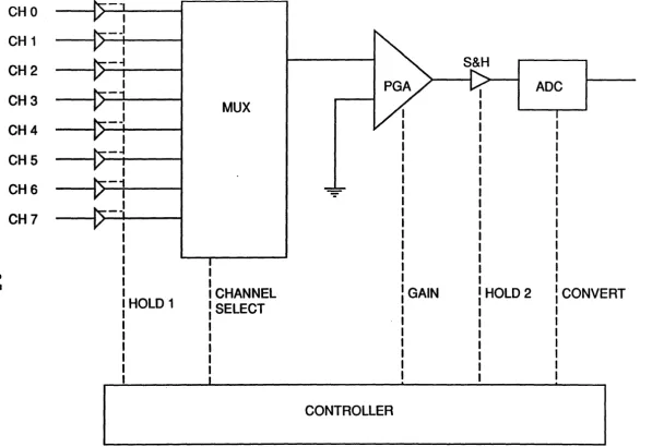
3.7.1 Sampling. Multiplexing. and Digitizing
The VMIVME-3114 Board can be jumper-configured to accept either eight
single-ended or four differential analog inputs. All inputs are sampled
CH2
CH3
CH4
CH5
CH6
CH7
HOLD 1
I I
MUX
I CHANNEL
: SELECT
I
I
I I
I I
-GAIN HOLD 2
[image:29.800.65.663.46.457.2]CONTROLLER
Figure 3.7.1-1. Analog Input Processing (Single-Ended)
ADC
CONVERT
M3114/F3.7.1-1
c.n
o o
b
o ~
~
~
o o
the ADC Timer/Sequencer times out, or in response to an external trigger: Input gain is program controlled by a Programmable Gain Amplifier (PGA) from x1 to x16.
Channel pipelining is used to achieve the maximum possible scanning
rate. The signal level of each channel is stored in a second (ADC)
Sample-and-Hold Amplifier during each conversion, to allow the multiplexer and PGA to settle to the level of the next channel to be digitized.
3.7.2 Data Retrieval
A VMEbus memory read request causes the contents of the selected location to be latched into a memory data latch by the WR VME DATA strobe, after which the memory arbiter/sequencer is available for servicing the next request. ADC data is latched in this manner to prevent a delayed VMEbus data transfer from interfering with the necessary refresh of dynamic memory.
3.7.3 Loopback Testing
To accommodate loopback self-testing of the board, the INPUT MODE control lines from the ICR permit analog input Channels 03 and 07 to be replaced with the two analog output Channels 00 and 01.
3.8 ANALOG OUTPUTS
3.8.1 Digital-to-Analog Converters
The two analog outputs shown in Figure 3.5.1-1 are derived from a dual 12-bit Digital-to-Analog Converter (DAC). Data inputs to the converter are obtained from the 64-Kword analog output data buffers. Converter outputs are deglitched and buffered to permit driving 10 rnA loads. The outputs are jumper-programmable for either unipolar or bipolar output voltage ranges, and can be commanded into either an on-line or off-line mode with the ANALOG OUTPUTS ON-LINE control line from the CSR. Both analog outputs are connected to the I/O connector in the on-line mode, and are disconnected in the off-line mode.
3.8.2 Analog Outputs Synchronization
Synchronization operations for the analog outputs are identical to those for the analog inputs. With the exception of the shared MASTER MODE control, analog output synchronization is independent of input synchronization. An output
external sync event is a falling edge on EXT DA SYNC or eSR bit 011. These
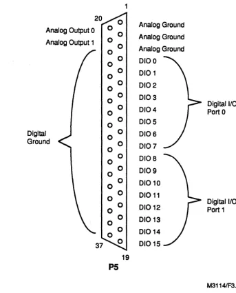
3.9 DIGITAL 1/0 PORTS
Two bi-directional digital I/O ports are provided at the front panel P5 connector (Figure 3.9-1). Each port consists of an octal bi-directional transceiver with tri-state outputs. The direction of each port is controlled by the associated DIRECTIONAL 0,1 OUT line from the CSR. A port is configured as an output port if the associated control line is HIGH, or as an input port if the control line is LOW.
The ports occupy two read/write byte-length registers in the short 1/0 space
(Section 4).
3.10 POWER CONVERTER
Electrical power for the analog networks is supplied by a single DC-to-DC Converter which converts 5 VDC logic power from the VMEbus into isolated and regulated 15 VDC.
1
Analog Output 0 Analog Ground Analog Output 1 0 Analog Ground
0 Analog Ground 0
0 0100 0
0 0101 0
0 0102 0
0 0103
0 Oigitall/O
0 0104
0 Port 0
0 0105 0
Oigital 0 0 0106
Ground 0
0107
0
0 0108 0
0 0109 0
0 01010 0
0 01011
0 Oigitall/O
0 01012
0 Port 1
0 01013 0
0 01014
01015 19
P5
[image:32.620.101.445.59.485.2]M3114/F3.9-1
SECTION
4
PROGRAMMING
4.1 INTRODUCTION TO CONTROLLING THE VMIVME-3114 BOARD
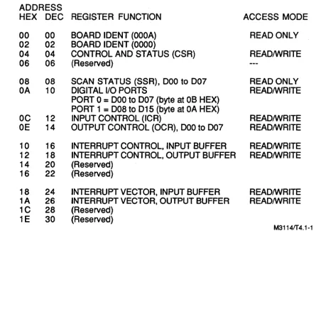
Control of the VMIVME-3114 Board takes place in the VMEbus short I/O space. All short I/O registers are listed in Table 4.1-1.
Four 64-Kword data buffers in the standard or extended address space contain the input data from the eight analog input channels, and the output data for the two analog output channels. VME access to the buffers is controlled by a control bit in the Control and Status Register (CSR), and is disabled when the board is reset. One input buffer and one output buffer are available simultaneously to the VMEbus. The CSR selects one input buffer and one output buffer for VME access (see Figure 4.1-1).
When enabled, the input/output buffers occupy 128 Kwords of contiguous address space, with the lower 64 Kwords representing one of the two analog input buffers, and the upper 64 Kwords representing one of the two analog output buffers. The buffers support both read and write data transfers for 000 through 011.
Analog input data is accumulated in the two analog input data buffers. Block size, scanning rate, synchronization, and all other control functions associated with the analog input data, are controlled and monitored by the short I/O registers. An interrupt can be programmed to occur when an input block is filled.
Analog output data is obtained by scanning the two analog output buffers,
after the buffers are loaded from the VMEbus. Block size, scanning rate,
synchronization, and all other control functions associated with the analog outputs, are controlled and monitored by the short I/O registers. An interrupt can be programmed to occur when the scanning of an output block is completed.
Two digital I/O ports also are controlled through the short I/O registers.
4.2 BOARD IDENTIFICATION REGISTER
The Board Identification Register (BID) contains the board identification code (OOOA 0000 HEX) for the VMIVME-3114 Board, and occupies two words within the short I/O space.
Table 4.1-1. VMIVME-3114 Short I/O Register Map
ADDRESS
HEX DEC REGISTER FUNCTION ACCESS MODE
00 00 BOARD IDENT (OOOA) READ ONLY
02 02 BOARD IDENT (0000)
04 04 CONTROL AND STATUS (CSR) READIWRITE 06 06 (Reserved)
08 08 SCAN STATUS (SSR), 000 to 007 READ ONLY
OA 10 DIGITAL I/O PORTS READIWRITE
PORT 0
=
000 to 007 (byte at OB HEX) PORT 1=
008 to 015 (byte at OA HEX)OC 12 INPUT CONTROL (ICR) REAOIWRITE OE 14 OUTPUT CONTROL (OCR), 000 to 007 READIWRITE
10 16 INTERRUPT CONTROL, INPUT BUFFER READIWRITE 12 18 INTERRUPT CONTROL, OUTPUT BUFFER READIWRITE 14 20 (Reserved)
16 22 (Reserved)
18 24 INTERRUPT VECTOR, INPUT BUFFER READIWRITE 1A 26 INTERRUPT VECTOR, OUTPUT BUFFER READIWRITE 1C 28 (Reserved)
1E 30 (Reserved)
000000
020000
03 FFFF
I I I I I I I I
u
•
I
t
•
I
-
-
...
--_
...
--
...
--
--...
-
-INPUT BUFFER A (ALL CHANNELS)
INPUT BUFFER B (ALL CHANNELS)
OUTPUT BUFFER 0 (CHANNEL 0)
OUTPUT BUFFER 1 (CHANNEL 1)
: ·CSR bit 8
=
Output Bank SelectI
I CSR bit 4
=
Input Bank Select [image:35.799.71.715.72.451.2]CSR bit 0 = VME-to-Buffers Enable
Figure 4.1-1. VMIVME-3114 Memory Buffers
-
-t
~~
I
I
,
ADCI I I I
. Scan Control
....
DAC-
Channel_
...
DAC-
ChannelM3114/F4.1-1
U1
o o 6
o
~
~
~ 6
4.3 BOARD ADDRESS AND ACCESS MODE
Programmable address jumpers permit the short lID registers to be located on any 16-word boundary within the VME short lID address space. Access mode may be programmed for supervisory, nonprivileged, or both.
Jumpers also are provided for locating the input/output data buffers on any 20000 (HEX) word boundary in either the standard or the extended VME address space. Selection of board address and access mode is described in Section 5.
4.4 CONTROL AND STATUS REGISTER (CSR)
CSR functions are summarized in Table 4.4-1. All Control Register bits are mapped directly to the Status Register. The CSR provides control and monitoring of the following board functions:
a. Synchronization modes b. Buffer selection and control c. Scanning modes
d. Analog outputs ON or OFF e. Direction of digital lID ports f. Board self-test
g. Self-test LED h. Board reset
4.5 ANALOG INPUT DATA BUFFERS
ADC data is accumulated in two data buffers, referred to as Buffer A and Buffer B. Input data accumulates initially in Buffer A until the Buffer A data block is filled. Accumulation then transfers to Buffer B. Channel data is contiguous, beginning with Channel 0 at location zero and proceeding consecutively through all active channels (4 or 8). The CSR directs VMEbus access to one of the two buffers. Location of the buffers in the VMEbus address space is controlled by address jumpers. The size of each buffer is fixed at 64-Kwords, but the size of the active data block within each buffer is programmable from two words to 64-Kwords.
4.5.1 Buffer Selection
LOGIC STATE CONVENTION
TO AVOID AMBIGUITIES IN REFERENCES TO LOGIC LEVELS, THIS DOCUMENT USES THE CONVENTION THAT A DATA BIT OR CONTROL LINE IS "SET" WHEN IT IS IN THE "ONE", OR HIGH STATE, AND IS "CLEARED" WHEN ''ZERO'' OR LOW.
Table 4.4-1. VMIVME-3114 Board Control and Status Register (CSR) Functions
015014013012011 010009008007006 DOS 004 003 002 001 000
1 byte 4---I---byte 5---1
MSB CONTROL and STATUS REGISTER (CSR) DATA FORMAT LSB
CONTBOLand STATUS
BII NAME
000 ENABLE BUFFER ACCESS
001 DISABLE OUT
002 MASTER MODE
003 SOFTWARE RESET
004 SELECT INP BUFFER B
005 INPUT SYNCHRONOUS
006 INPUT SINGLE SCAN
007 INPUT SINGLE STEP
FUNCTION
VMEbus access to the data buffers is enabled if 000 is set, or is disabled if 000 is cleared.
Output scanning sequence is stopped (at the last used output levels) and reset if 001 is set, or is enabled if 001 is cleared.
If 002 is set HIGH, the board is a Sync Master and can be used to clock other VMIVME-3114 Boards. If 002 is cleared, the board becomes a Sync Slave, and can respond to sync inputs from a Sync Master. Refer to the descriptions for DOS and D09, and to Section 4.7.
The board is RESET if D03 is set. 003 clears automatically after reset has been completed.
Input Buffer B is selected for VMEbus access if 004 is set; Input Buffer A is selected if D04 is cleared.
The synchronous input mode is selected if DOS is set. Asynchronous (independent) input operation is selected if DOS is cleared.
If D06 is set, the input scanning sequence will halt when the buffer receiving converter data is filled. If D06 is cleared, the sequence will circulate continuously through both input buffers.
When Input Synchronous (bit ~OS) is set, this bit can be toggled to initiate a single frame of AID conversions. Each high-to-Iow transition of D07 will cause a simultaneous sample and a conversion of each of the (4 or 8) input channels. D07 has no effect if DOS is cleared
M3114/T4.4-1/1
Table 4.4-1. VMIVME-3114 Board Control and Status Register (CSR) Functions (Concluded)
CONTROL and STATUS
lUI NAME FUNCTION
D08 SELECT OUTPUT BUFFER 1
D09 OUTPUT SYNCHRONOUS
D10 OUTPUT SINGLE SCAN
D11 OUTPUT SINGLE STEP
D12 DIRECTION 0 OUT
D13 DIRECTION 1 OUT
D14 ANALOG OUTPUTS ON
D15 LED OFF
Buffer 1 is selected for VMEbus access if 008 is set; Buffer 0 is selected if 008 is cleared.
The synchronous output mode is selected if 009 is set. Asynchronous (independent) output operation is selected if 009 is cleared.
If 010 is set, the output scanning sequence will halt at the end of the buffer which is providing output data. If 010 is cleared, the sequence will circulate continuously through both output buffers.
When OUTPUT SYNCHRONOUS (bit 009) is set, this bit can be toggled to initiate the next 01 A conversion for each output. Each high-to-Iow transition of 011 will cause the outputs to be updated from the next locations in their buffers. Digital PORT 0 is configured as an output port if 012 is set, or as an input port if 012 is cleared. Digital PORT 1 is configured as an output port if 013 is set, or as an input port if 013 is cleared. The analog outputs are connected to the 1/0
connector if 014 is set, or are disconnected if 014 is cleared.
The "Fail" LED is OFF if 015 is set, or is ON if 015 is cleared.
4.5.2 Location
The input buffers are located at the VMEbus address selected by programmable jumpers, as described in Section 5. The input buffers can be located on any 20000 (HEX) word boundary within the standard A24 or extended A32 address space.
4.5.3 Enabling
Access to the data buffers is enabled by setting CSR control bit 000 HIGH. 000 is cleared during a reset operation.
If the CSR bit 000 is cleared, VMEbus attempts to access data buffers are ignored. This feature allows multiple VMIVME-3114 Boards to share a common region in the VMEbus address space. It also serves to hide the buffer RAM from systems which search for active RAM during their power-up configuration.
4.5.4 Block Size
A data block is the active portion of a data buffer, and has the same base address as the buffer. Input data block size is controlled by the Input Control Register (ICR) shown in Table 4.5.4-1. ICR bits 000 to 003 adjust the size of the active analog input data block from two words to 64 Kwords in 15 equal binary steps. Only the active region is filled with data during a scan. All 64 Kwords may be reached by the VMEbus.
4.5.5 Data Format and Coding
Data from the AOC is stored in the input buffers in 12-bit right-justified format, as shown in Figure 4.5.5-1. Coding of the data is two's complement if the Two's COMPLEMENT jumper is installed, or is binary if the jumper is removed (refer to
Section 5). The data coding selected by the Two's COMPLEMENT jumper also
applies to the analog outputs.
4.5.6 Block Transfers
Block transfers are supported to a maximum of 128 words per transfer.
4.6 INPUT SCAN CONTROL
4.6.1 Single-Scan and Continyoys Modes
CSR bit 006 selects the input single-scan operating mode when set, or the continuous mode when cleared. In the single-scan mode, digitizing ceases when Buffer A is filled, and will not resume until the scan address is reset by ICR bit 007 or by CSR bit 003. Buffer B is not used in single-scan mode.
Table 4.5.4-1. Input Control Register (ICR)
000 to 003 .... INPUT BLOCK SIZE
003 002 001 000 DATA BLOCK SIZE (HEX)
o
0 0 0 2 WORDS (Note 1)o
0 0 1 4 (Note 1)o
0 1 0 8 (Note 1)o
0 1 1 10o
1 0 0 20o
1 0 1 40o
1 1 0 80o
1 1 1 1001 0 0 0 200
1 0 0 1 400
1 0 1 0 800
1 0 1 1 1000
1 1 0 0 2000
1 1 0 1 4000
1 1 1 0 8000
1 1 1 1 10000
004 to 006 .... AID CONVERSION RATE (TOTAL FOR ALL INPUT CHANNELS)
006 DOS 004 CONVERSION RATE (CONV/SEC)
o
0 0 125.0 kHzo
0 1 62.5 kHzo
1 0 31.2 kHzo
1 1 15.6 kHz1 0 0 ~8kHz
1 0 1 3.9 kHz
1 1 0 1.9 kHz
1 1 1 0.9 kHz
007 .... DISABLE IN H When this bit is set, input scanning is disabled (halted).
008 to 010 .... INPUT GAIN 010 009 008 0 0 0
o
0 10 1 0
o
1 11 1 1
011 to 012 .... INPUT TEST MODE
When it is cleared, the scan will begin with the first location of buffer A.
INPUT GAIN x1
x2 x4 x8 x16
012 011 INPUT DATA CHAN 03 INPUT DATA CHAN 07
INPUT 07 (Normal Operation) OUTPUT 01
o
0 INPUT 03o
1 OUTPUT 001 0 OUTPUT 00 ANALOG RETURN
1 1 ANALOG RETURN ANALOG RETURN
NOTE 1: If the block size specified is less than the channel count, channel count is truncated to block size. The default block size is 8 which allows all 8 channels to be stored.
ADC DATA FORMAT
MSB LSB
D1S D14 D13 D12 Dll 010 D09 DOS D07 D06 DOS 004 D03 002 DOl DOO
I
*
I*
I*
I*
I 0 I 0 I DID I D I 0 I D I 0 I DID I DID I*
=
Zero (binary) or extended sign (two's complement).ADC CODING
================================================================
UNIPOLAR RANGE
INPUT
+FS-1 LSB +1/2 FS +1 LSB
STRAIGHT BINARY
a
to +5v
D15 DOO+4.9988
v
+2.5000v
+0.0012v
0000 1111 1111 1111 0000 1000 0000 0000 0000 0000 0000 0001
================================================================
BIPOLAR RANGE OFFSET BINARY
INPUT 5
v
D15 DOO+FS-1 LSB +4.9976 V 0000 1111 1111 1111 +1/2 FS +2.5000 v 0000 1100 0000 0000 +1 LSB +0.0024 V 0000 1000 0000 0001 ZERO 0.0000 V 0000 1000 0000 0000 -FS+1 LSB -4.9976 V 0000 0000 0000 0001 -FS -5.0000 V 0000 0000 0000 0000
================================================================
BIPOLAR RANGE TWO'S COMPLEMENT
INPUT 5 v D15 DOO
+FS-1 LSB +4.9976 V 0000 0111 1111 1111 +1/2 FS +2.5000 v 0000 0100 0000 0000 +1 LSB +0.0024 V 0000 0000 0000 0001 ZERO 0.0000 V 0000 0000 0000 0000 -1 LSB -0.0024 V 1111 1111 1111 1111 -FS+1 LSB -4.9976 V 1111 1000 0000 0001 -FS -5.0000 V 1111 1000 0000 0000
[image:41.621.80.527.88.589.2]================================================================
M3114/F.4.S.S-1Figure 4.5.5-1. ADC Data Format and Coding
If continuous operation is selected, the accumulated data alternately fills each buffer, transferring to the opposite buffer as each buffer is filled. To prevent the overwriting of data in either buffer when the opposite buffer becomes filled,
VMEbus transfer rates must exceed the conversion rate. In asynchronous
operation, the AID converter runs at the rate selected by ICR bits D4 to D6. For example, when these bits are all zeros, the converter runs at 125 kHz and each channel is converted at 31.25 kHz (4 channels) or 15.625 kHz (when 8 channels are configured). In synchronous operation, ICR bits D4 to 06 set the maximum conversion rate.
As each buffer is filled, the event can be determined either by polling the AID
SCAN A flag in the SSR, or by programming an interrupt to occur when either buffer becomes filled (refer to Section 4.9 "Bus Interrupter"). The AD SCAN A flag is set when the ADC is filling Buffer A, and is cleared when filling Buffer B.
4.6.2 AID Conversion Rate
The maximum conversion rate for the ADC is selected by the ICR, which is
shown in Table 4.5.4-1. ICR control bits D04 to 006 adjust the maximum
conversion rate in seven equal binary steps. In the asynchronous or independent mode of operation, conversions occur automatically at the selected maximum rate. In the synchronous mode, sampling is initiated by an input sync event. Input sync events are identified in Table 4.6.2-1.
The maximum sampling rate or sync rate equals the conversion rate divided by the number of input channels, and has a maximum value of 31.25 kHz if the board is configured for four input channels, or 15.625 kHz for eight input channels. The number of channels is four for differential operation, or eight for single-ended operation. External sync rates may be a fraction of a percent higher than this, but if they are too high, then every other sync will be missed.
4.6.3 Scan Status Register (SSR) Monitored Functions
Functions monitored by the SSR include the status of the scanning
sequence, and the states of configuration jumpers. Scan status monitored
functions are described in Table 4.6.3-1. The SSR is a read only register.
4.7 INPUT SYNCHRONIZATION MODES
4.7.1 Synchronous Operation
Synchronous operation of analog inputs is selected by setting CSR bits 005 and 002 HIGH. In this mode, all input channels are sampled and digitized once for each input sync event. A sync event is a falling edge on either the EXT AD SYNC input or eSR bit D07. These inputs are OR-ed together, so bit 007 must be kept low when the external input is used. When the EXT AD SYNC input is not used, a built-in resistor pulls it low. If CSR bit D02 is set but eSR bit 005 is cleared, the
Table 4.6.2-1.
CSR bits Mode
OCS.OO2
0 0 Asynchronous
(free running)
0 1 Async. Master
1 0 Slave
1 1 Ext. Sync Master
Analog Input Synchronization Modes
Controlling Sync Eyent
On-board rate generator
Is MIS AD SYNC
driven? NO
On-board rate generator YES
MIS AD SYNC input NO
Falling edge on YES
EXT DA SYNC input or CSR bit 007
M3114rr4.6.2-1
================================================================
SSR bit
000
001
002
003
004 005
006
007
008 ... 015
-Table 4.6.3-1. Scan Status Register (SSR)
NAME DESCRIPTION
AD SYNC ROY The analog inputs are ready for the next
sync event when this is HIGH.
AD SCAN A The results of the next AID conversions will
be sent to buffer A when this is HIGH, or to buffer B when this is LOW. Bit 001 also goes LOW when a single-scan input scan finishes.
AD SCAN COMPLETE This bit is set the first time an input scan
has filled buffer A. It is cleared by a reset from ICR bit 007 or CSR bit 003.
OA SYNC ROY The analog outputs are ready for the next
sync event when this is HIGH. Bit 004 is reserved.
DA SCAN COMPLETE This bit is set the first time the output scans
reach the ends of their buffers. It is cleared by a reset from CSR bit 001 or CSR bit 003.
STRAIGHT BINARY The AID and DIA converters are using
straight binary andlor offset binary, as
determined by jumper J1, when bit 6 is
high. When this bit is LOW, the
VMIVME-3114 is. configured for two's complement data.
OIFF INPUTS HIGH indicates that four differential inputs
are being scanned, instead of eight single-ended inputs.
These bits are reserved.
M3114rr4.6.3-1
[image:43.624.64.533.76.733.2]The maximum sync event rate may not be more than the ICR's preset conversion rate, divided by the number of channels used. For instance, the ICR defaults to a conversion rate of 125 kHz. In this case, the sync event rate is limited to 15.625 kHz in a-input (single-ended) mode or 31.25 kHz in 4-input (differential) mode.
4.7.2 Asynchronous <Independent> Operation
The asynchronous analog inputs operating mode is selected by clearing CSR bit DOS. External sync inputs are ignored in this mode, and digitizing of the analog inputs occurs automatically at the selected conversion rate in the ICR. If CSR bit 002 is set, the VMIVME-3114 will drive M/S AD SYNC for other boards to sync to.
4.7.3 Myltiboard Synchronization
Multiple VMIVME-3114 Boards can be configured to provide synchronized, simultaneous sampling of analog inputs. This feature is implemented by designating one of the boards as a master, and by designating the remaining boards as slaves. External cabling at the P2 or P5 connectors provides the necessary hardware interconnections for multiboard synchronization, the control signals for which are described in Sections 3 and 5. A single master can control as many as seven slaves.
Master/slave behavior is program-controlled by CSR bit 002 (MASTER MODE). A master may operate in any sync mode. It will retransmit its sync signals (both input and output) to the slaves. A slave will follow the input sync signal (MIS AD SYNC) if bit DOS of its CSR is set. It will run asynchronously if bit DOS is clear. CSR bit 002 also affects the OUTPUT master/slave behavior.
4.8 ANALOG OUTPUTS
The VMIVME-3114 Board provides two dynamic analog output channels, both of which use Digital-to-Analog Converters (DACs) to convert 12-bit digital values from scanned data buffers into sequences of analog voltage levels. The data buffers can be: scanned automatically, single-stepped, or synchronized to either an external sync signal or to another VMIVME-3114 Board. A self-test multiplexer permits the analog outputs to be routed to the analog input multiplexers for loopback self-testing.
4.8.1 Output Buffers
Two 64-Kword buffers are dedicated to the two analog output channels. Output 0 values are obtained from Output Buffer 0, and Output 1 values are obtained from Output Buffer 1. Like the analog input buffers, the active portions of the output buffers are referred to as blocks. The Output Control Register (OCR) determines their size. Both outputs are scanned at the same clocking rate, which also is controlled by the OCR. OCR functions are summarized in Table 4.8.1-1.
4.8.2 Output Scan Control
Scanning of the output buffers is controlled by CSR bits 008 to 011, and by the OCR. CSR output control functions are identical to the corresponding functions for the analog inputs, and are described in Table 4.4-1.
Block size and clocking rates are controlled by the OCR, as shown in Table 4.8.1-1. 000 to 003 control the block size from two words to 64 Kwords in 15 equal binary steps. 004 to 007 adjust the clocking rate from 3.8 Hz to 125 kHz, in 15 equal binary steps. 008 to 015 are not used.
4.8.3 Output Synchronization Modes
Synchronization modes for the analog outputs are identical to those described for the analog inputs. With the exception of CSR bit 002 (MASTER MODE), all output synchronization functions are independent of analog input activity. The maximum sync event rate for the outputs is 125 kHz. The possible input and output sync combinations are shown in Table 4.7.3-1. The output modes alone are shown in Table 4.8.3-1.
4.8.4 Self-Testing the VMIVME-3114 Board
The analog outputs can be monitored through the ADC to provide a closed loop self-test of the VMIVME-3114 Board. ICR control bits 011 and 012 select the self-test mode, as shown in Table 4.5.4-1. The self-test modes permit the analog outputs to be monitored instead of Analog Input Channels 03 and 07. All other control functions are unaffected, and the closed loop test configuration can be applied in both the on-line and off-line analog output modes.
4.9 BUS INTERRUPTER
Interrupts are available to inform a host CPU of progress in the analog input and output scans. There are two interrupt channels. Channel 0 is for the analog input scan. It can do interrupts when the input scan crosses from buffer A to B and vice-versa. Channel 1 is the analog output end-of-buffer interrupt.
Table 4.8.1-1. Output Control Register (OCR)
000 to 003 .... OUTPUT BLOCK SIZE
003 002 001 000 DATA BLOCK SIZE (HEX)
o
0 0