The
Tarbell
Floppy
Disk
Interface
V'
~
PLUGS TARBE.LL INTO
COMPUTER FLOPPY
DISK
I NT E.RF"ACE
POWER SUPPc..Y
r---T
I
--'.
\.-.0"" .l1' ~
.,.
l.-I-SWITCH FUSE
-~
50-PIN CABL£.
rL
::0"
1i~1JAJ!
20620 SOUth Leapwood Avenue. SUiIe P~~/
Carson,Califomia 90746A
)
, NTe.RF'ACE CON NE.CTOI\v
FLOPPY •
DI5K
PRIVE(S)
TABLE OF CONTENTS
1 OVERVIEvv
1-1 Introducing the Tarbell Floppy Disk Interface 1-2 Operating Instructions/General Notes
1-3 Important Cautions 1-4 Software Support
2 THEORY OF OPERATION
(helpful to read before assembly or operation but not a necessity)
3 ASSEMBLING THE INTERFACE BOARD (KIT UNITS)
3-1 Parts Drawing 3-2 Parts List
3-3 Step-by-step Assembly
4 SETTING THE JUHPERS
4-1 Using the Jumper Pads 4-2 Jumper Set-ups for
a) b) c)
CDC BR803A Innovex 210 Innovex 410
5 CHECKOUT
5-1 Visual Inspection 5-2 Installing the 1771
d)
e) f)
GSI 110
Per Sci 270/277 Shugart SA 800
5~3 Interconnecting Drive and Interface 5-4 Operational Tests
6 FIRM1'JARE AND DRIVERS
6-1 The HardwFlre Bootstrap 6-2 Writing Driver Routines
7 REFER,."SNCE INFOR~·1ATION
7-1 IC Pinouts and Ch~racteristics
7-2 1771 Data Sheet
7- 3 Parts P lacemen t (.1\ssembly Diagram) 7-4 Schematic
The Tarbell Floppy Disk Interface is a programmed-data-transfer (not DMA) device. It plugs into your IMSAI or ALTAI R* computer, and is designed to work with a variety of standard-size floppy disk drives. It includes a 32-byte ROM bootstrap program, which is automatically enabled when the com-puter RESET button is pushed, and which switches itself out after the bootstrap hasrun. In th is way, no part of your memory needs to be dedicated to Read-Only-Memory (ROM). The interface runs at the standard speed of 250,000 bits per second, and the normal formatted capacity per diskette is 243 kilobytes. Places for two connectors are provided on the board. One 50-pin header connector and a cable with the mating connector are provided with the interface kit. There are four extra IC slots to allow you to do your own thing, and the connector pins come out to jumper pads, so you can adapt to different drives. The manual has the connections detailed for popular drives. An on-board dip-switch is used to select the device address, disable the bootstrap, and write-protect. Circuitry is included to run up to four drives, and eight can be accessed by using the spare IC slots.
The Tarbell Floppy pisk Interface and other related items can be bought in pieces, so that it's not necessary to make a single large outlay of cash. Because of this policy, the 6-month warranty will be limited to only those items traceable to Tarbell Electronics. Notice that we will be offering the CP/M floppy disk vperating system, which is described on another page. An owner's manual for the interface is included with the kit or the bare board, and is also available separately.
Floppy Disk Interface Kit
CP/M Operating System (on disk) CP/M System Manual Set (6) BASIC-E Compiler Manual
Innovex Model 410 Floppy Disk Drive Power Supply for I nnovex 410
GSI 110 Floppy Disk Drive Floppy Disk Interface Manual Bare Floppy Disk Interface Board Kit with all parts except 1771 Western Digital 1771 FDC IC Assembled Floppy Disk Interface PerSci 270 Dual Floppy Disk Drive Power Supply for PerSci 270 Blank Formatted Diskette BASIC-E Source Listing (PL/M) Additional Charge for Special Cable Package of IC Sockets (35)
190.00 70.00 25.00 5.00 575.00 75.00 525.00 5.00 40.00 125.00 80.00 265.00 1130.00 125.00 10.00 9.00 10.00 10.00
NOTE: These prices are pre-liminary, and are subject to change without notice. There are no discounts for complete systems; just add the prices to-gether to find the total for your purchase.
Since Tarbell Electronics does not wish to get into the business of selling complete systems, we en-courage you to buy your system, including the floppy disk drive, from your local dealer. If you add up the prices of the first six items, however, you can see that a complete floppy disk system including software and hardware can be had for less than a thousand dollars. Note thatthe Tarbell Floppy Disk Interface is not designed to work with double-density or mini-floppys, although it will work with multiple and double-sided drives. The drives that it has worked with so far include the Shugart 800/801, the I nnovex 410, the I nnovex 220 (modified by a jumper change), the GSI 110, the CDC 803, and the PerSci 270.
The first deliveries were made July 2, 1977. Delivery from the factory is 3-4 weeks after receiving your order,. and individuals must send cash in advance. For faster delivery, check with your local dealer .
... A L TAl R is a trademark/tradename of M ITS, Inc.
OPERATING INSTRUCTIONS
One nice thing about using a floppy disk is that the operation of the hardware is fairly simple:
1. Turn on computer power. 2. Turn on disk power.
3. Put a diskette into the drive and close the door. 4. Press the reset button on the computer.
S. Press the run button on the computer.
At this time, the hardware bootstrap routine automatically reads in the first sector of track zero, and runs it. This 128 byte module contains a more sophisticated loader which brings in the main operating system and runs it. Therefore, you should see the header that the operating system prints when it first comes up. In CP/M, this is something like "CPM Vl.3". From this point on, you need to refer to your manual on CP/M (or whatever operating system you're using).
When you're all done, the shut-down procedure is as follows:
1. Open the disk drive door and remove the diskette. 2. Turn off the power to the disk drive.
3. Turn off the computer power.
GENERAL NOTES ABOUT USING YOUR DISK SYSTEM
1. In general, floppy disk drives are a very reliable method of storing data if nothing else goes wrong in the computer. As with any external medium, however, there will be some errors. These are normally detected by the interface and the software. The manual on your disk drive should have some figures as to the reliability of your particular unit. As a rule, you can expect the Tarbell floppy disk interface and your floppy disk drive to work for many days at a time without an error.
2. On the other hand, remember that your floppy disk interface is an on-line device; that is, the computer can write onto it any time, unless the write-protect is on. This has its advantages, but i t also means that the disk is always subject to wipe-out,
********
IMPORTANT CAUTIONS********
1. All RAM boards used in this disk operating system must have no wait states.
2. Take extreme care in handling the integrated circuit. Being a MOS device, i t to destruction from static charge induced by handling--and it's expensive.
FD1771B-Ol is liable excessive
3. Before removing or installing the floppy disk interface board or any board in your computer, turn off the power and wait for at least ten seconds to let the capacitors discharge.
4. Before turning the computer power or the disk power on or off, be sure that the disk door is open, and preferably that the diskette is removed--so any transiets won't wipe out the disk.
5. Always turn on the computer power before the disk power, and turn off the disk power before the computer power.
THEORY OF OPERATIO~
The internal operation of a floppy disk system is probably the most compl,i.cated part of a micro-computer system. The hardware and software interact very closely. For best understanding, you should be familiar with both the 8080 machine/assembly language, and the common logic operations. Some understandinq of the S-lOO bus is afso desirable. Remember to take into account any differences in your system's I/O setup as you follow the circuit.
Since the Tarbell Floppy Disk Interface is designed around the Western Digital 1771 Floppy Disk Integrated Circuit, it would be helpful to skim over the data sheets (reproduced in the appendix with the manufacturer's permission). The main thing is to get a feeling for what the 1771 does in order to get a perspective of how it fits into the circuit.
ABOUT READING THE SCHEMATIC: note that lines of most drives are true when low--that is, a low voltage is a logic one. Active low lines have an asterisk following their name (e.g., RDY*). The convention of this schematic is that a darkened dot is a possible connection to a floppy disk drive; an open circle is a pad for a possible jumper wire; a little square with a number in i t is a pin on the laO-pin 8-100 bus; and a line with none of these, but a name close to it, is a connection to another line with the same name.
To see what we need in the interface, let's see what it must connect to on each side. On the computer side, we have two simple instructions: input a byte
(IN), and output a byte (OUT).
On the side of the floppy disk, we have many things to be concerned with. First, the going to and from the floppy drive are serial at a time). Thus ,-,re must have some ""'T?Y
parallel computer data to serial data on side.
different data lines (one bit to convert the drive
Next, the drive has several control lines. These are lines that tell the drive ""'That to do. For example, there are two lines to tell the drive to move the head in or out. There's another line that tells the drive to engage the head aoainst the disk surface (normally the head is not in contact to reduce wear on the disk and on the head). Another control line is usually used to reset the drive electronics and return the head back to the zero (outside) track. There's a set
destroying some or all of the information on it. All i t takes is a software error, power-line glitch ora temporary hardware malfunction to lose manyhbtirS, days, and even weeks of work if you only have that single copy.
It is therefore desirable to keep frequent back-ups of
your files. This can be done by copying files to another diskette or to cassette. In this way, only the information entered since the last backup can be destroyed.
3. When first using any operating system, including CPM, run it in the write-protected mode for a little bit. Then make a back-up copy as soon as possible.
4. Note that CP/M always loads a program for execution at 100 hex. If i t is desired to run a program at zero, such as basic, i t must first be loaded at 100 hex and then moved down.
5. When the bootstrap switch (7) is on, a reset will gate the bootstrap program onto the bus. Even programs that run in·other parts of the memory may be adversely affected if you atterr.pt to run theM before the hootstrap is disabled. Although the bootstrap is normally disabled automatically, there may be times when you want to disable it manually. This can be done by putting front panel data switch 5 to the up position and doing an examine, or by turning off dip-switch 7.
6, There is a difference in the reliability of different manufacturer's diskette media. We at Tarbell Electronics have not yet decided which ones are the best. Ask your friends who know. Try several kinds. You will find that you get more errors on some than on others.
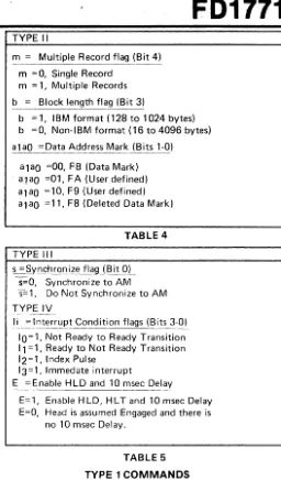
7. Diskettes are usually initialized by the manufacturer in some way. IBM format dictates a certain sequence of information about track number, sector number, fill characters, etc. on each track. The proper format for IBM compatibility is shown in the 1771 data sheet.
of lines on some drives to select one drive out of several on a "daisy-chain" bus.
Still other lines tell write, and to write these control lines interface, normally at
the drive whether to read or with how much current. All of need to be driven by the high-current TTL levels.
There in the lines drive.
are also a set of status lines which originate drive and come back to the interface. These tell the interface what is going on in the
There is usually a ready line, set true when the drive is up to speed and a disk is in place. The index line has a pulse on i t that indicates when the index hole in the diskette passes by the opening made for it. This is used by the interface to determine which sector is which on the track.
Some drives have a way to detect a notch cut out of the diskette holder, which indicates that disk is not to be written upon (write protected). There is usually a line going back to the interface to indicate this condition, so the controller can feed the information back to a program, and so the interface won't try to write to the disk. Another line indicates when the head is at track zero. Some drives have a write-fault flip-flop, which is set by an attempt to write when i t was not possible. The output of this flip-flop is sometimes a status line.
You may begin to see now one reason why the floppy disk system is complicated: there are a lot of status and control lines to keep up with.
DEVICE-SELECTION (BOARD ADDRESSING)
The first task of the interface is to recognize when the program sets the hardware for a read or a write operation to the disk. Selection circuitry is used to recognize 5 of the 256 possible I/O addresses. In this way, the floppy disk interface will respond only to the I/O instructions given to it, and not to those intended for other interfaces. The components associated with this process are located in the lower part of the schematic, slightly to right of the middle. These are dip-switch S-l (5 positions used here), mi8l3l U25 (a 6-bit comparator), 74LS32 OR gates U27, a 3-input NAND gate from 74LSIO U43, plus a few inverters.
The comparator checks for a match bet~Teen the 5 high bits of the device address (lines A3, A4, AS, A6, and A7) and the bit pattern set on the dip switch. If the five lines (BI-B5) on the left each have the same logic level as the ones on the right (TI-T5), then the
comparator output at pin 9 goes low, indicating the disk interface is being selected. For any other combination, pin 9 goes high, and the instruction on the bus if left for some other interface.
Since the lower three address bits (AO, lAl and A2) can be anyone of eight combinations, eight I/O ports out of the possible 256 are selected for use with the disk interface. Which set of eight depends on the upper five bits selected by the dip-SVlitch.
From now on, let's assume that the upper five bits match--that is, an input or output instruction has been put on the bus with the correct address for the disk interface, so that the comparator output goes low). Note that this output goes up to an input on each of blO OR gates (these gates are dravrn as AND gates, to indicate that because of the inverted input signals, the AND function is beinq performed--ie. when both inputs of a gate are low, the output of the gate is low. On the top one of these blO gates, pin 4 is connected to address lineA2. So when A2 is low
(and we've already said pin 5 is low), the gate's output at pin 6 is also low (active). This line is called CS*, for chip-se1ect-not, and is connected to the 1771 chip-select line. This line, then, will be active anytime there is a transfer to be made between the computer and the 1771.
A similar decoding scheme sets each of the other individual operations. The table below shows how the address decoding scheme is set up, and the lines that are active for each situation.
A2 Al AO FUNC'1'ION OUT FlJ1'JCTION IN LINE ACTIVE
0 0 0 Command to 1771 Status from 1771 CS*
0 0 1 Track to 1771 Track from 1771 CS*
0 1 0 Sector to 1771 Sector from 1771 CS*
0 1 1 Data to 1771 Data from 1771 CS*
1 0 0 decoded by U56 see table below U43-6,U27-8 1 0 1 Not used Not used
1 1 0 ~Jot used lJot used
1 1 1 Not used Not used
Notice that no further decoding of address bits AO and Al is required to perform the first four functions in the table. That's because these functions are decodeo. inside the 1771. ~otice also that U-55 pin 4 is fed by U3-3, which is true when PDBIN is hig~ and SINP* is low (both true). This indicatps to the 1771 that an input (1771-to-computer) operation is taking place. U55-2 is fed by U43-6, which is true 0hen an output
(computer-to-1771) transfer is taking place; PWR* and SOUT are both true.
If A2, Al other five
and AO are 1, 0 and 0 respectively, and the I/O address bits match the setting of
[image:9.621.68.578.137.776.2]switch Sl, gates U44, U43, U27 and U25 (all in lower right) pull line IO* down. This line, along with an active low signal from U43 (when SOUT and PWR* inverted are true) enables U56 (a 3-to-8 line decoder). This is the fifth state given in the table above. Enabling U56 allows i t to pull one of its output lines low in accordance to the state of the three least-significant data-out lines, DO, Dl, and D2 which are the inputs to the decoder. Only the top three of the available 8 outputs are used: Y5, Y6, and Y7. This actually decodes the bottom three combinations of DO, Dl, and D2, since these lines are active low (inverted). The table below ShO~TS what these combinations are used for:
D2 Dl DO 0 0 0 0 0 1 0 1 0
BUFFERS
Y
7 6 5
U56-7 9
10
Once the board has decoded, the actual series of buffers.
been data
FUNCTION DESCRIPTION
Pad E-32, can be used to pulse RST* line Inverted, then to E-14 for SO* line
Strobes data bits 4,5,6,7 into latch U40
selected and the operation transfers are done by a
The buffers in this interface have three main purposes: 1) To protect the expensive LSI chip (1771 IC) from voltage transients on external lines; 2) To provide sufficient drive current for the lines that need it; 3) To provide multiplexing (s'\ATitchinq) of two data paths. The signal th~t comes out of a buffer is either the same signal that '\ATent in or simply the inverted form of what went in.
Looking in the lower left corner of the schematic, we see a row of 12 buffers. All the data inputs for these buffers come from the disk drives(s), ~nd all the outputs go someplace in the interface. The line on the top of each buffer is the control line. \\1hen this line is low, the buffer is active--that is, the output equals the input for that buffer. When the control line is high, the output for that buffer is floating in an open state so i t does not affect any connecting circuits. Notice that every other buffer is hooked to the same control line, and that there are two main control lines. One control line activates the buffers that have signals from drive number 0, the other control line activates the buffers that have signals from drive number 1. Thus the buffers are acting as a l2-1ine to 6-line multiplexer. This multiplexing operation is only necessary if there is more than one drive, and the drives do not have multiplexers built in (most late-model drives do).
Also notice the 120 ohm these buffers. They
resistors hFtve tyqo
2-4
on the purposes.
inputs of
match the normal low line impedance so that ringing caused by reflections will be minimized. The other is to make i t difficult for external noise to provide enough current to cause a false signal on the line. The six outputs of these buffer pairs will be called by their signal name, while their inputs are named by the signal line plus the number of the drive (i.e.,
ROY, RDYO, and RDYI).
Next move your eye on the schematic up and slightly to the right. There is a row of five 7438 2-input NAND high- current open-collector gates. These are used as buffers in this interface. Their main advantage is that they are capable of supplying the high current required by the floppy drive(s). They also can double as NAND gates. As set by the jumpers, they are used to send the appropriate signals from the 1771 to the various disk control lines (see the 1771 data sheet and your drive's manual for a full explanation of the various lines). If both inputs to these gates are a logic high, the output is low. To the right, in the
~iddle of the schematic, are seven more of these 7438 buffers. These too go to the drive(s).
About two thirds of the way to the right near the top of the schematic, there are two rows of 8 buffer/inverters each. These buffers link the computer input and output data busses to the 1771 data bus. The inputs to the left row of buffers come from the S-lOO bus. The control lines for all these buffers are connected together. When this control line is low, the data on the output data bus is inverted and gated onto the 1771 data bus. The gates on the right hand side do the reverse: when their control line is low, the data on the 1771 data bus is gated onto the computer's input data bus.
The last set of buffers is on the far right-hand side of the schematic, and is a row of nine non-inverting buffers. Their purpose is to suspend the usual CPU control of the data bus and gate the proper control signals onto the S-lOO status lines to put the bootstrap in operation. When their common control line is low, whatever is on their inputs is gated to their outputs. Once the bootstrap is co~pleted, U43, U34, ~nd U37 relinquish control back to the bus.
Bootstrap is initiated by NOR gate U28 (lower right) recei ving Power On Clea.r (also generated by RESET) from the computer, 'VIThich sets flip-flop U34 (upper right). The not-Q output, if passed by 81 position 5, is the bootstrap signal. This gates those nine buffers, and is used along with a signal from U37
(upper right) to activate U27 (middle) during the read cycle, thus reading from the 82Sl23 memory but writing through the bus to regular RAH.
TIMING CIRCUITS, SEPERATOR, AND PROCESSOR HOLD
At the lower right of the schematic, Ul, U2, U17, U33, U34, U35, and U36 form the clock and data seperator, which operates on the raw data which comes in on the
line wich runs across the very bottom of the schematic. The actual clock oscillator circuit (also lower right) is composed of two sectons of U17 plus the 4MHz crystal Yl. Grounding pin 25 of the 1771
(XTDS*) disables the internal seperator.
On the the 1771 the CPU or XRDY. suspend internal
bottom middle, the INTRQ and DRQ signals from are used to control the run or wait state of through gates U30 and U57 and bus signals PPDY These circuits allow the 1771 to temporarily execution of the next CPU instruction until an process has been completed.
HEAD-LOAD CIRCUIT
The 1771 checks for head-load by looking at the HLT line 10 milliseconds after the HLD line is activated. u41 and U57, in the upper-left corner of the schematic, sample the HLD line and generate the proper delay to allow for the physical head-load time of the drive before passing the signal on to the HLT input of the 1771.
STEP-IN M~D STEP-OUT CIRCUIT
The 1771 signals your drive to step the head in or out by providing a short pulse from the step output and a DIRC output which is high for stepping in and low for stepping out. These signals must be reformatted for many drives, and they must be buffered. The circuitry at U59, U51 and U61, all in the upper left side, perform these tasks.
Most drives require a longer step pulse than is output at pin 15 of the 1771, so one-shot U51 is used to stretch the pulse out. For drives ~f7hich require a step signal and the same polarity direction signal, like the Innovex 410, the other signals are simply buffered and then routed to the drives by the appropriate jumpers. For drives like the CDC BR803A, which require a step-in and step-out line, the jumpers are set to make these circuits decode those signals from the DIRe and step lines.
A few drives require step signals faster than those generated by the 1771. The line into pin 1 of buffer U59 can be driven directly by the computer, and can therefore be pulsed at a nuch faster rate. However,
in this case, the program must number of pulses that this line observing any timing constraints. WRITE DATA, WRITE GATE, TRACK GREATER
keep track puts out,
THAN 43
of the plus
The write data, write gate, and track greater-than-43 signals control the write-to-disk functions. The circuits to control these signals are just above the middle left.
The write-data line contains the actual data mixed with a clock signal. From pin 31 of the 1771, i t goes through buffer U57, and line driver U62, . and then out through the jumpers to the disk. The TG43 line which tells the drive to reduce the head current while writing on the physically smaller tracks is set high when the track number is higher than 43. From the 1771 pin 29, i t goes to U35, where i t can be inverted for drives which require the opposite polarity, and then through driver u62 and the jumpers out to the disk.
The write-gate signal tells the drive that i t is time to start a write operation. It comes out of the 1771 pin 30, is buffered by U57, and NANDed with the write protect signal at U62, where i t goes to the jumper pads and the disk. The write gate sigrial can only go active (low) when switch position 6- of DIP-switch 51 is off, providing a logic 1 to pin 5 of U62. This switch allows you to prevent any write operation to the disk, regardless of any deliberate or accidental commands in the program. When this switch is not in the protect position, any time the write-gate is driven high from pin 30 of the 1771, the disk will be overwritten.
P0~FR SUpPLY (VOLTA~E RF~UL~TnR) 5PCTI0N
The interface requires +5 Volts, +12. Volts, and -5 Volts. These are provided by on-board regulators driven from the unregulated DC voltages of the 5-100 bus.
A 7805 (LM309) regulator supplies the +5 Volts. To make it run a little cooler, a 15 Ohm 2· watt resistor has been placed in parallel to bypass somE· of the current while still allowing the regulator to control the voltage.
The +12 Volt DC is regulated by a 12 Volt zener and 120 ohm resistor, since this supply must only provide a small anount cf current. The -5 .Volt supply is a similar zener-resistor pair.
./+
W
resistors 2 \,./ res; stordisc
capac.itor
elec.trolyticcapacitor
mylar capac:.itor'5DIP s\.Jitch
integrated
circuits
resistor networks-/
QTY PART N0.
4 74LS367 3 6T97 1 82S123 2 74LS32 1 DM6131 1 74LS 10 3 74LS04
3 74LS08
2 74LSOO
3 74LS368
1· 74L574
3 74LSI7S
1 74LS 86
2 74LS 161
~. 74LS 123
j 7438
1 74LS 138
1 7BOSUC
4 2 14 1 1 1 2 1 1 2 1 1 1 15 1 1 1 1 2 , ,
.
FDI771B-Ol 4.7K-1/4tJ lOE-1/41,1 120-1/2t,T 330-1/4V1 ISK-1/41,1 510-1/4W 33K-1/4W 470-1/2H15 -2r.7
lK-1/4·'l.f
2.2F-1/4'IJ 1 }{-~ES -z.nl1 4.7 K-RES -NW
.1l.'1FD 33MFD 4.7MFD 390PF IOOOFF 22MFD IN751,A
1 N.4 7'.1 ~.: i LED
CY3A.
PARTS LIST - JULY .28~ 1977
REF. NUMBERS
UI8,,19,,24,,30 US2~53~51 U23 U27,,29 U25 U43 UI7,,44,,59 U28,,36,,63 U3,,45 U20,,21,,22 U34 U33,37,40 U35
U 1,,2 U41,51 U42,,61,,62 U56 U65 U55 R14,,16,,20,,30 R21 .. 22
Rl-12,,19,24 R13 RI5 R17,,18 R23 R27 R28,33 R29 ZI Z2 C6"8,,9,,lO,,11-21 C2 CS C22 C4 C 1 "C3 VRI VR2 Yl 1126(51) l:51 DESCRIPT10N
HEX BUFFER HEX BUFFER 32-BYTE PR0M
QUAD 2-INPUT 0R GATE 6-BIT DIGITAL C0MPARIT0R TRIPLE 3-INPUT NAND GATE
HEX INVERTER
QUAD 2-INPUT AND GATE QUAD 2-INPUT NAND GATE HEX TRI-STATE INVERTER DUAL TYPE-D FLIP-FL0P QUAD LATCH
QUAD EXCLUSIVE-0R GATE .II-BIT BINARY C0UNTER
DUAL RETRIGGERABLE I-SH0T QUAD 2-INPUT NAND BUFFER 0/C
3-8 LINE DECli'lDER S-V0LT REGULAT0R
FL0PPY DISK C0NTR0LLER
4.7 K0HM 1/4 WATT RESIST0R 10 K0HM 1/4 WATT RESIST0R 120 0HM 1/2 WATT RESIST0R
330 0HN 1/4 WATT RESIST0R (Ff6R TESTS> 15 K0HM 1/4 WATT RESIST0R
510 0Ht<1 1/4 WATT RESIST0R 33 K0HM 1/4 WATT RESIST0R 470 0Hl"i 1/2 WATT RESIST0R
15 "liM 2-WATT RESIST0R
1 K0HM 1/4 WATT RESIST0R 2.2 K"HM 1/4 WATT RESIST~R
1 K0HM RESISTeR NETW0RK - 8 PI~
4.7 K0HM RESlST0R NETW0RK - 6 Fl~
.1 MFD lO-V0LT CAPACIT0R 33 MFD 10% CAPACIT0R 4.7 MFD 10% CAPACIT0R 390 PF CAPACITeR
1000 PF (.001 MFD) 10% CAPACIT0R 22 MFD 2S-V0LT CAPACIT0R
5. I-V 0LT 1/2 WATT ZENER 12-V0LT 1 WATT ZENER
LIGHT -El'HTT ING-D HiDE (Ff'-R TS,:';T:::)
4 KHZ CRYSTAL
7-P0SITl~N DIP-$VITCH
hEAT 5 INK
.6 SCREW" NUT" \';-A5HER (F'0R hf.Al S If' '2 SCREW" NUT" ~ASHER (FeR HEAD~P'
FH I!',! SD C IHCU IT .tHCAH .. )
:: () -c
0NDiJCT k1H GA.8 LC; f. ! G U"j'll ,,~50 -PII\ HE.,A,DER C0NN£GT
ASSEMBLY
The assembly of the disc interface consists of a series of small steps, each one of which should be checked before proceeding to the next one. You should have a computer mainframe of the IMSAI or ALTAIR type available.
You may elect, of course, to disregard the detailed instructions, and just mount the components as sho~m in the assembly drawing, plug the board in, and hope for the best. If you do take this route, please at least check the voltages that go to the 1771 chip before this last part is installed (+5, -5, +12).
ISrOTES:
1) When the instructiollS say "Install board in mainframe in test configuration", make sure mainframe power has been off for at least 10 seconds, then install the board in any slot. No other interface board or memory board should be in the mainframe unless specified in the instructions. At the end of the test, turn off mainframe power and wait at least 10 seconds before removing the disk interface board.
2) "Locate and install" means parts, mount each one as shown on diagram, and solder them in place.
*********
1. Inspection
find the
the indicated circuit board
( ) Check the printed circuit board carefully for flaws. Look especially closely for any shorts between traces which might later be coverert under a soc~et or Ie
( ) Check contents of kit against parts list. If any parts are missing, contact Tarbell Flectronics for prompt correction. If you have any extra ~arts, be sure
and note this too, so they won't confuse you later on.
2. Construct LED (Light-Emitting-Diods) Tester
( ) Find the 330 ohm resistor (orange, orange, brown) and the L;:,D. o~s shov.m in the diagram, solc.er the Li.:D anode
(usually the anode is marked in red, or the cathode is a wider lead) to the resistor. Connect: the Ll,;D cathode to a two-foot length of scrap flexible insulated ,,7ire (18-24 gauge is best). Strip about 1/4 in from the end of the vvire. This assembly ~Nil1 be referrec to as the ":SED probe".
330 Ohm resistor LED 2 ft. wire (orange,orange,brown)
D
-Q]]ID
...
c:::::Ic::::::t---"~-_c:=a=---I_
--\
vv---_~I--~--~!)
\ ground this end for -5 V test
~
ground this end for all other tests---3. Install 40-pin socket
( ) Find the 40-pin socket. Using ithe parts layout diagram, orient the socket so the notch indicating pin 1 faces the top of the card and pin 1 fits in the square pad.
Insert the socket, and carefully check that every pin is showing through on the solder side of the board.
Hold the socket in firmly and solder all pins.
4. -5 Volt regulator
( ) Locate and install the following components:
( ) R23--470 ohm 1/2 watt resistor (yellow, violet, brown) ( ) VRl--5.l volt zener diode (marked IN75l); make sure
polarity band is at left
C9--.l MFD 10-volt disc ceramic capacitor.
Test--Install board in mainframe in the test configuration.
( ) Temporarily connect the resistor end of the L2D probe to a circuit ground. Touch the end of the wire from the probe to the left end of R23, which connects to the -16 volt bus. Notice the relative brightness of the LSD.
Move the wire to the right end of R23. The glo~ shoul~ bp
considerably less but not extinct.
If you have a voltmeter or oscilloscc:p~, check that voltage at the right end of R23 is -5.1 within 10~.
5. +5 Volt regulator
( ) Find the parts f~r the 5-volt regulator: ( ) 7805 or LI\~309 3-pin IC; ( ) regulator heat sink; ( ) #6-32 mounting screw, and matching nut and washer;
Using tfle assembly diagran:., posi ::ion the regulator at U65. Insert the leads through the appropriate holes. Hi th the heat sink in place betv-12en the regulator and the board, bend the regulator pins over and fasten the regulator body against the heat sink with the screw and '."asher on the solder side of the boarrI and the nut on the parts side. Solder the regulator in.
Install a 22 mfd. capacitor at Cl ohs~rving polaritu
shown on diagram.
Install the other 22 ~fd. cRpacitor at C3, again
observing pol~rity.
~est--Install the hoard in the comou~Qr ~ain~ra~e in the trst
( )
( )
( )
( )
6.
( )
Connect the wire lead end of the LED probe to a good circuit ground. This end will remain connected for the rest of the assembly process. Touch the resistor end of the probe to the bottom lead of the +5 volt regulator
(U65). Note the relative brightness.
Move the probe to the middle lead of the regulator. The light should go out altogether--if not, this pin is not
properly grounded. .
Move the probe to the top lead of the regulator. The LED should glow with slightly less brightness than at the bottom lead.
The top lead should measure +5 volts within 10% using a voltmeter or oscilloscope.
+12 Volt regulator
Locate and install the following parts:
( ) R24--l20 ohm 1/2 W carbon resistor (brown, red, brown) ( ) VR2--l2-vol t 1 W zener diode (marked lN4 742); be
sure to place the polarity band of VR2 at right, as shown on the asssembly diagram ...
( ) C10--.1MFD lO-volt disc ceramic capacitor.
Test--Install the board in the test configuration.
Place the tip of the LED probe on the left end of R24. Notice the brightness.
Touch the probe to the right end of R24. Check that the glow is less, but still quite visible.
If you have an oscilloscope or voltmeter, the
voltage at the left end of R24 should be +12 volts wi thin 10%.
NOTE--Do not proceed until you are confide~t the foregoing circuits are working properly. If not, they might damage the 1771 IC or other expensive chips.
7. Primary address circuit
( ) Locate and install the following parts: ( ) U24--74LS367 hex buffer IC.
( ) U2 5--or~813l 6-bi t comparator
Ie.
Install the 4. 7K 6-pin in line resistor net\vork at Z2
with the dot in square pad.
Install switch 81 (7 position DIP switch) in the upper 14 holes at U26--this will leave tvlO empty holes at bottom.
Test--Install board in test configuration.
Set all switch positions off;
Using the computer 1 s front panel STivi tches, examine
location F8 (hex).
Using the LED probe, check that pin 9 of IC 25 is in the lm,v...;.state (out).
Check thattheL.im goes on if any of the address
switch positions (Sl 1 to SIan the boar6are changed.
( ) Reset the switches, and check that the LED goes on i f any other location smaller than F8 is examined.
8. Secondary Address Gate Circuitry
( ) Locate and install the following components: ( ) U28--74LS08 quad 2-input and gate IC ( ) U30--74LE367 hex buffer
Ie
( ) US7--BT97 hex buffer I~
( ) R20--4.7K ohms 1/4 watt resistor (yellow, violet, red) ( ) R16--4.7K ohms 1/4 watt resistor (yellow, violet, red) ( ) R14--4.7K ohms 1/4 watt resistor (yellow, violet, red) ( ) RlS--SlO ohm 1/4 watt resistor (green, brown, brown) ( ) C8--.lMFD 10 volt disc ceramic capacitor
( ) R28--lK ohm 1/4 watt resistor (brown, black, red) ( ) R33--lK ohm 1/4 watt resistor (brown, black, red)
Test--Install board in test configuration.
Connect probe to U28 pin 8. Push reset switch on computer. Pin 8 should go low (LED out) •
Push the external clear switch on computer. Pin 8 should go low.
9. Command Logic decoding gates
( ) Locate and install the follo",ring componsnts: U27--74LS32 quad 2-input OR. gate Ie.
U43--74LSIO triple 3-input 'lAND gate IC.
U44--74LS04 hex inver~or IC.
Test--Install the board in the test configuration.
Set all switch positions to off. This sets the base address to F8 (hex).
Use the L:;::;D probe to look at n? 7 n:i_n. nand 027 nin 8
for high (LED on) or low (LED off) states as follows--examine each location shown in the address table below, and check that U27 pin 6 and 8 shows the indicated
state:
FUi\fCTI Oi\f ADDRESS U27 PIN 6 U27 Status/Cornmand Port FB Low High Track Command F9 Low iiigh Sector Command FP, Low High
Data Port FE Low Iligh
~\jai t/Control Port FC i:igh LOv,T
Unused FD :1igh High
"
FE High high"
FF Eigh High10. Read-write-control decoding gates.
( ) Locate and· install the following components:
) U3--74r,:-:OO auad 2-immt 771\ND gate
re.
) U22--74LS35~ hex inv~rtor/buffer IC. ) U29--74LR32 quad 2-input OR gate Ie.3-3-~
Test--Install board in test configuration.
( ) Install a memory card addressed at loca.tion
O.
the computer's front panel switches, load this ADDRESS DATA0000 DB
0001 F8
0002 C3
0003 00
0004 00
Using data:
( ) Connect probe to U29 pin 11. Examine location 0 and single step. When the input light on your front panel comes on, U29 pin 11 should go low.
( ) Install (with power off) a memory card addressed at O.
Using the computer front panel switches, deposit D3 (hex) at location
O.
Examine locationO.
Attach probe to u43 pin 6.( ) Check that the probe indicates a high state. Single step computer usings ts front panel switch. When the front panel "OUT" light goes on, U43 pin 6 should go low.
11. Bus Control
( ) Locate and install the following components:
( ) R29--2. 2K ohm 1/4 watt resistor - (red, red, red). ( ) U34--74LS74 dual type flip flop IC.
( ) U18--74LS367 hex buffer IC. ( ) U19--74LS367 hex buffer IC.
( ) U20--74LS368 hex invertor/buffer IC. ( ) U21--74LS368 hex invertor/buffer IC. ( ) U17--74LS04 hex invertor IC.
( ) U37--74LS175 quad latch IC.
Test--Install board in test configuration.
( ) Set switch position 7 off. Turn power on and hit the reset switch. Front panel lights "HEI'''R'', "r-ll" and "'iTO" should be on.
( ) Set switch 7 to on. Front panel lights "WO" and "WAIT" should be cn. All data lights should also be on.
12. Oscillator sEction
( ) Locate and install the following compone!1ts: ( ) C6--.1 microfarad capacitor.
( ) U33--74LS175 quad latch JC.
( ) Zl--lK ohm in line 8-pin resistor network.
( ) Install the 4 MTIz crystal at Yl. If your crystal has mountina holes in the sid9 of the case,
thread a sm~ll niece of wire throuqh the holes in the crystal case and solder to the board at each end to hold the crystal down.
Test--Install the board in the test configuration.
( ) If possible, use an oscilloscope to look at pin 6 of U17. You s'10ulc1 see a 4 J1::z SCf11are "'lave.
( ) If no scope is available, use the LED probe. First, touch the probe to U17 pin 14. Note the LED intensity.
~Jow, touch the probe to pin 6, U17. The LED should s t i l l glow but less intensely. If the LED is as bright as at pin 14, or is not on, then the oscil~tor is not working.
( ) Using the probe, check that U33 pin 10 also shows a glow between the intensity at U17 pin 14 and nothing.
13. Install rest of clock/data separator.
( ) Locate and install the folloNing components: ( ) U35--74LS86 quad exclusive OR gate IC ( ) Ul--74LS161 binary counter IC
( ) U2--74LS161 binary counter Ie
There is no test for this section.
14. Data I/O buffers and status/control
( ) Locate and install the following components: ( ) U23--16 pin IC socket for 825123 PROM ( ) U36--74LG08 quad 2-input MJD gate IC
( ) Install the 825123 programnab1e read-only memory IC in the socket at U23.
Test--Insta11 the board in the test configuration.
Set switch position 7 to off. Hit t~e reset button on computer. All data lights should be on.
Move switch position 7 to on. Data bus should now be DB (hex).
Using the examine s'iii tch, check the next 31 bytes the bootstrap
program--0000: DB FC AF 6F 67 3C D3 FA 3"'<' ,~ 8C D3 F8 D8 FC
0010: 19 00 DB FB 77 23 C3 OC OC DB F8 B7 CA 7D
15. Install remaining components.
( ) Ins tall the thirteen 120 ohr:1. 1/2 We.tt rRsistors at the following locations:
B7 00
agaiilst
F2 76
( ) Rl, ( ) R2, ( ) R3, ( ) R4, ( ) :R5, ( ) R6, ( ) R 7 ,
( ) R8, ( ) R9, ( ) RIO, ( ) p.ll, ( ) "R12, ( ) Rlr:l. lnst.,ll t~e eleve':J .1 '1FD disc cprac"1ic capCl.citors at th2 following locations:
( ) Cll, ( ) C12, ( ) C13, ( ) C14, ('15, ( ) C16, ( ) C17, ( ) C18, ( ) C19, ( ) C20, ~21.
( ) 7"lstCl11 the fo1loY-ling com?o~lents: ) U52--8T97 hex huffer
Ie.
U53--8T97 hex buffer
Ie.
U45--74L"OO ql1'ld 2-in?ut ~:.:"..ND gate IC
R27--15 ohm 2 watt resistor (hrovrn, green, ~lack)
R21--10X 1/4 watt r2sistor (hrown, blac~, orange) ::<.22--10 1/4 -.vatt r::;sistcr (brov7'ly black, oraJ.!.ge)
( ) US9--74LS04 hex inverter IC ( ) U4l--74LS123 dual one-shot IC
( ) R18--33K 1/4 watt resistor (orange, orange, orange) ( ) CS--4.7 MFD 10% capacitor
( ) USl~-74LS123 dual one-shot
( ) R17--33K 1/4 watt resistor (orange, orange, orange) ( ) C4--l000 pF capacitor
( ) R13--lSK 1/4 watt resistor (brown, green, orange) ( ) C2--33MFD capacitor
( ) R30--4.7K ohm 1/4 watt resistor (yellow, violet, red) ( ) U6l--7438 quad 2-input NAND buffer IC
( ) U62--7438 quad 2-input NAND huffp.r IC ( ) U63--74LS08 quad 2-input NAND gi'\te Ie ( ) U40--74LS17S quad latch IC
( ) US6--74LS138 3-8 line decoder IC
( ) U42--7438 quad 2-input NAND buffer IC ( ) C22--390 pF disk ceramic capacitor
16. 50-pin connector
( ) Mount the 50-pin connector from the component side of the board. Check that all the pins show through on the solder side.
( ) Using the number 2 screws from the rear side of the board and the nuts on the component side, screw the connector down tight.
( ) Solder each one of the 50 connector pins on the solder side. Make sure that none have been overlooked.
* * * * *
You should now be all out of components, except for the cable and the 1771 IC. If you have components left over, use the parts list and the assembly diagra~ to make sure that a proper part has been installed at each position. If so, you may just have some extra parts.
Check to see that the following slots on the board are not used:
U46, ( ) U47, ( ) U48, ) US8, ( ) U64--spare IC slots
R34 and ( ) C24--for the spare one-shot C7 not used.
USING THE JUMPER PADS
The system of jumper pads on the Tarbell floppy disk interface is designed to allow maximum flexibility in matching the interface to your floppy di·sk drive requirements. There are also four spareIC· slots that may be used· in conjunction with the jumper pads to implement special circuits.
We .have worked out the jumper positions for some
.a
fthe popular drives, and will be doing some mo:-e. !f you work out your own jumper set-up fora dr~ve that is not listed, or if you find something wrong with the· set-ups we have, please write to us and let us know what you did.
If you want to set up your own drive configurations, the functions of the jumper pads are as follow~ :
NOTES:
1. Some drives (see individual listings) require a connector on the end of the 50-line ribbon cable which can only be installed using a special tool. Tarbell Electronics has the connectors and the tool, and can
install one on your cable for $10.
2. At the board end of the cable, the connector are numbered alternatedly from 1 to 50, going left to right. All the odd-numbered ones grounded. The signal leads are thus J2,J4, etc.
pins from are
3. When installing the power supply, use fairly heavy wire, and twist each power line with a ground line. Before plugging in the drive, check the voltages on each pin of the connector with a voltmeter.
4. Also, it is a good idea to do a continuity check on each of the interconnections between board and drive before you fire your drive up the first time. Look especially for inadvertently-switched lines. El,E3 Inputs to 7438 gate which drives 80* line to
floppy drive. Must both be high to make 80* line active (low).
E5,E7 Inputs to 7438 gate which drives SI* line to floppy drive. Must both be high to make SI* line active (low).
E8,E9 Both come from the output of a 12 microsecond
one-shot which is triggered by the 1771 step output. These are active high. The repetition rate of
these pulses is dependent upon bits 0 and 1 of a type- 1 command to the 1771 as shown in the data.
EIO,ll These pads are both connected to the pull-up line #2, which has a lK pull-up resistor to +5 volts.
E12 This active low line is an inverted version of the DIRC step direction line which comes out of the 1771.
This line is low for step-in and high for step-out. E13 This line is just the inverted version of E12;
that is. it is low for step-out and high for step-in.
E14
E15-E27
E28
E29
E30
E3l
E32
E33
E34
E35
E36
U37
E38,E39
This line will produce a positive-going pulse for one computer clock time, when an out instruction is given to port XXXXXlOO (X's are selected by DIP-switch) and the data sent out from register A in the 8080
has the lower bits 001 (MSB first). This line is used to pulse the SO* line at a higher rate than the 1771 can do directly. This may be necessary
vThen using a floppy disk drive vTith a high step rate, such as the PERseI drives.
Interface to disk lines: See pin function page for details.
This line is active high when an OUT instruction is given to port XXXXXlOO as above, only the data is UUOOUOlO. (U means that the corresponding bit has no effect on this line). This line may be used to activate the HLD3 line through E38.
This line controls which set of lines is selected that come from the floppy disk drive. When E29 is low, the line names ending in a zero (RDYO,
nmxo,
etc.)are selected~ these are marked Rl,R3,R5,R7,R9, and
Rll on the top right hand side of the board.' When E29 is high, the line names ending in a one are
selected~ these are marked R2,R4,R6,R8,RlO, and
R12 on the board.
This pad is connected directly to ground, and may be used to always select drive 0, when connected to E29 above.
This is connected to the least significant bit (Bit 4) of the latch, and may be used to select drive
a
or I under software control, whenconnected to E29 above. This line is set
accorcting to bit 4 of the output instructi0n when the lower hits are 010, and the address is
XXXXXIOO.
This is a pulsed active low line, similar in
operation to that of E14, except the low data bits need to be 000. When connected to E34, i t may be used to pulse the RST* line.
This line is connected to the latch bit 3 inverted. It may be used to make RST* stay high or low,
when hooked to E34.
This is hooked to an input of a NN~D gate, the other of which is the internal master reset line. "0ihen ei ther of these lines goes low, the RST* line is activated. The RST* line can be used either as
a reset line for the floppy drive, or i t can be used for a third drive-select line in systems incorporating binary select.
The active high output line of the spare one-shot in U41.
The negative-going trigger input of the spare one-shot in U41.
The positive-going trigger input of the spare one-shot in U41.
E40 E41 E42 E43
E44
E45
E46
E47
E48
E49
E50 E51
E52 E53
E54 E55
and HLD2. These four lines can then be used to select four drives in a radial-select fashion. As an alternative, E39 may be connected to pull-up E40, and E38 can be connected to E52 (latch Q2*) or E42 (latch Ql*) and used for another disk control line.
Connected to pull-up line #3, lK to +5 volts.
An input to a 1-4 decoder, normally connected to E52. Connected to latch bit 1 inverted.
Goes directly to the ready line (an input) on the 1771. The 1771 will not perform a read or write operation without this line being active high. Connect to E44 if your drive has a ready line, and to E45 if i t doesn't.
Comes from the selected disk drive's ready line, after which i t is inverted to make i t in proper phase for E43.
Is the output of a one-shot which is triggered by the selected drive's INDX (index) line. This can be used as a ready line, in case your
particular drive doesn't have one. The one-shot, being of the retriggerabletype, stays high as soon as the index pulses come close enough together to indicate that the disk is turning properly.
This line comes from pin 3 of the computer bus, which is called XRDY.
This line comes from pin 72 of the computer bus, which is called PRDY.
This line is used to stall the machine in the wait state for operations that must respond quickly, such as read and write. It should be connected to E47 on IMSAI computers, and to E46 on ALTAIR computers--at least on the ones we've seen. If you want to double-check your machine, look at the schematic of the front panel on your computer. Either pin 3 (E46) or pin 72
(E47) will be connected to the output of a gate. Connect E48 to the other one.
When E49 is connected to E50 (ground), T~43* going to drive is active low when T~43 coming from 1771 is active high. If the drive requires T~43* to be the opposite polarity, don't install this jumper. Ground for possible connection to E49.
HLD (head-load) line buffered from 1771 pin 28. This line is active (high) when the 1771 decides that the head should be loaded against the disk. Seethe 1771 data sheet for further detail on the operation of this line.
Latch bit 2 inverted, usually connected to E41.
Common input on 7438 buffer gates which drive HLD lines to disk; is usually connect to either E51 or E40.
Latch bit 2 non-inverted; may be connected to ES5 .. Input to gate which drives E23. Connected to
E54 or E51.
NOTE: Be sure to hook UD E48; either to E46 or E47. See
details above.
. JUMPER SET-UP FOR CDC BR803A
( ) Make a one-one connection from the 50-pin connector(s) on the top of the PC board, through the 50-pin ribbon cable(s), to the connector(s) for your drive(s), except for pins 41 and 42. Since there are no pins 51 and 52 on the cable, pins 41 and 42 of the cable should be connected to pins 51 and 52 on the drive connector.
( ) See the general jumper set-up instructions for information about:
1) pin numbering at Jl;
2) power supply connections; 3) pre-operation checks;
4) whether to hook E48 to E46 or E47.
Following are the jumpers to install for a 1 or 2-drive system:
P AD NAME TO NAME
) Rll RDATO* Jl-20 Read data (composite) drive
) R12 RDATl* J2-20 Read data (composite) drive
) E19 HLDO* Jl-26 Head load drive 0
) E20 HLDl* J2-26 Head load drive 1
) R7 TROO* Jl-28 Track 00 Drive 0
) R8 TROl* J2-28 Track 00 Drive 1
) R3 INDXO* Jl-32 Index drive 0 ) R4 INDXl* J2-32 Index drive 1
) E18 TG43* Jl-36 Low current drive 0 ) E18 TG43* J2-36 Low current drive 1
) R9 WRFLTO* Jl-40 Write fault drive 0 ) RIO WRFLTl* J2-40 Write fault drive 1 ) E22 SO* Jl-44 Step out Drive 0
) E22 SO* J2-44 Step out drive 1 ) E21 SI* Jl-46 Step in drive 0 ) E21 SI* J2-46 Step in drive 1
) E16 ItJG * Jl-48 Write enable drive 0
) E16 \t\TG* J2-48 Write enable drive 1
) E15 WD* Jl-50 Write data drive 0 ) £15 WD* J2-50 Write data drive 1
) E26 FST* Jl-42 INri te fault reset drive 0
) E26 RST* J2-42 Write fault reset drive 1 ) E13 E5 High for step-in.
) £12 E1 High for step-out. ) E9 E3 High for any. step.
) ES E7 High for any step.
0 1
) E49 E50 TG43* goes low for low current. E43 E45 There is no ready line on this E31 E29 Use the input multiplexer. E32 E34 S·oftware write-fault reset. E52 E41 Maybe more
E51 E53 Head-load
. ~'7FR HOOK-UP (BR803A)
j ' : "/01 ts DC - Dins 2&4 on both drives ..
·5 Volts DC - pin 6 on both drives.
drives hook-up.
+24 Volts DC - Dins 12&14 on both drives.
4-2a-,.1
someday,
JUMPER SET-UP FOR INNOVEX 210/220
( ) Make a one-one connection from Jl, the 50-pin connector on the left hand side of the PC board, through the 50-pin ribbon cable, to the connector for your drive. If you have more than one drive, the cable can be connected to all of them (daisy chained). All but the last drive in the chain should have their terminating resistors removed. The 4 select lines should be wired one to a drive.
See the general jumper set-up instructions for information about:
1) the special connector at the drive enn: 2) ~in numbering at Jl
3) power connections 4) pre-operation checks
5) where to install jumper at F.48
~'nllowing are the jnmpers to install: Pf.\D Ni"IMF. T" Nf.'.ME
( ) F.18 'T'~43 cTI-L21 Current select ( ) E19 HLDO .TI-L18 Hean load
( ) F!23 INDXO .TI-1.5 Index ( ) Rl RDYO ,TI-L8 Ready
( ) E19 HLDO JI-L13 Drive select 0
( ) F.20 HLDl cTI-L13 Drive select 1
( ) E17 HLD2 cTI-L13 Drive select 2
( ) '825 HLD3 JI-L13 Drive select 3
( ) E22 '00* cTI-L15 Direction
( ) E21 51* JI-L6 Step
( ) E15 WD* JI-LIO Write data
( ) E16 wc;* JI-L7 Write gate
( ) R7 TROO* JI-L12 Track zero
( ) R5 WRPTO* JI-L16 l;<Jri te protect ( ) Rll RDATO* JI-L17 Raw data
( ) F:l E13
( ) E3 Ell
( ) E5 F.l0
( ) E7 E.9
( ) E29 E30
( ) E43 F44
( ) £38 E28
( ) :851 F55
DC POvlER CONNECTIONS TO DRIVE AC POWER CONNECTIONS Tn DRIVE
+24 VOLTS DC 24 VOLT RETURN -5 VOLTS DC +5 VOLTS DC LOGIC GROUND
R2,L2 R3,L3
R20~L20
R11,L11
R1,L1,R22,L22
117 VOLTS AC FRAME GROUND 117 VOLTS AC
P04-3 P04-2 P04-1
NOTE: Don't confuse the R numbers directly above with resistor numbers on the interface board. These R's are drive connector pins.
RAW DATA OPTION JUMP~R AReA
TO Eo 3 PIN 9 . . - - _ JUMPE.R
&: 3
.~I--_~.O:
7402-RE.51Sroj
SOFT 5ECTOR OPTION
oc
o
CAP/
AS
0SHORT ACROS5
W-2-W-2 /
-4-2b-2.
R
t:J
JUMPER SET-UP FOR INNOVEX 410
( ) Make a one-one connection
connector on the left hand side
through the 50-pin ribbon cable, to
your drive(s).
from of the
the 50-pin
the PC Board,
connector for
( ) If you have more than one drive, they should all be
connected in parallel (daisy-chain). See further
instructions below.
See the general jumper set-up instructions for
information about:
1) the special connector at the drive end 2) pin numbering at Jl
3) power supply connections 4) pre-operation checks
5) where to connect the jumper at E48
Following are the jumpers to install for a 1 or
2-drive system:
PAD NAME TO NAME
( ) E18 TG43 Jl-2 Current select
( ) 823 DSO* Jl-18 Head-load
( ) R3 INDXO Jl-20 Index
( ) Rl RDYO LTl-22 Ready
( ) E19 IILDO* Jl-26 Drive Select 0
( ) E20 HLDl* Jl-28 Drive Select 1
( ) E17 HLD2* Jl-30 Drive Select 2
( ) E25 HLD3* Jl-32 Drive Select 3
( ) E22 SO* Jl-34 Direction
( ) E2l SI* Jl-36 Step
( ) E15 vJD* Jl-38 Write data
( ) E16 WG* Jl-40 Write gate
( ) R7 TROQ* Jl-42 Track zero
( ) R5 t'V'RPTO* Jl-44 Write protect
( ) Rll RDATO* Jl-46 Raw data
( ) El E13
( ) E3 Ell
( ) pc:; '-' ... EIO
( ) r"" E8
( ) 1::29 E30
( ) E39 E40
) E28 E38 For HLD3
) 1:::41 ES2 For full decoder
) E5l E55 For head-load
) E43 E44
(Innovex 410 -- continued)
If more than one drive is used, each drive should have its select jumper changed (on the drive) so that each drive uses a different select line. Also only the last drive in the daisy chain should have the terminating resistors left in. Those on all other drives should be removed.
DC Power Requirements AC Power Requirements
Pin 1 +24 Volts DC Pin 1 110 Volts AC Pin 2 +24 Volt return Pin 2 Frame ground Pin 3 -5 Volt return Pin 3 110 Volts return Pin 4 -5 Volts DC
Pin 5 +5 Volts DC Pin 6 +5 Volts return
,TtTMPER SET-UP FOR GSI 110
( ) Hake a one-one connection from the 50-nin connector on the left hand side of the PC b~ard, through the 50-pin ribbon cable, to the connector for your drive.
If you have more than one drive, they should all be connected in parallel (daisy-chain), except for the select line--the jumper inside each drive which sets the select should be changed to a different line. The terminating resistors should be removed from all drives except for the last drive in the daisy chain.
r::ee the general jumper set-up sectinn fnr information ahout:
1) the snecial connector at the drive end
2) pin numbering n. t ,Tl
3) nower supplv connetctions;
4) nre-nneration checks 5) where to connect F48
Following are the jumpers to install f"r a 1 or 2 drive system:
PAD
~
) S18) ) E23
~
) R3) Rl
\( ) E19
c,}
) E20,1
) E17) E25
.)
) E22~, ) E21
'\
'. t,
S15'~
'PH;R7
"it.
R') '
,
-' .... '
1
Rll(J
) ,:1'f
:, 3\ ) ( ) I , ,
-
~ ...'(v-j' .. ( J) ~' 2 C)
:~ ,
,
I 1739 ( ) ;c28, l \
\ c'
1":'1,11
\ j ': 4 C)( ) r - l . ,I~.
! \
1. l \
I))
E53NAME 'TG43 DSO* :rNDXO RDYO PLDO* HLD1* HLD2* IILD3 ?O* SI* :'7[l*
r,~](~
*
TROO* r',:pD 'I' 0 * RD.7\'T' 0
*
T0 ,'Jl-16 Jl-18 :Tl-20 .J1-22 ,Tl-26 LTl-28 ,Tl-30 :Tl-32 Jl-34 LTl-36 Jl-38 ,T 1-,10
Jl-42 ,Tl-44 ,Tl-46 F13 T'll T'10 " 8
1":'30 P41 ;38
T"'S2
T' "i {) r'5.::;
,. 41
E40
N7\MF.
Current select Head load
:rndex ready
Drive select
a
Drivr: select 1Drive select 2
1Jrive select 3
Direction Step
·,rri te data 1'Jri te gate Track zero ,,7ri te ~rotect
Raw rtrltC1
for "T,D3
fr,r f'ul1 rtec0 der
currr:nt splect Do1arity
"""r h";:t0 l'"'!ao
DC POWER REQUIPEMENTS AC POWER REQUIRE!'1ENTS
Pin 1 +24 Volts DC Pin 1 110 Volts AC Pin 2 +24 Volt return Pin 2 Frame ground Pin 3 -5 Volt return Pin 3 110 Volt return Pin 4 -5 Volts DC
Pin 5 +5 Volts DC Pin 6 +5 Volts return
JUMPER SET-UP F0R PERSCl 270
m.; THE B0ARD" THE C~NNECT0R PINS ARE NUMBER Al.TERNATl.Y FR0M 1 T0 50" FR0M LEFT T0 RIGHT .. AND ALL THE 0DD 0NES ARE GRk"lUNDED.· THUS .. FR0M l.EFT T0 RIGHT, THE ..11 AND J2 C0NNECT0R PADS ARE NUMBERED 2 .. 4,6 ••• 50.
F0LL0TJING ARE THE' JUMPERS T0 INSTALl.:
PAD NA1'lE C0NN. T0 NAME
E19 HLDO'" JI-18 DRIVE SELECT 2 LEFT E20 HLDl* ..11-4 DRIVE SELECT 2 RIGHT
R3 INDXO* ..11-20 INDEX 0
R'~ INDX 1 * J1-6 INDEX 1
Rl RDYO* ..11-22 READY 0 R2 RDY1* ..11-6 READY 1
E23 DSO* J 1 -28 DRIiJE SELECT 1 RIGHT £24 DS1* ..11-2
E25 HLD3* ..11-26 DRIVE SELECT 1 LEFT
£26 RST'" ..11-12 REST0RE
E27 SCNP* ..11-10 SEEK CIOMPLETE E22 S0* ..11-34 DIRECTI~N SELECT
£21 SI* JI-36 STEP
E: 15 vJD* ..11-38 VlRITE DATA £16 WG* ..11-40 WRITE GATE R7 TROO* ..11-42 TRACK ZER0
R8 TROl* ..11-42 TRACK ZERIO (REM~VE 0R DISC0NNECT RESIST0R R8)
F5 WRPTO* ..11-44 WRITE PR0TECT 0 R6 WRPTl* ..11-30 lJRITE PR0TECT 1
Hl1 RDATO* ..1 1-!~6 READ DATA
P12 RDAT1* ..11-46 READ DATi\ (REI-aNE 0R DIC0NNECT RESIST0R R12)
:::1 E3 £5
E7 E29 E33 E39 E41
£52
E43
E5!
£. ,'I.{
GND . ..1 1-24 SPINDLE M0T0R ENABLE
E 13 NAKE DIRECT 1 ION SELECT :: 1771 D IRC Ell PULL-UP F0RU61 PIN 12
ElO PULL-UP F0R U61 PIN 10
E8 ~AKE PERSCl STEP
=
1771 STEP STRETChEDE31 USE 0N-B0ARD MULTIPLEXER F0R 2 DRIVES
E34 USE BIT 3 0F LATCH F0R PERSC I REST0RE LINE E40 PULL UP F0R U42 PIN 10
E40 PULL-UP E41 SIO HLDO AND liLDI ALTERNATE.
E38 USE Q2* fZiF LATCH TO ACT IVATE DRIVE SELECT 1 LEFT E44 C0NNECT READY LINES FR0M PERSCI T0 1771 READY E53 C0NNECT DRIVERS T0 HEAD-L0AD LINE.
E"
US€, 1>~; ON 811' l. o~ I.p..TC. ... (HE peWER SUPPLY C0NNECTla~s ARE AS FELL0WS:~lN N0. SIGNAL N0TES
2
;3 4
5 6
7
9
10
CHASSIS GND SH0ULD BE li00hED T0 H0USE GR0UND (3RD PR0~G)
+5V DC C0NNECT T0 +5 V0LTS eN CP206 P0WER SUPPLY
+5V UNREG C0NNECT T0 SMALL 5 veLT SUPPLY
EEY PLUGGED UP T0 NAKE SURE crot\r~ECTeR IN RIGhT +24V DC Cf)!"it-ECT Te +2Li V0LTS 0NCP206 P0WER SUPPLY
GNC C~M\!ECT T~ 0TliER GR0UNI)S INCLUDING CHASSIS GND
G~D SAME
G~D SAME
G~D SA~E
-51} DC C0NNECT T~ -5 V0LTS 0N CP206 PeltiER SUPPLY
~.!HE(\' INSTALLING TEE pel:JER CABLE .. USE FAIRLY HEAVY t:IlRE ... AND TWIST
Etl.CH P01.,JEn LINE WITh f.\ GR0UND LINE.. BEF0RE PLUGGING INT0 THE DRIVE. .. CHECl: THE VCLTAGES y)t\ EACE PINer THE C0NNECT0R WITH A V0LTMETER.

![Crystal structure of 3 amino 1 (4 hydroxyphenyl) 1H benzo[f]chromene 2 carbonitrile](data:image/gif;base64,R0lGODlhAQABAIAAAP///wAAACH5BAEAAAAALAAAAAABAAEAAAICRAEAOw==)