High PSRR LDO Regulator by Varying
Substrate Voltage on 90-nm CMOS
Technology
Pinki Padiyal
1, Rishabh Badjatya
2, Saurabh Dongre
3P.G. Student, Department of Electronics & Communication Engineering, Laxmi Narain College of Technology and
Science (RIT), Indore, Madhya Pradesh, India1
Assistant Professor, Department of Electronics & Communication Engineering, Laxmi Narain College of Technology
and Science (RIT), Indore, Madhya Pradesh, India2
Head of the Department, Department of Electronics & Communication Engineering, Laxmi Narain College of
Technology and Science (RIT), Indore, Madhya Pradesh, India3
ABSTRACT: This paper presents a capacitor less LDO voltage regulator by varying the substrate voltage using IBM 90-nm technology which improves the performance of LDO voltage regulator by increasing the value of PSRR at high frequency and reducing the ΔVout by 76%. Smallest value of FOM is achieved which signifies better transient response. Low drop out regulator (LDO) is a regulator which provide the difference between unregulated input and regulated output voltage while driving the load to its require range and also provide the require load current. LDO is an essential part of the power management system that provides constant voltage supply with improved transient response i.e. they should be capable of responding quickly to changes in load current. Increased demands of LDO make it important part of various fields like portable devices, biomedical devices, MCUs etc. The problem encountered in some papers is of line and load regulations, high quiescent current, settling time, and load current. Generally, due to these parameters LDO suffers with low battery life. The LDO voltage regulator is used to protect the device from supply noise, so its PSRR must be high and for better transient response FOM should be low.
.
KEYWORDS:Capacitor-less LDO, low drop out voltage regulator, PSRR, FOM.
I. INTRODUCTION
one feedback loop which is stabilized using a huge external capacitor. There are two types of LDOs based on capacitor as follows:
1.1) Low Drop Out Regulators with Capacitor
Reduces output noise, the output voltage variation and improves PSRR. But it also has some disadvantages that use of capacitor increases the chip area, affects the stability of LDO regulator, affects on a large load transient response, affect during shut-down, there is also low start-up issue.
1.2) LDO without capacitor
Present research in LDOs is focused on removing this external capacitor while maintaining stability, good transient response and high power supply rejection performance.Capacitor free low drop-out regulators have several advantages over the low drop-out regulators with capacitance on the basis of small size and portability.
II. RELATEDWORK
Lv Xiaopeng et al. (2011) presented a fully on-chip Low Drop-Out (LDO) voltage regulator with 150mA driving capability, which is implemented in 180 nm CMOS technology. This proposed LDO voltage regulator uses paralleled input differential pairs and current amplifiers to provide fast transient response, achieving 1.4μs settling time with transient variation less than 155mV, while consuming 90μA quiescent current [1]. A two stage cascoded operational transconductance amplifier is used to designed error amplifier by Herminio Martinez-Garcia et al. (2012) that achieve high DC gain and PSRR of 34.3 dB at 10 KHz [2]. Leo C. J. et al. (2013) proposed an ultra low power capacitor less low drop out voltage regulator with High PSR of -95dB at 5MHz which is integrated with medical body area network (MBAN) transceiver having drop of 300mV and implemented on 0.13 μm CMOS IP6M process [3]. A slew rate enhancement circuit is proposed (Cheekala Lovaraju et al. (2013)) that improves the transient response and have high loop bandwidth with improvement in settling time by 61% [4]. Fan Yang et al.(2014) design LDO that enhance the transient response using active feedback and damping factor control technique which in turn use to drive 50mA load with dropout of 200mV on 65nm CMOS process [5]. Sau Siong Chong et al. (2014) proposed a capacitor-less low drop out regulator which enhance the transient response by using push pull composite power transistor with drop out of 700mV and implemented on UMC 65-nm CMOS technology. It consumes a very low quiescent current of 16.2 μA [6]. Sreehari Rao Patri et al. (2014) presented a stable LDO voltage regulator with a novel Double Recycling Error Amplifier structure which enhance the slew rate and implemented on UMC 180-nm CMOS process [7]. Longjie Du et al. (2014) had make use of shunt feedback as a buffer stage and the LDO regulator becomes stable for all the load conditions. Author also employs a current boosting circuit to reduce the output voltage. This paper achieved a very low quiescent current with low output voltage variation [8]. Chang-Joon Park et al. (2014) introduce the concept of adaptive noise compensation scheme to improve the PSRR at high frequency. This paper also utilizes the concept of replica pass transistor [9]. Seong Jin Yun et al. (2015) presented a capacitor-less low dropout regulator for enhanced power supply rejection. The proposed scheme is implemented with 0.18 μm CMOS technology by an additional capacitor at a gate node of a pass transistor. Simulation results show the optimum value of the capacitor gives a PSR better than -40 dB up to 5 MHz with a 50 mA load current [10]
IIIPROBLEM FORMULATION AND OBJECTIVES
IV.THE PROPOSED LDOSTRUCTURE
The proposed design utilizes the concept of substrate bias effect to reduce the threshold voltage of pass transistor for any given load current. The threshold voltage Vth is not constant with respect to the voltage difference between the substrate and the source of the MOS transistor. This is known as the substrate bias effect or body effect. The expression for the threshold voltage which is also used by [11] is:
|Vth| = |Vth0| + γ ([VSB + 2|b|] - 2|b|) ………(1)
where VSB is the substrate bias voltage, Vth is the threshold voltage of the device for VSB 0, and Vth0 is the threshold voltage for VSB = 0, γ is the constant that describes the substrate bias effect. The term2|b| is the surface potential. It is clear from equation (1) that, if the bulk voltage in PMOS transistor is decreased then threshold voltage also decreases. For a fixed source to gate voltage, this change in the Vth will result in an increase in the drain source current (IDS) and vice versa. Since the body influences the threshold voltage (when it is not tied to the source), it can be thought of as a second gate, and is sometimes referred to as the “back gate”, (or body effect sometimes called the back gate effect). The small signal bulk transconductance of a PMOS transistor can be derived as:
gmb = ID/ VSB = γgm / (2[VSB + 2|b|]) ………(2) where gm is the small signal transconductance of the device.
In this design we have chosen the device geometry of (W/L) = (70 um/90 nm) when its source is connected to 1 V and substrate is connected to 500 mV (or Vbulk = 500 mV), or equivalently VSB = 500 mV.
Fig. 1 Block diagram of proposed LDO voltage regulator
In this figure, the substrate of the pass transistor is connected to the voltage source of 0.5V and gate of the pass transistor is connected to the output of the error amplifier. Therefore, the error amplifier will provide the high DC gain for accurate regulation. Error amplifier is just an operational amplifier which is made up of folded cascade type because this amplifier provides high slew rate and power supply rejection ratio. It also solves the problem of limited bandwidth of conventional LDO.
V. EXPERIMENTAL RESULTS
The proposed LDO regulator is simulated in the IBM 90-nm CMOS technology using Tanner Toll. The input, output and reference voltages are 1V, 0.9V and 0.5V respectively.
A. Power supply rejection characteristics
Fig. 2. PSRR response of proposed LDO regulator
The simulated result illustrates that the PSRR of LDO is around -34.3 dB at 1KHz, -43.6 dB at 1MHz, and -50 dB at 10MHz frequency.
B. Static-state regulation characteristics
Line regulation
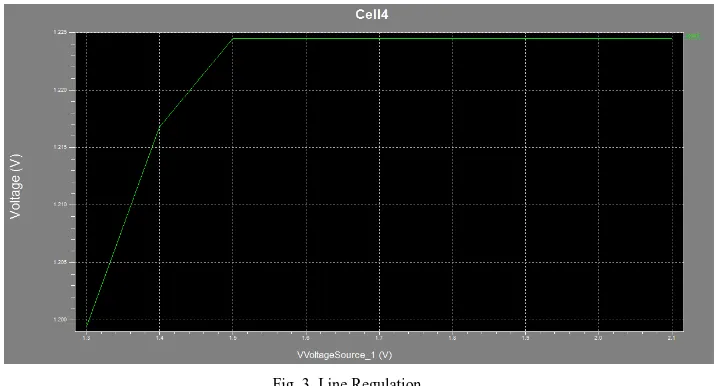
The output voltage of the proposed LDO voltage regulator with the input voltage swept from 1.3 V to 2.1V is given in figure 3.
Fig. 3. Line Regulation
Fig. 4. Load Regulation
The simulation result illustrates that the output voltage variation is 933μV with the load current changing from 0 to 1 mA, resulting in the load regulation of 933μV/mA.
C. Dynamic-state regulation characteristics
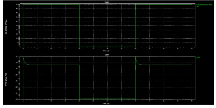
The load transient response of the proposed LDO voltage regulator with 100fF on-chip output capacitor is given by figure 5. Figure 5(a) shows the input waveform, figure 5(b) shows the output waveform for rising edge, figure 5(c) shows the output waveform for falling edge. The load current varies between 1mA and 50mA with rising and falling
time of 1μs.
(b)
(c)
Fig. 5. Load transient response
The simulation results illustrate that the output voltage variatio n is 11.98mV, 87uV respectively, with settling time of 1.77μs, 0.285us.
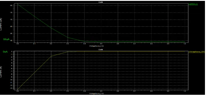
Fig. 6 presents the quiescent current IQ against the output current. Simulated result illustrate that the LDO regulator consumes 91 μA current.
E. Summarized characteristics and comparisons
The characteristics of the proposed LDO voltage regulator is summarized in Table 1, and compared with references [1], [5], [6], [10] and [11].
Table1. Comparison of the proposed LDO regulator with other LDOs
Parameters [1] [5] [6] [10] [11] This work
Year 2011 2014 2014 2015 2014 2015
Technology 180nm 65 nm 65 nm 180 nm 130 nm IBM 90 nm
Iload(max) 150 mA 50 mA 50 mA 50 mA 5 mA 50 mA
Iload(min) - 0.01 mA 0 - 5mA
Vin(min) 3.3 V 1 V .75-1.2V 1.8 V 1.2 V 1 V
Vout(max) 1.8 V - 0.5V 1.6 V 1 V 0.9V
Vdrop 1.5V - 0.7V 0.2 V 0.2 V 0.1V
Load Capacitor(CL) - - 0-100 pF 20 pF .1pF,1pF, 7pF
Quiescent Current (IQ) 90 μA 27.5 μA 16.2 μA 80 μA 99.04 μA 90 μA
ΔVout 155 mV 17.5 or 11 mV 103 mV 103 mV 50 mV <12mV
ΔIload - - 50 mA - 45mA
Setlling time 1.4 μs - 1.2 μs - 0.16 μs 1.77μs/.28μs
Line Regulation 13.75 μV/mV 4 mV/V - - 41mV/V
PSR (dB)
@ 1 KHz - -46 dB -46 dB - -93.6 dB -34.3 dB
@ 1 MHz -10 dB -35 dB -4 dB -52 dB -57.11 dB -43.6 dB
@ 10 MHz - - - -29 dB -41.15 dB -50 dB
Edge Time - 200 ns 100 ns - 5 ns
FOM - 12.1 fs 33.4 mV 0.000066 ns 43.2 as
From above table we have analysed that bulk voltage of 500mV is good choice to obtain the high PSRR at 90-nm technology and at variable load capacitor and load current.
VI. CONCLUSION
A low drop out voltage regulator has been designed on 90 nm and simulated in Tanner EDA software. To improve the performance of LDO voltage regulator, threshold voltage of pass transistor has been modulated by varying substrate voltage of 200 mV, which regulates the output voltage at 0.9 V from 1 V supply with minimum drop-out voltage of 100 mV and delivering maximum output current of 50 mA. The use of this technique allows us to achieve high PSRR, which has found out to be 50 dB at 10 MHz and low FOM of 43.2 as. Within the scope of power management system low quiescent current consumption is required which is 90 μA and ΔVout is less than 12 mV.
REFERENCES
[1] Lv Xiaopeng, Bian Qiang, Yue Suge, “An on-chip Low Drop-Out Voltage Regulator with 150mA Driving Capability,” World Congress on Engineering and Computer Science, Vol II, 2011.
[2] Herminio Martínez-García, “Design of a 4.5-V, 450-mA Low-Dropout Voltage Linear Regulator Based on a Cascoded OTA,” SAAEI, pp.654-659,2012.
[3] Leo C. J., Raja M. K. and Je Minkyu, “An ultra low-power capacitor-less LDO with high PSR,” IEEE MTT-S International Microwave Workshop Series on RF and Wireless Technologies for Biomedical and Healthcare Applications (IMWS-BIO), 2013.
[4] Cheekala Lovaraju, Ashis Maity and Amit Patra, “A Capacitor-less Low Drop-out (LDO) Regulator with Improved Transient Response for System-on-Chip Applications,” 26th International Conference on VLSI Design and the 12th International Conference on Embedded Systems, pp.130-135, 2013.
[5] Fan Yang and Philip K.T. Mok, “Area-Efficient Capacitor-less LDR with Enhanced Transient Response for SoC in 65-nm CMOS,” IEEE pp.2325-2328, 2014.
[6] Sau Siong Chong and Pak Kwong Chan, “A Sub-1 V Transient-Enhanced Output-Capacitorless LDO Regulator With Push–Pull Composite Power Transistor” IEEE transaction on very large scale integration (VLSI) system, pp.1-10,2014.
[7] Sreehari Rao Patri, Suresh Alapati , Surendra Chowdary and Krishna Prasad “250mA Ultra Low Drop Out Regulator With High Slew Rate Double Recycling Folded Cascode Error Amplifier,” IEEE 2014.
[8] Longjie Du, Yizhong Yang, Yang Chen, Guangjun Xie, and Xin Cheng, “An Ultra Low Quiescent Current CMOS Low-Dropout Regulator with Small Output Voltage Variations,”Journal of Power and Energy Engineering, pp.477-482, 2014.
[9] Chang-Joon Park, Jose Silva-Martinez and Marvin Onabajo “Design Techniques for External Capacitor-less LDOs with High PSR over Wide Frequency Range,” IEEE, pp.342-345, 2014.
[10] Seong Jin Yun, Jeong Seok Kim, Taikyeong Ted. Jeong and Yong Sin Kim “A Capacitor-less Low Dropout Regulator for Enhanced Power Supply Rejection,” IEEE Transaction on Smart Processing and Computing, vol 4, no. 3, pp.152-157, 2015.