ISSN(Online): 2320-9801
ISSN (Print): 2320-9798
I
nternational
J
ournal of
I
nnovative
R
esearch in
C
omputer
and
C
ommunication
E
ngineering
(An ISO 3297: 2007 Certified Organization)
Vol. 3, Issue 5, May 2015
Design of an Area Efficient Adder Using
Minority Gates in QCA
Abilash.B
1,
Kirubakaran.T
2,
Ishwarya Niranjana.M
3PG Student, Sri Shakthi Institute of Engineering and Technology, Coimbatore, India1
Assistant Professor, Sri Shakthi Institute of Engineering and Technology, Coimbatore, India2
PG Student, Sri Shakthi Institute of Engineering and Technology, Coimbatore, India3
ABSTRACT: The area and complexity are the major issues in circuit design. As transistors decrease in size more and more of them can be accommodated in a single die, thus increasing chip computational capabilities. However, transistors cannot get much smaller than their current size. The Quantum-dot Cellular Automata (QCA) approach represents one of the possible solutions in overcoming this physical limit. Here a Ripple Carry Adder (RCA) module is proposed that can serve as a basic component for QCA arithmetic circuits. The main methodological design innovation over existing state of the art solutions was the adoption of so called minority gates in addition to the more traditional majority voters. The proposed adder is designed and simulated using QCA designer 2.0.2. Simulation results show that the proposed adder outperforms all state of-the art competitors and reduces area-delay efficiently than previous designs.
KEYWORDS: Quantum-dot Cellular Automata(QCA), Multiplexer, Logic Gates.
I. INTRODUCTION
Quantum-dot Cellular Automata (QCA) is an efficient technology to create computing devices. QCA is a suitable candidate for the next generation of digital systems. A quantum-dot cellular automaton (QCA) is a new nanotechnology that can help us to reach low-power consumption, high device density, and high clock frequency. QCA size is smaller than CMOS it can, even be implemented in molecule or atom size. QCA power consumption is extremely lower than CMOS because there are not any current in the circuit and output capacity.
In recent years CMOS technology demonstrated that it can be readily challenged by other technologies when it arrives at nano-regimes. Due to serious CMOS technology restrictions in nano -scales, researchers have investigated alternative technologies [2]. As the electronic CMOS transistor technology for information processing approaches its limits, new possibilities for the implementation of digital information processing are being explored. Among those raising greatest interest are Quantum Cellular Automata (QCA). QCA are matrixes of cells, in which information is stored as the position of couples of electrons bound within cell borders. Neighbour cells interact by means of electric Columbian repulsion, and cell state can be frozen at will by controlling a potential barrier rising signal (clock). Quantum Cellular Automata (QCA) refers to models of quantum computation, which have been devised in analogy to
conventional models of cellular automata introduced by von Neumann
.
It may also refer to quantum dot cellular automata, which is a proposed physical implementation of "classical" cellular automata by exploiting quantum mechanical phenomena. QCA has attracted a lot of attention as a result of its extremely small feature size (at the molecular or even atomic scale) and its ultra-low power consumption, making it one candidate for replacing CMOS technology.
II. RELATED WORK
ISSN(Online): 2320-9801
ISSN (Print): 2320-9798
I
nternational
J
ournal of
I
nnovative
R
esearch in
C
omputer
and
C
ommunication
E
ngineering
(An ISO 3297: 2007 Certified Organization)
Vol. 3, Issue 5, May 2015
Fig.1 A simplified diagram of a four-dot QCAcell.
Fig.1 shows a simplified diagram of a quantum-dot cell. If the cell is charged with two electrons, each free to tunnel to any site in the cell, these electrons will try to occupy the furthest possible site with respect to each other due to mutual electrostatic repulsion. Therefore, two distinguishable cell states exist. shows the two possible minimum energy states of a quantum-dot cell. The state of a cell is called its polarization, denoted as P. Although arbitrarily chosen, using cell polarization P = -1 to represent logic ―0‖ and P = +1 to represent logic ―1‖ has become standard practice [2].
Grid arrangements of quantum-dot cells behave in ways that allow for computation. The simplest practical cell arrangement is given by placing quantum-dot cells in series, to the side of each other. Figure 4 shows such an arrangement of four quantum-dot cells. The bounding boxes in the figure do not represent physical implementation, but are shown as means to identify individual cells. If the polarization of any of the cells in the arrangement shown in Fig.3 were to be changed (by a "driver cell"), the rest of the cells would immediately synchronize to the new polarization due to Columbic interactions between them. In this way, a "wire" of quantum-dot cells can be made that transmits polarization state. Configurations of such wires can form a complete set of logic gates for computation.
III.PROPOSED METHOD
A. MAJORITY GATES:
QCA Majority Gate Perhaps the most important logic gate in QCA is the majority gate. Fig.4 shows a majority gate with three inputs and one output. In this structure, the electrical field effect of each input on the output is identical and additive, with the result that whichever input state ("binary 0" or "binary 1") is in the majority becomes the state of the output cell — hence the gate's name. For example, if inputs A and B exist in a ―binary 0‖ state and input C exists in a ―binary 1‖ state, the output will exist in a ―binary 0‖ state since the combined electrical field effect of inputs A and B together is greater than that of input C alone [3].
ISSN(Online): 2320-9801
ISSN (Print): 2320-9798
I
nternational
J
ournal of
I
nnovative
R
esearch in
C
omputer
and
C
ommunication
E
ngineering
(An ISO 3297: 2007 Certified Organization)
Vol. 3, Issue 5, May 2015
B. LOGIC GATES:
Logic gates, namely AND gates and OR gates, can be constructed using a majority gate with fixed polarization on one of its inputs. A NOT gate, on the other hand, is fundamentally different from the majority gate. The key to this design is that the input is split and both resulting inputs impinge obliquely on the output. In contrast with an
orthogonal placement, the electric field effect of this input structure forces a reversal of polarization in the output.
C. INVERTER:
Fig.3 Standard Implementation of a NOT gate.
Logic gates, namely AND gates and OR gates, can be constructed using a majority gate with fixed polarization
on one of its inputs. A NOT gate, on the other hand, is fundamentally different from the majority gate.The key to
this design is that the input is split and both resulting inputs impinge obliquely on the output. In contrast with an
orthogonal placement, the electric field effect of this input structure forces a reversal of polarization in the output
.
D. AND AND OR GATE:
When one input C is fixed as logic ―0‖ then it act as AND gate and if C is logic ―1‖ then it act as OR gate.
The majority gate performs a three-input logic function. Assuming the inputs is A, B and C, the logic function of the majority gate is given as in (1)
M (A, B, C) = A.B + B .C + A.C (1)
By fixing the polarization of one input to the QCA majority gate as logic ―1‖ or logic ―0,‖ an AND gate or OR gate will be obtained.
M(A,B,0) = AB (2)
M(A,B,1) = A+B (3)
E. XOR GATE:
Digital circuits can be implemented by using basic logic gates like AND, OR and NOT, also universal gates NAND and NOR can be used. In addition of these gates Exclusive-OR (XOR) and Exclusive-NOR (XNOR) are also used. To design any arithmetic circuit and complex circuit XOR and XNOR gates are useful, since these gate are complex to fabricate with hardware usually ground as two input gates [9]. An XOR gate can be trivially constructed from the basic gate AND, OR and NOT gates. The XOR function performs the following logic operation. The operational function of XOR gate can be represented as in (4)
ISSN(Online): 2320-9801
ISSN (Print): 2320-9798
I
nternational
J
ournal of
I
nnovative
R
esearch in
C
omputer
and
C
ommunication
E
ngineering
(An ISO 3297: 2007 Certified Organization)
Vol. 3, Issue 5, May 2015
F.CLOCKS:
Each QCA cell spends four states during a clock cycle as shown in Fig.7. QCA cell states are named as switch and hold and release and relax states. During the switch phase, QCA cells begin unpolarised and their inter-dot potential barriers are low. The barriers are then raised during this phase and the QCA cells become polarized according to the state of their driver (i.e. their input cell). It is in this clock phase that the actual computation (or switching) occurs. By the end of this clock phase, barriers are high enough to suppress any electron tunnelling and cell states are fixed. During the hold phase, barriers are held high so the outputs of the sub array can be used as inputs to the next stage. In the release phase, barriers are lowered and cells are allowed to relax to an unpolarised state.
Fig.4 Four Phases of Clock
Finally, during the fourth clock phase, the relax phase, cell barriers remain lowered and cells remain in an unpolarised state. As we know, the clock signals coming periodically from the clock source and so four clock phases’ signals are activated periodically and in each clock phase, a part or sub circuit of a circuit is activated periodically in its clock phase. When we place some QCA cell in a clock phase such as phase0, then these cells go to switch state when the phase1 signal is being activated. QCA cell has not any polarity and can’t be affected by neighbour cells.
In switch state, a QCA cell could take a logic 0 or 1 polarization from the input cells or its neighbor cells. at the end of switch state ,the next clock phase signal is coming and the QCA cell go to the hold state and those QCA cells which are placed in the next clock phase(phase1) go to the switch state and can be affected by those cells which are placed in the previous clock phase. A QCA cell that is in the hold state, hold its polarity and after a clock phase by coming the next clock phase signal, it comes into the release state. In the release state, the QCA cell releases its polarity and can’t be affected by the input signals or neighbor cells. In the next clock phase the QCA cell go to the relax state. In the relax state the
G. MULTIPLEXER:
Multiplexers have a considerable role in the digital systems which allow to select one of the input’s flows for transmitting to the output. Whereas all the logic functions can be built by multiplexers, implementation of multi-input multiplexer in the one layer is a remarkable subject. The main building block of QCA circuits is majority gate and consequently the other logic circuits are implemented based on majority gate networks. To propose a novel designing approach to implement QCA logic circuits with least hardware overhead, in addition to three-input majority gate, five-input majority gate is employed . In this approach, some functional logic circuits are implemented by configuration of five-input majority gate inputs.
As shown in Fig.11, X, Y, Z are labelled as the main inputs and the control input is labelled as control line. In addition, one of these inputs has twice the effect of the other inputs on five-input majority gate. By setting control line to ―1‖ logic value, the Boolean function X+YZ is obtained. Furthermore, logical function X(Y+Z) can be achieved by changing the value of the control line to ―0‖.
By using the five-input majority function, we get the following equations:
ISSN(Online): 2320-9801
ISSN (Print): 2320-9798
I
nternational
J
ournal of
I
nnovative
R
esearch in
C
omputer
and
C
ommunication
E
ngineering
(An ISO 3297: 2007 Certified Organization)
Vol. 3, Issue 5, May 2015
M5(Y, X, X, Z, 1) = YX+YXZ+YX+YX+YX+YZ+XZ+X+XZ+ XZ
=X+YZ (6)
Fig.5 Achieved Boolean expressions based on theproposed method.
It is worth mentioning that these functions need only one five-input majority gate for implementation. However, these functions are designed with two three-input majority gates in the conventional method. As noted above, a feasible design for 2-to-1 multiplexer can be obtained by utilizing the proposed novel method. According to the 2-to-1 multiplexer function, the inputs of logical function X+YZ should be changed as Fig.12(a) .The logic function B.S should be fed to input X and also the input A and should be fed to the input Y and Z, respectively. For implementation of logical function BS, a three-input majority gate has been used. It is to be noted that only two majority gates and one inverter gate are used for implementing this structure.
Fig.6 (a) Schematic of the proposed 2-to-1multiplexer based on new approach,
(c) QCA implementation of 2-to-1 multiplexer.
By applying this method, the equation of 2-to-1 multiplexer is defined as follows:
M5(A,M3(B,0,S) , M3(B,0,S) , S ,1) (7)
M5(A, BS , BS, S ,1) = A S + BS (8)
ISSN(Online): 2320-9801
ISSN (Print): 2320-9798
I
nternational
J
ournal of
I
nnovative
R
esearch in
C
omputer
and
C
ommunication
E
ngineering
(An ISO 3297: 2007 Certified Organization)
Vol. 3, Issue 5, May 2015
IV.FUNCTIONALITY OF PROPOSED CIRCUIT
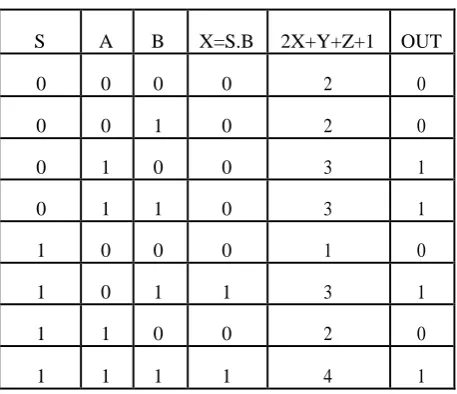
Table 1
Truth table of functionality of proposed circuit
As it is obvious in Fig. 12(b), the latency of proposed multiplexer is 0.75 clock cycle, so this design is the fastest in comparison to previous mentioned designs.
V. SIMULATION RESULTS
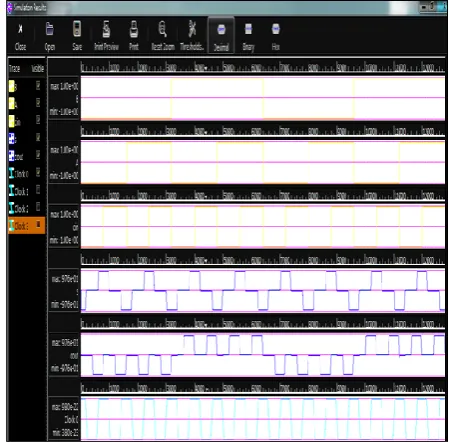
Basic Module is designed using minority gates. The most significant carry will be ready after 2/4 of a clock period after the beginning of the computation, while both the sum signals are ready in a single clock cycle. In fact, increasing of one bit the capacity of the adder leads to an increment of its latency of only 1/4 of clock cycle, both for the CarryOut and the for the Sum signals. In 4 bit adder, its design structure and its latencies can be connected modularly without requiring any clock regions re-phase, and it is then very suitable for the implementation of higher order adders such as 8, 16, 32 and 64 bit adders.
The proposed adder (64-bit) layout design as shown in Figure 4.7 outperforms all state-of-the art competitors and reduces area-delay efficiently than previous designs. The adder designed is expected to span over a complexity of
15939 (cell count) and 15.32 μm2 of active area in 33 clock phases.
Figure 4.2 shows the Basic Module of Ripple Carry Adder designed based on the concept of minority gates and its simulation result is checked as per truth table of Full Adder. The Carry and Sum is generated and checked for each case.
S A B X=S.B 2X+Y+Z+1 OUT
0 0 0 0 2 0
0 0 1 0 2 0
0 1 0 0 3 1
0 1 1 0 3 1
1 0 0 0 1 0
1 0 1 1 3 1
1 1 0 0 2 0
ISSN(Online): 2320-9801
ISSN (Print): 2320-9798
I
nternational
J
ournal of
I
nnovative
R
esearch in
C
omputer
and
C
ommunication
E
ngineering
(An ISO 3297: 2007 Certified Organization)
Vol. 3, Issue 5, May 2015
Fig: 7 Basic Module And Its Simulation Result Fig :8 Basic Module and simulation result
Fig: 9 32-bit adder and simulation results
ISSN(Online): 2320-9801
ISSN (Print): 2320-9798
I
nternational
J
ournal of
I
nnovative
R
esearch in
C
omputer
and
C
ommunication
E
ngineering
(An ISO 3297: 2007 Certified Organization)
Vol. 3, Issue 5, May 2015
VI.CONCLUSION AND FUTURE WORK
The optimized design of Ripple Carry adder is proposed. The proposed Adder is simulated using QCA designer tool 2.0.2 Version and is efficient in terms of cell count and area. The proposed work has shown that it is possible to significantly reduce the number of cells required to design basic components, such as adder circuits, by utilizing minority gates instead of majority gates. In addition to this, the proposed design presents an increased robustness with respect to previous approaches. The Proposed adder (64-bit) spans over a complexity of 15939 (cell count) covering 15.32 μm2 of active area and shows a delay of only 81/4 clock cycles, that is just 33 clock phases.
An interesting extension of the proposed work could be the automation of the optimizations in order to make it possible to synthesize more complex circuits. The cell count can further be reduced by using 5, 7, 9 input Majority Gates.
REFERENCES
.
[1] Stefania Perri, Pasquale Corsonello and Giuseppe Cocorullo,‖Area-Delay Efficient Binary Adders in QCA‖,IEEE Trans. On Very Large Scale Integeratio(VLSI) Systems,vol.22.no.5,May 2014.
[2] M.Mustafa and M.R.Beigh, ―Design and implementation of Quantum Cellular Automata based novel Parity generator and checker circuits with minimum complexity and cell count‖, Indian Journal of Pure & Applied Physics, vol. 451, pp. 60–60, Jan. 2013.
[3] Francesco Bruschi, Francesco Perini,Vincenzo Rana and Donatella Sciuto ,― An Efficient Quantum-Dot Cellular Automata Adder‖,978-3-9810801-7-9/DATE11/@2011 EDAA.
[4] Sen. Wang, Li. Cai, Novel exclusive-OR gate and full adder implementation using quantum cellular automata, Solid-state phenomenon. 565– 569, 2007.
[5] Heumpil Cho et al. Adder and multiplier design in quantum-dot cellular automata. IEEE Transactions on Computers, 58(6):721–727, 2009. [6] Kim Kyosun et al. Towards designing robust qca architectures in the presence of sneak noise paths. In DATE ’05, pages 1214–1219, Washington, DC, USA, 2005. IEEE Computer Society.
[7] C. Bencher, Y. Chen, H. Dai, W. Montgomery, and L. Huli, ―22nm half-pitch patterning by CVD spacer self alignment double patterning (SADP),‖ Proc.SPIE, vol. 6924, p. 69244E, Mar. 2008.
BIOGRAPHY
Abilash.B is a PG Student (VLSI design) in Sri Shakthi Institute of Engineering and Technology, Coimbatore. He has his Bachelor’s degree (ECE) from Tamilnadu College of Engineering, Coimbatore. He has undergone six month
internship at Intel Technology India Pvt. Ltd., Bangalore during the second year of his PG course. His areas of