International Journal of Research (IJR)
e-ISSN: 2348-6848, p- ISSN: 2348-795X Volume 2, Issue 12, December 2015Available at http://internationaljournalofresearch.org
Adaptive Test Pattern Generation Using BIST Schemes
Manthapuri Shirisha & G.Vedhavathi
*M.TECH ,Dept of ECE, Vaagdevi Engineering College Warangal [email protected]
**Assistant. Prof Dept of ECE, Vaagdevi Engineering College Warangal
ABSTRACT
A Test Pattern Generator (TPG) is used for generating different test patterns in Built-In Self-Test (BIST) schemes. This work generates Multiple Single Input Change (MSIC) vectors in a pattern, applies each vector to a scan chain is an SIC vector. A MSIC-TPG and Accumulator based TPG are designed and developed a reconfigurable Johnson counter and a scalable SIC counter to generate a class of minimum transition sequences. The Test Pattern Generator is flexible to both the test-per-clock and the tester-scan schemes. A theory is also developed to represent and analyze the sequences and to extract a class of MSIC sequences. Analysis results show that the produced Multiple Single Input Change sequences have the favorable features of uniform distribution and low input transition density. It also achieves the target fault coverage without increasing the test length. The architecture modifies scan-path structures, and let the Circuit Under Test (CUT) inputs remain unchanged during a shift operation. Compared with the MSIC-TPG, the proposed Accumulator based TPG achieves reduced area and average power consumption during scan based tests and the peak power in the CUT. By writing VHDL coding, the test patterns are simulated using MODELSIM and the results are validated.
I.INTRODUCTION
BIST is a design-for-testability technique that places the testing functions physically with the circuit under test (CUT). The basic BIST architecture requires the addition of three hardware blocks to a digital circuit: a test pattern generator, a response analyzer, and a test controller. The
test pattern generator generates the test patterns for the CUT. Examples of pattern generators are a ROM with stored patterns, a counter, and a linear feedback shift register (LFSR). A typical response analyzer is a comparator with stored responses or an LFSR used as a signature analyzer. It compacts and analyzes the test responses to determine correctness of the CUT. A test control block is necessary to activate the test and analyze the responses.
International Journal of Research (IJR)
e-ISSN: 2348-6848, p- ISSN: 2348-795X Volume 2, Issue 12, December 2015Available at http://internationaljournalofresearch.org
simulation at a place on the chip (like ROM). An n input circuit would then require 2^n combinations which can be very tiresome on the system with respect to the space and the time. Also, more the number of transitions, the power consumed will be more. A Novel low-transition Linear Feedback Shift Register (LFSR) [1] that is based on some new observations about the output sequence of a conventional LFSR. The proposed design, called Bit-Swapping LFSR composed of a LFSR and a 2 × 1 multiplexer. The Bit-Swapping LFSR is combined with a scan-chain-ordering algorithm that orders the cells in a way that reduces the average and peak power in the test cycle or while scanning out a response to a signature analyzer.
These techniques have a substantial effect
on average- and peak-power reductions with negligible effect on fault coverage or test application time. A new weighted random pattern design for estability is described where the shift register latches distributed throughout the chip are modified so that they can generate biased pseudo-random patterns upon demand. A two-bit code is transmitted to each weighted random pattern shift register latches to determine its specific weight. The weighted random pattern test is then divided into groups, where each group is activated with a different set of weights. The weights are dynamically adjusted during the course of the test to "go after" the remaining untested faults. An
accumulator-based 3- weight test pattern
generation scheme is presented; the proposed scheme generates set of patterns with weights 0, 0.5, and 1. Since accumulators are commonly found in current VLSI chips, this scheme can be efficiently utilized to drive down the hardware of built in self test pattern generation, as well. Comparisons with previously presented schemes indicate that the proposed scheme compares favorably with respect to the required hardware .A
new design methodology for a pattern generator, formulated in the context of on-chip BIST.
The design methodology is circuit-specific and uses synthesis techniques to design BIST generators [15]. The pattern generator consists of
two components: a pseudorandom pattern
generator like an LFSR and a combinational logic to map the outputs of the pseudorandom pattern generator. This combinational logic is synthesized to produce a given set of target patterns by mapping the outputs of the pseudorandom pattern generator. An improved scan-based BIST scheme which achieves very high fault coverage without any modification of the mission logic [12], i.e. No test point insertion, no test data to store and very simple BIST hardware which does not depend on the size of the circuit.
II. RELATED WORK
A new Low Power Test Pattern Generator using a Linear Feedback Shift Register called LP-TPG It is used to reduce the average and peak power of a circuit during test [2]. The correlation between the test patterns generated by LP-TPG is more than conventional LFSR. LP-TPG inserts
Intermediate patterns between the random patterns. A Built in Self Test for low power dissipation and high fault coverage presents a low hardware overhead test pattern generator for scan-based Built-In Self-Test that can reduce switching activity in Circuits under Test during BIST and also achieve very high fault coverage with reasonable lengths of test sequences. The BIST TPG comprises of two TPG's, Low Transition TPG and 3- weight BIST [3].
International Journal of Research (IJR)
e-ISSN: 2348-6848, p- ISSN: 2348-795X Volume 2, Issue 12, December 2015Available at http://internationaljournalofresearch.org
Feedback Shift Register capable of generating a given finite sequence. On the BIST design stage and considering the fault-free test response sequence, the BMA is used to synthesize an LFSR capable of generating this sequence in an economical way. A testing for the interesting Built-in Self-Test technique [5] for the mBuilt-inimal number of test patterns .It requires predefined fault coverage. The technique is not applicable for the existing deterministic test pattern generators. It has enormous consumers of overhead silicon area. A new low power BIST test pattern generator that provides test vectors which can reduce the switching activity during test operation [6]. It has been implemented based on an LFSR-based TPG, but can also be designed using a cellular automata. A new BIST TPG design that is comprised of an Adjacency-based TPG plus a conventional pseudo-random TPG [7] (i.e. a LFSR).When used to generate test patterns for test-per-clock BIST, it reduced the number of transitions that occur in the CUT and hence decreases the average and peak power consumption during testing. Low ower consumption during scan-based testing [9]. The testing process has two modes they are shift and capture modes. The circuit reliability is high during manufacturing test. The work proposed a novel X-filling technique, namely “infill”, to address the above issue, by analyzing the impact of X-bits on switching activities of the circuit nodes in the two different phases. In addition, different from prior X-filling methods for shift-power reduction that can only reduce shift-in power. The BIST techniques based on reseeding of multiple-polynomial linear feedback shift registers [8]. This scheme encodes deterministic test sets at distinctly lower costs than previously known approaches. In this work it is shown how this scheme can be supported during test pattern generation. The
presented ATPG algorithm generates test sets which can be encoded very efficiently.
The Built-in Test Pattern Generation mechanisms that can enforce a prescribed exact set of phase shifts, or channel separations [10].The bit sequences produced by their successive stages, while still requiring low hardware overhead. A new technique which maintains the benefits of
mixed-mode Built-In Self-Test (low test
application time and high fault coverage) [17], and reduces the excessive power dissipation associated with scan-based test. A delay fault detection Built-In-Self-Test. An adjacency test pattern generation scheme can generate robust test patterns effectively [14]. A pseudo-functional BIST scheme that attempts to minimize the over-testing problem of logic BIST for delay and crosstalk-induced failures [20]. A new Adaptive Low Shift Power Random Test Pattern Generator (ALP-RTPG) [19] to improve the tradeoff between test coverage loss and shift power reduction in logic BIST. This is achieved by applying the information derived from test responses to dynamically adjust the correlation among adjacent test stimulus bits.
III. EXISTING SYSTEM 3.1 MSIC-TPG
International Journal of Research (IJR)
e-ISSN: 2348-6848, p- ISSN: 2348-795X Volume 2, Issue 12, December 2015Available at http://internationaljournalofresearch.org
The generated code word is XORed with the same vector. The test pattern with the test vector will be applied to the scan chains. The MSIC-TPG consists of SIC generator, seed generator, XOR gate network, clock, and control Block.
3.2 SIC GENERATOR
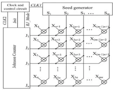
There are several types of SIC generator. Out of this, one type of SIC generator is the Johnson vectors, that are generated by the reconfigurable Johnson counter as shown in fig.3.1
Fig. 3.1 Reconfigurable Johnson Counter
Reconfigurable Johnson Counter can operate in three modes.
Initialization: When RJ_Mode is set to 1 and Init is set to logic 0, the reconfigurable Johnson counter will be initialized to all zero states by clocking CLK2 more than l time.
Circular shift register mode: When RJ_Mode and Init are set to logic 1, each stage of the Johnson ounter will output a Johnson codeword by clocking CLK2 L-times.
Normal mode: When RJ_Mode is set to logic 0, the reconfigurable Johnson counter will generate 2l unique SIC vectors by clocking CLK2 2L times.
MSIC-TPG FOR TEST-PER-CLOCK SCHEMES
Fig. 3.2 Test per clock
The MSIC-TPG for test-per-clock schemes is illustrated in the fig.3.2. The CUT’s PIs X1 – X mn are arranged as an n ×m SRAM-like grid structure. Each grid has a two input XOR gate whose inputs are tapped from a seed output and an output of the Johnson counter. The outputs of the XOR gates are applied to the CUT’s PIs. A seed generator is an m-stage conventional LFSR, and operates at low frequency CLK1. The test procedure is as follows.
1) The seed generator generates a new seed by clocking CLK1 one time.
2) The Johnson counter generates a new vector by clocking CLK2 one time.
3) Repeat 2 until 2L Johnson vectors are generated. 4) Repeat 1–3 until the expected fault coverage or test length is achieved.
3.3 MSIC-TPG FOR TEST-PER SCAN
International Journal of Research (IJR)
e-ISSN: 2348-6848, p- ISSN: 2348-795X Volume 2, Issue 12, December 2015Available at http://internationaljournalofresearch.org
Fig. 3.3 Test per Scan
The MSIC-TPG for test-per-scan schemes is illustrated in fig 3.3 the stage of the SIC generator is the same as the maximum scan length, and the width of a seed generator is not smaller than the scan chain number.
The inputs of the XOR gates come from the seed generator and the SIC counter, and their outputs are applied to M scan chains, respectively. The outputs of the seed generator and XOR gates are applied to the CUT’s PIs, respectively. The test procedure is as follows.
the seed circuit generates a new seed by clocking CLK1 one time.
RJ Mode is set to “0”. The reconfigurable Johnson counter will operate in the Johnson counter mode and generate a Johnson vector by clocking CLK2 one time.
after a new Johnson vector is generated; RJ Mode and Init are set to 1. The reconfigurable ohnson counter operates as a circular shift register, and generates L code words by clocking CLK2 L time. Then, a capture operation is inserted.
Repeat 2–3 until 2L Johnson vectors are generated.
Repeat 1–4 until the expected fault coverage or test length is achieved.
The drawback of MSIC-TPG schemes having gating circuits, is that the circuits will possess high complexity. In the proposed system, Accumulator based TPG is used to overcome these problem. It is very simple to implement and this is very practical and has low complexity. Power consumption also decreases. The testing circuit area is also decreased.
IV. PROPOSED SYSTEM
4.1 ACCUMULATOR-BASED PATTERN GENERATION
New weighted random pattern designs for testability is described where the shift register latch is distributed throughout the chip are modified so that they can generate biased pseudo-random patterns upon demand. A two-bit code is transmitted to each weighted random pattern shift register latch to determine its specific weight. The weighted random pattern test is then divided into groups, where each group is activated with a different set of weights. The weights are dynamically adjusted during the course of the test to "go after" the remaining untested faults.
International Journal of Research (IJR)
e-ISSN: 2348-6848, p- ISSN: 2348-795X Volume 2, Issue 12, December 2015Available at http://internationaljournalofresearch.org
An accumulator-based 3-weight test pattern generation scheme is presented. The proposed scheme generates set of patterns with weights 0, 0.5, and 1. Since accumulators are commonly found in current VLSI chips, this scheme can be efficiently utilized to drive down the hardware of built in self test pattern generation, as well. Comparisons with previously presented schemes indicate that the proposed scheme compares favorably with respect to the required hardware. Accumulator architecture for proposed system is given in the Fig 4.1.
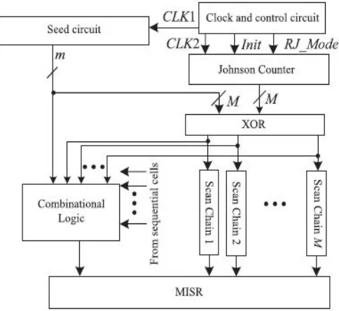
FAULT DETECTION
Inputs from the Johnson counter are given to the TPG as shown in Fig.4.2. The output of the TPG is given to the S344 (CUT). If the circuit has fault, it gives different patterns on the testing circuit and if the circuit is fault free, it gives same patterns on the testing circuit. Both fault and fault free circuits are analyzed using the analysis circuit.
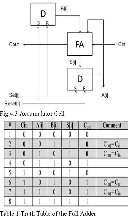
Fig.4.2 Block Diagram of Proposed System 4.2 3- WEIGHT PATTERN GENERATION The implementation of the weighted-pattern generation scheme is based on the full adder truth table, presented in Table 1. From Table 1, we can see that in lines #2, #3, #6, and #7 of the truth table, Cout = Cin. So, to transfer the carry input to the carry output, it is enough to set A[i] =NOT (B[i]). The proposed scheme is based on this observation.
The implementation of the proposed weighted pattern generation scheme is based on the accumulator cell presented. Figure 4.3 consists of a Full Adder (FA) cell and a D-type flip-flop with
asynchronous set and reset inputs whose output is also driven to one of the full adder inputs.
Fig 4.3 Accumulator Cell
Table 1 Truth Table of the Full Adder
In Figure 4.3, we assume, without loss of generality, that the set and reset are active high signals. In the same Figure 4.3, the respective cell of the driving register B[i] is also shown. For this accumulator cell, one out of two configurations can be utilized. Here we present this configuration that drives the CUT inputs.
International Journal of Research (IJR)
e-ISSN: 2348-6848, p- ISSN: 2348-795X Volume 2, Issue 12, December 2015Available at http://internationaljournalofresearch.org
2.For A[i] =0 , We give set[i]=0 and reset[i]=1 and hence A[i]=0 and B[i]=1. Then the output is equal to 0, and here Cin is equal to Cout. Cin is transferred to the Cout.
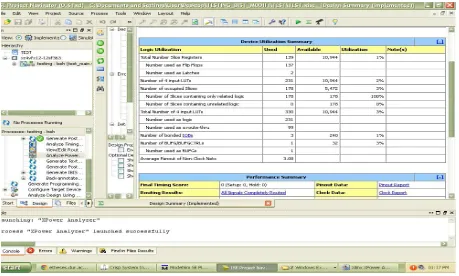
V. SIMULATION RESULTS
ModelSim is a simulation tool for hardware design which provides behavioural simulation of a number of languages, i.e., Verilog, VHDL, and System C. Verilog HDL is an industry standard language used to create analog, digital, and mixed-signal circuits. Verilog code is generated for this
accumulator circuit using 6.4c.Then RTL
schematic is produced using XILINK 13.2. These
test patterns are implemented in FPGA SPARTAN 3.
COMPARISON TABLE
Table 2 Comparison of Area and Power
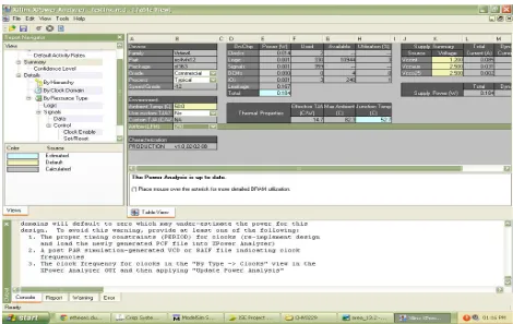
In this work area and power reduction is done by Xilinx ISE 13.2 version software. The MSIC-TPG technique produce area of 456m2 and for this, the corresponding power is 0.226w. Now the Accumulator based TPG technique produces reduced area of 139m2 and the corresponding power is reduced to 0.184w. The comparison results are tabulated in Table 2 and validated that The Accumulator based TPG has reduced area and power compared to MSIC-TPG. The output is shown in Fig 5.1 and Fig 5.2
International Journal of Research (IJR)
e-ISSN: 2348-6848, p- ISSN: 2348-795X Volume 2, Issue 12, December 2015Available at http://internationaljournalofresearch.org
Figure 5.2 Power analysis for Accumulator based TPG
VI. CONCLUSION AND FUTURE WORK Compared to the MSIC-TPG technique the Accumulator based 3-weight pattern generation technique has less fault coverage and lower hardware overhead. The hardware overhead of the proposed scheme is lower (75%). The testing time is also reduced to 20%–75%while at the same time no redesign of the accumulator is imposed. Finally, the accumulator based technique produces less Area and Power compared to the MSIC-TPG technique.
In the future, more refined methods for obtaining the controlled transition density mixing in the vector set, generated from LFSR by using linear programming approach is to be examined simultaneously to reduce the test time and test power more efficiently. The proposed system can be modified by the AND gate in case that the accumulator is implemented utilizing a carry-look ahead adder, or by a ripple carry adder in case the
accumulator is implemented for no delay applications as the future extension of the work.
REFERENCES
[1]. Abdallatif S. Abu-Issa and Steven F. Quigley “Bit-Swapping LFSR and Scan-Chain rdering: A Novel Technique for Peak- and Average- Power
Reduction in Scan-Based BIST”, IEEE
ransactions On Computer-Aided Design Of Integrated Circuits And Systems, Vol. 28, No. 5, May 2009.
[2]. Ahmed, N. ; Tehranipour, M.H. ; Nourani, M. “Low power pattern generation for BIST architecture “ IEEE International Symposium on Circuits and Systems, ISCAS '2004. Proceedings of the 2004 Print ISBN:0-7803-8251-X.
International Journal of Research (IJR)
e-ISSN: 2348-6848, p- ISSN: 2348-795X Volume 2, Issue 12, December 2015Available at http://internationaljournalofresearch.org
dissipation and high fault coverage” IEEE
International Conference on Computational
Intelligence and Computing Research (ICCIC), 2010 Print ISBN: 978-1-4244-5965- 0.
[4] Cleonilson Protásio de Souza and Francisco Marcos de Assis “A New Architecture of Test Response Analyzer Based on the Berlekamp– Massey Algorithm for BIST”, IEEE Transactions
On Instrumentation And Measurement, Vol. 59, No. 12, December 2010.
[5]. Dufaza, C. ; Viallon, H. ; Chevalier, C. “BIST hardware generator for mixed test scheme “ IEEE Proceedings on European Design and Test Conference, 1995. ED&TC 1995,. Print ISBN:0-8186-7039-8.
AUTHOR 1:-
*
M.SHIRISHA
Completed her B Tech in Prasad Engineering College and M-Tech in VAGDEVI ENGINEERING COLLEGE WARANGALAUTHOR 2:-
Miss. G.VEDHAVATHI
is working as Asst. prof in Dept of Ece Vagadevi Engineering College
WARANGAL with 4 years of Teaching Experience