Current Mode Control of a Series LC Converter
supporting Constant-Current Constant-Voltage
(CCCV)
Michael Heidinger1* , Qihao Xia1, Christoph Simon1, Fabian Denk1, Santiago Eizaguirre1, Rainer Kling1and Wolfgang Heering1
1 Karlsruhe Institute for Technology (KIT) - Light Technology Institute; Engesser Straße 13; 76131 Karlsruhe,
Germany
* Correspondence: [email protected]; Tel.: +49 721 608-47852
Abstract: This paper presents a control algorithm for soft-switching series LC converters. The conventional voltage-to-voltage controller is split into a master and a slave controller. The master controller implements constant-current-constant-voltage (CCCV) control, required for demanding applications, i.e. lithium battery charging or laboratory power supplies. It defines the set-current for the open-loop current slave controller, which generates the PWM parameters. The power supply achieves fast large-signal responses, e.g. from 5 V to 24 V, where 95% of the target value is reached in less than 400 µs. The design is evaluated extensively in simulation and on a prototype. A consensus between simulation and measurement is achieved.
Keywords: control; current mode control; voltage control; transfer function; power converter; soft-switching converter; battery charging;
1. Introduction
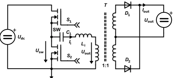
By the use of soft-switching converters high efficiency DC/DC converters can be built. One possible topology, a series LC (SLC) converter is shown in Figure1. The topology is similar to a series resonant converter, but it operates in a non-resonant push-pull mode [1]. In contrast to a dual active half bridge converter, the two secondary side active output switches are replaced with diodes [2].
A detailed time domain analysis for calculating the SLC output current, operated above the LC resonance frequency was published recently [1]. Current literature proposes a voltage-to-voltage transfer function [3]. We split the voltage-to-voltage converter in a cascaded structure [5]. A master controller sets the SLC output current, while a slave open-loop transfer function controls the switching period, duty cycle and pulse-skipping. The master voltage controller supports constant-current-constant-voltage (CCCV) operation, that is required e.g. for battery charging [6] or laboratory power supplies.
S
U S
L C Udc
T
out
1
i 1
2
SW
Iout D1
D2 Uout
1:1
Ii
Usw
Figure 1.The schematic of the series LC converter is identical to the series resonant converter, however the resonant capacitorC1is chosen large and acts as a DC blocking capacitor. The converter is operated far above its resonance frequency.
Equation (1) formulates the SLC converter output currentIccas a function of the input voltage
Udcand output voltageUoutbased on the control parameters duty cycleDand switching periodtp[1].
By adding pulse skipping, wherepoandpcrepresent the pulse skipping parameter defined in Figure
6, a very large output current range can be achieved.
Icc= po
pc
D(1−D)Udc2 −Uout2
4LiUdc
tp (1)
As the input voltage and also the output voltage are monitored in (1), this equation allows a very high rejection ratio [1]. The output voltage isUoutand the measured output voltage is referred
asUmeas. As large input voltage ripple can be rejected, this allows for a reduction of the DC link
capacitanceCdc. This enables the use of film capacitors instead of electrolytic capacitors, extending the
estimated service-life of the power supply.
The proposed control diagram is shown in Figure2. The control is based on four elements: {1}, the master voltage controller sets the current to the slave current controller. {2}, the slave current mode controller is an open-loop control transfer function, based on (1). The current controller sets four parameters to the PWM modulator {3}. The PWM modulator generates the PWM output waveform for the series LC converter {4}.
The controller is implemented on a digital signal processor (DSP), as (1) requires non-linear calculations. ADCs digitize the input voltage, output voltage and output current for the CCCV control. An MCU with integrated PWM module generates the switching signals for the half bridge.
Master Controller
Icc Slave
Controller
PWM Modulator
Series LC Converter {tp, D,
po, pc}
PWM
{Udc, Li} {Imax, Umax}
{tpp, Cout, UUadj , IIadj}
{Imeas, Umeas}
{Umeas}
{1} {2} {3} {4}
Figure 2.Proposed control diagram for the series LC converter. The converter is split into a master controller, implementing CCCV control, and an open-loop slave controller.
2. Master Voltage Mode Controller
The sensed currentIsenseshould be filtered to prevent systems oscillation when a capacitive load
is connected. In this design, a second order low pass filter with a cutoff frequency of 16 kHz is used. Both controllers are discussed in detail in the following subsections.
Uerr Umeas
Umax
UUadj
Ierr Imeas
Imax
IIadj
MIN
+
KiuKpu
Kii
+
-+
-Icc,CV
Kpi
Constant Voltage (CV) Controller
Constant Current (CC) Controller Filter
Isense
Ic
Icc
Icc,CC Ii
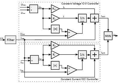
Figure 3. The master controller implements the CCCV functionality. The current and the voltage controllers operate in parallel and the smaller set value is selected for the output set currentIcc.
2.1. Constant Voltage Controller
The constant voltage controller limits the maximal output voltage toUmax. We design the voltage
control loop in Figure3based on circuit analysis of the output capacitorCout: The required set current
Icc,CVis expressed in (2). The filtered current is designatedImeas.
Icc,CV=Imeas+Ic+Ii (2)
The equalization current (Ic+Ii) is calculated by a PI regulator. The proportional gain is chosen on the
charge balance observation: We calculate the proportional equalizing currentIcas a function of the
output charge.
Q=Ic·tpp=Cout(Umax−Umeas) (3)
Ic= Cout
(Umax−Umeas)
tpp (4)
The time constanttppin (5) is chosen according to the maximal digital regulator control loop
period. Stability was observed by using a factor of 1/4 or less at a control loop frequency of 85.750 kHz. Hence the P regulator’s gain can be formulated as:
Kpu≤ Cout
4·tpp (5)
The DC voltage accuracy is enhanced by increasing the proportional gainKpu. Referring to (5),
An I regulator with reset is used to achieve stationary accuracy of the control. It adjusts a typically small error. To reduce overshoot, it is only activated if the error is lower than an absolute minimal error. We name this minimal voltageUUadj.
2.2. Constant Current Controller
The constant current controller limits the output current to Imax. Previous research already
demonstrated that the slave output current accuracyIccis better than 7% [1]. Therefore, the output
current is directly forwarded to the limiter. To compensate for inaccuracies, an additional PI regulator is used. If the absolute error is larger thanIIadj, the I regulator is reset to reduce overshoot for large
signal responses.
2.3. Acoustic Noise
When multi layer ceramic capacitors (MLCC) are used as output capacitors, they may emit acoustic noise due to the capacitors piezoelectric dielectric. If the master’s P gain is chosen close to the critical gain, noise is emitted. The acoustic noise is reduced by lowering the P gain or choosing low noise MLCCs.
Our experiments concluded that the following control loop gain eliminated the noise at the cost of a slightly slower step response.
Kpu≤ Cout
9·tpp (6)
3. Slave Current Controller
The slave current controller receives the set currentIccfrom the master controller. It is responsible
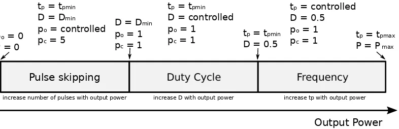
for selecting the appropriate modulation scheme: It chooses between adjusting the switching period, duty cycle or pulse skipping, as shown in Figure4.
Pulse skipping
Output Power tp = tpmin
D = Dmin
po = controlled
pc = 5
increase number of pulses with output power increase D with output power increase tp with output power
tp = controlled
D = 0.5 po = 1
pc = 1
tp = tpmin
D = controlled po = 1
pc = 1 t
p = tpmax
P = P max
po = 0
P = 0
D = Dmin
po = 1
pc= 1
tp = tpmin
D = 0.5
Figure 4.The slave current mode controller controls the frequency (fp=1/tp) for high output power, the duty cycle (D) for medium output power and pulse skipping (po/pc) for low output power. This modulation scheme maximises the output current range.
For adjusting the output power we propose the modulation strategy shown in Figure4. Pulse skipping is used for the lowest possible output power. The number of pulses may range between zero andpc. At medium output power, the duty cycle is increased fromD=DmintoD=0.5. At very high
output power, the switching period is increased until the maximal allowedtpmaxis reached.
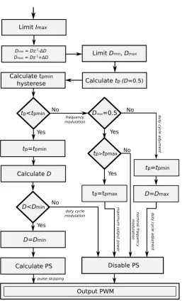
Calculate tpmin
hysterese
tp<tpmin
Calculate PS
D<Dmin
Calculate D tp=tpmin
D=Dmin
Output PWM
Disable PS
tp>tpmax
tp=tpmax No
No Yes
Yes
No
Yes
Calculate tp (D=0.5)
Limit Imax
Dmin = Dz-1-D
Dmax = Dz-1+
D
D=Dmax Yes
No frequency
modulation
duty c
ycle adjumen
t
tp=tpmin
maximum
output
power
nominal frequ
ency
modulation
duty c
ycle adjumen
t
duty cycle modulation
pulse skipping
Figure 5.Slave current mode controller algorithm
3.1. Initial Calculus
First, the minimal and maximal duty cycle are calculated, which are next limited. Second, the periodtpis determined using (7), which is based on (1), using a duty cycleD=0.5. Next, the minimum
periodtpminis calculated, which is a constant value, with an additional hysteresis. In the simulation
and experiments, no hysteresis was utilized. The maximum switching frequency is typically chosen in such a manner, that soft-switching of the half bridge can still be achieved.
tp= 16LiUdcIcc
Udc2 −4U2 meas
(7)
3.2. Frequency Modulation
If the periodtpis larger thantpmin, switching frequency modulation is used. To prevent the
unintentional false-triggering due to displacement current, the minimal periodtpminis used during
3.3. Duty Cycle Modulation
If the periodtpis smaller thantpmin, the duty cycle modulation is used. The duty cycle can be
determined by (1). As a quadratic equation has two results, one has to be chosen. To limit the voltage stress onC1, the smaller resulting duty cycle is used. This results to the following equation:
D=
Udctpmin−
q
Udc2 −4U2 meas
t2pmin−16IccLiUdctpmin
2Udctpmin (8)
3.4. Pulse Skipping
If the calculated duty cycle is smaller than the minimum duty cycleDmin, pulse skipping is used.
The pulse modulation is calculated according to the following formula, which can be converted to the on-pulse (po) and total number of periods (pc). An example for an PWM waveform with pulse
skipping is given in Figure6.
Icc= po
pc
Dmin(1−Dmin)Udc2 −Umeas2
4LiUdc
tp (9)
Currently, a fixed pulse skipping periodpcis used. However, also the Farey method could be used to
determine a more accurate ratio [4]. Ifpo<0.5, the PWM output is disabled. Thereby very low pulse
counts can be achieved.
3.5. Voltage Stress on C1
The voltageUcon the offset capacitorC1can be calculated using the following equation [1]:
Uc=DUdc (10)
To limit the voltage slope stress on the offset capacitorC1and slow down its aging, the duty cycle
is only changed slowly. Currently a value of∆D=0.02 per iteration is used to limit the stress on the DC blocking capacitorC1.
4. Modulator
The modulator generates the PWM waveform. It has four input parameters: The periodtp, the duty cycle D, the number of emitted pulsespo, and the number of pulses per periodpc. An example is
depicted in Figure6. The periodtp= fsw1 is the inverse of the switching frequency, and the duty cycle
states the ratio of the PWM high period. A switching cycle can be skipped by pulse skipping. The pulse skipping ontimepostates how many PWM pulses are emitted during a pulse skipping periodpc.
To prevent acoustic noise by pulse skipping, the pulse skipping frequency, should be larger than the maximal audible frequency fa=20 kHz:
1
pc tpmin
> fa (11)
5. Simulation and Experimental Results
The following section covers the simulation and measurement results for the CCCV converter.
5.1. Measurement Setup
To verify operation, the circuit is simulated with the software PLECS and tested in an experimental setup. The build converter prototype is shown in Figure7. The test parameters are shown in Table
1, unless otherwise noted. For the simulations and experiments, a load resistor ofRload =10Ωis
D t
p(1-D) t
pD t
p(1-D) t
pD t
p(1-D) t
pPWM
PWM waveform
issued
PWM waveform
issued
PWM waveform
not issued
t
p
op
cFigure 6.A PWM pulse skipping waveform is shown, where the period (tp), duty cycle (D), and pulse skipping ontime (po=2) and pulse skipping period (pc=3) are highlighted.
Figure 7.The prototype is mounted in a DIN rail case. It avoids electrolytic capacitors, and replaces them with film capacitors to achieve a longer service life.
Four tests are carried-out: {1}, a constant voltage step response test, {2} a constant current step response test, {3} a load response test and in {4}, the CCCV step response is verified. For each test setup, the corresponding output current and voltage are measured in the prototype. Additionally for each test pattern, output voltage and current are simulated as well. The depicted duty cycle and switching period are extracted from simulation only.
Table 1.Test setup parameters and conditions
Element/Parameter Value
Uin 325 V
Tratio 4.2:1
Li 110 µH
C1 470 nF
Cout 110 µF
Kpu 1.0
Kiu 857.5
UUadj 0.05Uset
Kpi 20
Kii 17150
IIadj 0.05Iset
∆D 0.02
Dmin,abs 0.2
tpmin 5 µs
pc 5
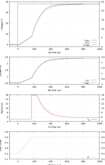
5.2. Voltage Step Response
The constant voltage controller limits the allowable output voltage. To verify the constant voltage controller, the maximal output voltageUmaxis increased in a step response att=0 from 5 V to 24 V
and the step response is shown in Figure8.
Before the step,t<0, the duty cycleDis limited atDmin=0.2. When the output power increases
aftert=0, the duty cycleDincreases each control loop iteration by steps of∆D=0.02 toD=0.5 for achieving maximum output power. After the duty cycle ramp-up, att≈180 µs, the switching period is limited to ensure over-resonant operation. When the set output voltageUmeasis about to reach the
maximal voltageUmax, the switching frequency is reduced.
In Figure8, the output voltage rises fast and reaches 95% of the target output voltage in less than 400 µs. A transition from pulse skipping at low load to switching frequency modulation at high load is demonstrated.
When the measured output voltage from the experimentUmeas is compared to the simulated
output voltageUsimin Figure8, a consensus is observed. The non-congruence betweent≈300 µs and
t≈600 µs arises due to non-linear MLCC capacitance.
5.3. Current Step Response
The constant current controller limits the maximum allowable output current. For the verification, the maximal output currentImaxis increased from 1 A to 2 A. The output current step response is
shown in Figure9. Beforet = 0, the converter operates in pulse skipping mode. Pulse skipping generates a significant ripple on the output voltage, as the effective switching frequency is very low.
Att= 0, the output currentImax is increased from 1 A to 2 A, and the duty cycle is increased fromD=0.2 toD=0.5 in increments of∆D=0.02, while using the minimal periodtpto prevent
over-current triggering. For charging the output capacitor Cout the slave controller first utilizes
frequency modulation, but switches att≈230 µs back to duty cycle modulation because the amount of required output power is reduced.
Current control reaches 95% of the output current target int ≈ 300 µs. Att < 400 µs the fine adjustment by the PI regulator is complete. The converter did not overshoot on the output current.
When the measured output current from the experiment Imeas is compared to the simulated
output current Isim in Figure9, a consensus can be observed. The slight difference is due to the
non-linear MLCC capacitance.
5.4. Load Response
The load response monitors the output voltage change while the load is increased. For this experiment, shown in Figure10, the output voltage is held constant atUmax=5 V while an external
current load is increased fromImeas=0.5 A toImeas=2 A att=0 . The output capacitor was chosen
in this experiment toCout=150 µF.
Before t < 0, the converter operates in pulse skipping mode, explaining significant output ripple. Att> 0 the output currentIoutincreases to 4 A. The duty cycle is increased by∆D=0.02
toD=0.5. Because of that, the converter cannot supply sufficient output power, hence the output voltage decreases. When the duty cycle adjustment is completed, at t ≈ 170 µs the duty cycle is constant atD=0.5, then the switching periodtpinstantly increases. An overshoot ofUos≈0.1 V is
observed in simulation. However, in the experiment this overshoot could not be measured. It must be denoted that the presented load jump represents the worst case.
5 10 15 20 25
0 200 400 600 800 1000 0
5 10 15 20 25
Voltage (V)
(a) time (µs)
Umax
Usim
Umeas
0.5 1 1.5 2 2.5
0 200 400 600 800 1000 0
0.5 1 1.5 2 2.5
Current (A)
(b) time (µs)
Isim
Imeas
4 6 8 10 12 14 16
0 200 400 600 800 1000 4
6 8 10 12 14 16
Period (µs)
(c) time (µs)
tp
0.1 0.2 0.3 0.4 0.5 0.6
0 200 400 600 800 1000 0.1
0.2 0.3 0.4 0.5 0.6
Duty Cycle
(d) time (µs)
D
0.8 1 1.2 1.4 1.6 1.8 2 2.2
0 200 400 600 800 1000 0.8
1 1.2 1.4 1.6 1.8 2 2.2
Current (A)
(a) time (µs)
Imax Isim
Imeas
8 10 12 14 16 18 20 22
0 200 400 600 800 1000 8
10 12 14 16 18 20 22
Voltage (V)
(b) time (µs)
Usim Umeas
5 6 7 8 9 10 11 12 13
0 200 400 600 800 1000 5
6 7 8 9 10 11 12 13
Period (µs)
(c) time (us)
tp
0.1 0.2 0.3 0.4 0.5 0.6
0 200 400 600 800 1000 0.1
0.2 0.3 0.4 0.5 0.6
Duty Cycle
(c) time (µs)
D
8 8.5 9 9.5 10 10.5 11
0 200 400 600 800 1000
Voltage (V)
(a) time (µs)
Umax Usim
Umeas
1 1.5 2 2.5 3 3.5 4
0 200 400 600 800 1000
Current (A)
(b) time (µs)
Isim
Imeas
5 5.2 5.4 5.6 5.8 6 6.2 6.4 6.6 6.8 7
0 200 400 600 800 1000
Period (µs)
(c) time (µs)
tp
0.1 0.2 0.3 0.4 0.5 0.6
0 200 400 600 800 1000
Duty Cycle
(d) time (µs)
D
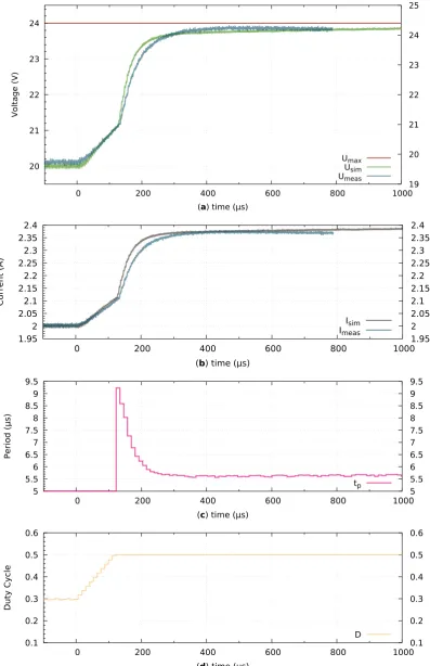
5.5. CCCV Transition Step Response
In Figure11, the constant current to constant voltage transition is measured. The effective output capacitance was determined to Cout = 45 µF. The converter is first operated in constant current
(CC) mode and then the transition to constant voltage (CV) is demonstrated. The CCCV control is implemented by choosing the minimal value of two parallel controllers, as it can be seen in Figure3. Att<0, the converter operates in CC mode and the output current is limited to 2 A. The load
Rload =10Ωresults in an output voltage ofUout=20 V. The voltage limit is set toUmax=24 V. After
t=0, the current limitImaxis increased from 2 A to 3 A. The output voltage rises from 20 V within
400 µs to the output voltage limit ofUmax=24 V. No output voltage overshoot can be observed. A
consensus between simulation and measurement is shown.
5.6. Loop Gain Analysis
The loop gain analysis is conducted in simulation at an output voltage of 24 V and an amplitude of 0.1 V in CV mode. In Figure12a bandwidth of 1 kHz can be seen in the low acoustic noise design using a gain of 1/9. In a loop gain optimized design, using a factor of 1/4, a bandwidth of 3 kHz can be observed. The acoustic noise of loop gain optimized design can be seen as jitter in the magnitude. Conventional LLC converters have a typical bandwidth of 2 kHz [7, p. 14]. Thus, the presented control has a similar bandwidth compared to a typical LLC converter.
The converters open loop gain in Figure12has a typical integrator characteristic and suggests the well tempered operation of the converter.
6. Conclusions
The paper demonstrates fast and accurate control of a series LC converter in constant current, constant voltage mode and reliable transitions between those operational modes. The target output current and voltage is reached in less than 400 µs during the step response test with 5% margin for large signals. In contrast to typical soft-switching power supplies, for example LLCs a large input and output voltage range can be achieved. Our prototype demonstrated an output voltage range from 0 V to 30 V. The previously proven high input voltage ripple rejection of the transfer function allows to replace electrolytic capacitors with film capacitors, significantly increasing the converters service life [1].
The CCCV characteristic allows the use of the converter for demanding applications, i.e. laboratory power supplies or lithium battery chargers. The CCCV control is made possible by a two stage design: The master controller sets the SLC current and the open-loop slave controller controls switching period, duty cycle and pulse skipping. The converter is stable over the whole operation range, from no load to heavy load conditions.
7. Patents
The modulation schemata by equation (1) is covered by a pending patent. The application number is not yet published.
Author Contributions:conceptualization, M. Heidinger; methodology, M. Heidinger; simulation, M. Heidinger; validation, Q. Xia; formal analysis, W. Heering; investigation, Q. Xia, M. Heidinger; writing—original draft preparation, M. Heidinger; writing—review and editing, C. Simon, F. Denk, S. Eizaguirre, W. Heering; visualization, Heidinger; supervision, R. Kling; project administration, R. Kling;
Funding:This research received no external funding.
Conflicts of Interest:The authors declare no conflict of interest.
Abbreviations
20 21 22 23 24
0 200 400 600 800 1000 19
20 21 22 23 24 25 Voltage (V)
(a) time (µs)
Umax Usim Umeas 1.95 2 2.05 2.1 2.15 2.2 2.25 2.3 2.35 2.4
0 200 400 600 800 1000 1.95
2 2.05 2.1 2.15 2.2 2.25 2.3 2.35 2.4 Current (A)
(b) time (µs)
Isim Imeas 5 5.5 6 6.5 7 7.5 8 8.5 9 9.5
0 200 400 600 800 1000 5
5.5 6 6.5 7 7.5 8 8.5 9 9.5 Period (µs)
(c) time (µs)
tp 0.1 0.2 0.3 0.4 0.5 0.6
0 200 400 600 800 1000 0.1
0.2 0.3 0.4 0.5 0.6 Duty Cycle
(d) time (µs)
D
-30 -20 -10 0 10 20 30 40 50
10 100 1000 10000 -30
-20 -10 0 10 20 30 40 50
Magnitude (dB)
Frequency (Hz)
Loopgain optimized Acustic noise optimized
Figure 12.The simulated open loop gain magnitude over frequency is shown for two design choices. The worst case bandwidth frequency is larger than 1 kHz.
CC Constant Current
CCCV Constant Current Constant Voltage CV Constant Voltage
DSP Digital Signal Processor MLCC Multi Layer Ceramic Capacitor PWM Pulse Width Modulation SMPS Switch mode Power Supply SL Series LC (Inductor Capacitor)
SLCC Series LC (Inductor Capacitor) converter
References
1. Heidinger, M.; Simon, C.; Fabian, D; Eziguerre, S.; Heering, W. Open Loop Current Control of a Series LC Converter by Duty Cycle and Frequency, EPE Journal, 2018 submitted.
2. M. Tissières, I. Askarian, M. Pahlevani, A. Rotzetta, A. Knight and I. Preda, "A digital robust control scheme for dual Half-Bridge DC-DC converters," 2018 IEEE Applied Power Electronics Conference and Exposition (APEC), San Antonio, TX, 2018, pp. 311-315. doi: 10.1109/APEC.2018.8341028
3. T. Liu, Z. Zhou, A. Xiong, J. Zeng and J. Ying, "A Novel Precise Design Method for LLC Series Resonant Converter," INTELEC 06 - Twenty-Eighth International Telecommunications Energy Conference, Providence, RI, 2006, pp. 1-6. doi: 10.1109/INTLEC.2006.251606
4. Ronald L. Graham, Donald E. Knuth, and Oren Patashnik, Concrete Mathematics: A Foundation for Computer Science, 2nd Edition (Addison-Wesley, Boston, 1989); in particular, Sec. 4.5 (pp. 115–123), Bonus Problem 4.61 (pp. 150, 523–524), Sec. 4.9 (pp. 133–139), Sec. 9.3, Problem 9.3.6 (pp. 462–463). ISBN 0-201-55802-5. URL: https://www.csie.ntu.edu.tw/ r97002/temp/Concrete
5. Minxia Zhuang and D. P. Atherton, "Optimum cascade PID controller design for SISO systems," 1994 International Conference on Control - Control ’94., Coventry, UK, 1994, pp. 606-611 vol.1. doi: 10.1049/cp:19940201
6. I. Aizpuru, U. Iraola, J. M. Canales, M. Echeverria and I. Gil, "Passive balancing design for Li-ion battery packs based on single cell experimental tests for a CCCV charging mode," 2013 International Conference on Clean Electrical Power (ICCEP), Alghero, 2013, pp. 93-98. doi: 10.1109/ICCEP.2013.6586973