FPGA Implementation of Software Defined
Radio Based Digital Transceiver
Maria Jose
PG Student [VLSI and Embedded Systems], Dept. of ECE, MA College of Engineering, Kothamangalam, Kerala, India
ABSTRACT: Field Programmable Gate Array (FPGA) based transceiver is purely a new kind of digital implementation of transceiver in Software Defined Radio (SDR) platform. This replaces a multiple platform based system with a single platform. It guarantees reliable, reconfigurable, handy transmitter and receiver. A high-level programming language is used to simulate and implement system in real time.
KEYWORDS:Field Programmable Gate Array (FPGA), Software Defined Radio (SDR), Digital Up Conversion (DUC), Numerically Controlled Oscillator (NCO).
I.INTRODUCTION
For a conventional discrete component-based design of transceiver, it is not possible to vary the functionality of the system beyond certain range of specification. But a SDR based on FPGA enhances the capability of the platform so as to design a system with re-configurability and flexibility. It can flexibly alter the radio waves by changing software and without changing SDR platform. SDR can be implemented in different platform. Here, SDR based telecommunication operation is realized in FPGA, using high level programming language.The main application of digital transceiver lies at the test facility of newly developed flight vehicle. A newly developed flight vehicle needs testing. Termination of flight vehicle is mandatory if the high speed vehicle deviates from its preset trajectory due to unpredictable failures of onboard system. FPGA implementation of digital transceiver in SDR platform System is used for termination of high speed flight vehicle under test. Hence at test facility, this system is utilized to secure property and human life.In such cases, specific commands are transmitted from transmitter for termination of test vehicle. The command transmitted is received and decoded by onboard command reception system at flight vehicle and the commanded operation is done accordingly.
II.SYSTEM MODEL
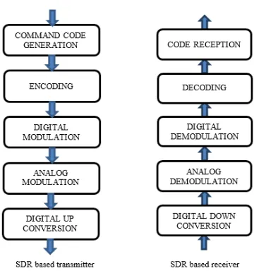
SDR Based Transmitter Algorithm:SDR based transmitter include command code generation, encoding, digital modulation, analog modulation and digital up conversion. The command codes are inputted from personal computer. For the demonstration purpose I used UART interface and send it through ARM LPC1769 to the FPGA board for further processing. The generated commands are a frame of N binary bits.The whole frame is encoded with Manchester encoding scheme and total number of bits in a frame becomes double, i.e., 2N. This Manchester encoded binary data waveform modulates a carrier signal using binary frequency shift keying (BFSK) modulation scheme. In this scheme, sinusoidal signal with higher frequency and lower frequency are generated for bit 1 and 0, respectively. This BFSK modulation is done in very low frequency, i.e., in very-low frequency band. This signal is finally up-converted to medium frequency band using frequency modulation (FM) scheme. The basic principle behind FM is to vary the carrier frequency in proportion to the modulating signal. FM modulated signal is the output of command code generator. This
signal undergoes digital up conversion (DUC).
To improve the sampling frequency of baseband signal interpolation is used. The primary reason to interpolate is to increase the sampling rate at the output of one system, so that another system operating at a higher sampling rate can operate the signal.
Fig. 1 SDR based transmitter and receiver
Fig. 1 shows the basic block diagram representation of SDR based transmitter and receiver.
III.IMPLEMENTATION OF SYSTEM
The system is implemented in FPGA. The entire system needs different frequencies such as 5 KHz as baseband data rate,1MHz as sampling frequency for BFSK modulation. 8 MHz as sampling frequency for FM modulation and 20 MHz for CIC interpolation module . The Spartan 3 FPGA board has global clock 30MHz. By using DCM in FPGA and clock generation module, required clocks are generated.
Digital Clock Manager (DCM): Spartan 3 has internal clock frequency of 30MHz. The 100MHz clock is generated from 30MHz clock using digital clock manager. In Xilinx clocking wizard general setup, input 30MHz as input clock frequency and input 100MHz as output clock frequency. All the remaining clocks are generated using clock generation sub module. Initially set count and clock as zero. Then increment the count. Select a value for the count in such a way that input clock period multiplied by that value should give required clock period. When the count equals selected value, take negation of clock and set count equal to zero. Then repeat the steps.
Transmitter and Receiver Side RTL Schematic: Register transfer level schematic of the transmitter and receiver side is shown in fig. 2.
Coding Principles Of Manchester Code: Manchester code is mainly used in digital systems. It is used to represent the binary values 0 and 1. It represent the binary values by a transition. The transition occurs at midbit, with low to high transition is used to represent a logic zero, and a high to low represent a logic one. A pattern of consecutive ones or zeros result in a transition on the cell boundary. When the data pattern alternates between one and zero, there is no transition at the cell boundary. Manchester code has no DC component, so it can be transformer coupled.The functions of the encoder section include a microprocessor interface, parallel to serial conversion, frame generation, and Manchester encoding. This circuitry does not require a high-frequency clock. The frame format used is similar to that of a UART.
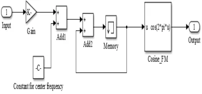
BFSK Modulation:Simulink model for the BFSK modulator is shown in Fig. 3The selected BFSK mark frequency is 50 KHz and space frequency is 10 KHz. By using a switch, if the Manchester encoded output is greater than 0, select constant for BFSK mark frequency and if it is zero, select constant for BFSK space frequency. It is given to the adder based on the output of Manchester encoder. Adder and memory together work as a phase accumulator. Cosine of the phase gives the modulated output.
Fig. 3 BFSK modulation
Block Memory Generator: Block memory generator is used to perform both BFSK and FM modulation. Xilinx provides a flexible Block Memory Generator core to create memories running up to 450 MHz. The Block Memory Generator IP core creates optimized block memories for Xilinx FPGAs. Block memory generator is selected from FPGA features and design. Component name is given as sine_table.
Memory Types: The Block Memory Generator core generates five types of memories: Single-port RAM, Simple Dual-port RAM, True Dual-Dual-port RAM, Single-Dual-port ROM, and Dual-Dual-port ROM. Here we need single Dual-port ROM.
Selectable Width and Depth: The Block Memory Generator core generates memories with 1 to 4608 bits width, and with depths of two or more words.Here we need to select read width in memory size as 10 bits and read depth in memory size as 32. The data that should be stored in ROM should store as .coe file in the ip core directive of FPGA. In the next step load the .coe file then click finish.
Frequency Modulation: Simulink model for the combined Manchester encoder and FM modulator is shown in Fig. 4. The selected FM deviation is 150 KHz. The output from BFSK modulator is multiplied with a gain K at a sampling rate of 8 MHz. A constant for FM deviation equal to 150 KHz is added with gain block output and is given to phase accumulator. Adder and memory together work as a phase accumulator. Cosine of the phase gives the modulated output.
Cascaded Integrator Comb Interpolator:A flexible, multiplier-free filter suitable for hardware implementation. It handle large rate changes. It is known as cascaded integrator comb filters, or CIC filters.The basic building blocks of a CIC filter are an integrator block and a comb block. When we build a CIC filter, we cascade N integrator sections together with N comb sections. We can “push” the comb sections through the rate changer, at the slower sampling rate
. Three things are accomplished here. First, half of the filter is slowed down and therefore efficiency is increased.Second, the number of delay elements required in the comb sections is reduced. Third, the integrator and comb structure are independent of the rate change. This means that we can design a CIC filter with a programmable rate change with the same filtering structure. The input of CIC interpolator is FM submodule output with 8 MHz sampling frequency. The output of CIC interpolator has 10 times the sampling rate as that of input wave. Output is seen on DSO and structure is shown in Fig. 5.
Fig. 5 CIC interpolator and decimator
CIC Decimator: The CIC Decimation block performs a sample rate decrease by an integer factor. The CIC Decimation block has the following CIC filter structure shown in Fig. 5. The structure consists of N sections of integrators, followed by a rate change by a factor R, and N sections of comb filters.The output of CIC decimator has 10 times reduced sampling rate as that of input wave.
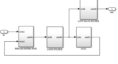
Frequency Demodulation: FM signal can be demodulated by applying the signal to the All-Digital Phase Locked Loop.
The All-Digital Phase Locked-Loop (ADPLL):The phase locked loop is useful in communication systems. It is used as a demodulator, where it follows phase or frequency modulation.The entire system is described in Verilog, the All-Digital Phase Locked Loop system is composed of four basic parts: Phase Detector (PD), Loop filter, Numerically-controlled oscillator (NCO) and Low Pass Output Filter. The complete block diagram of the Digital FM receiver circuit is shown in Fig. 6.
Fig. 6 The Digital FM receiver
Phase Detector:The Phase Detector (PD) detects phase error between output signal from NCO and the input. This operation employs a multiplier module and a register.
alpha=15/16=0.9375. This is a type of averaging with the smaller weights for the older values. It has a low pass filtering characteristics. After the multiplication done by the Phase detector, the loop filter will remove the high frequency components.
Numerically-Controlled Oscillator :Numerically-Controlled Oscillator (NCO) takes the corrective error voltage. Then it shifts its output frequency from its free- running value to the input signal frequency. The system is a integrator which accumulates the input value and maps it into a predefined cosine ROM. The look-up table with 1024 values which defines one cycle of cosine signal, is given in a separate file.
Low Pass Output Filter: The last stage of the FM demodulator system is low pass filter. It is used to perform signal shaping. 16 tap low pass filter is used to perform digital low pass filtering. This is an averaging filter. Its output is equal to the average value of its last n-input samples, where n is number of tap used. This filter needs 16 coefficients. For simplification, same value of the coefficients are assumed, i.e. 1/16. The 1/16 multiplication can be implemented by just 4bit right shift. Then no multiplier is required.
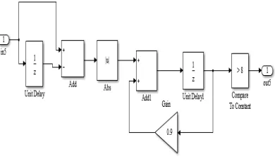
BFSK Demodulation: The BFSK demodulator composed of a high pass filter. It is used to filter out low frequency components of the digital signal. An absolute block to take absolute of the input signal. Further it includes a low pass filter. It is used to filter out high frequency components of the digital signal to produce a processed digital signal which indicates the baseband information in digital form. The block diagram for BFSK modulator is shown in Fig. 7.
Fig. 7 BFSK demodulator
Manchester Decoder: The decoder circuitry is more complex, since it require clock recovery and center sampling. The Manchester decoder uses a high-frequency clock. Additional functions of the decoder include frame detection, decoding of Manchester code, and serial to parallel conversion.The mdi1 and mdi2 registers have function similar to decoding circuitry which is used to detect an incoming edge on mdi (input of Manchester decoder, i.e. Manchester encoded data) and it activates the enable signal for the clk1x, i.e. clk1x_enable. When data is not being received, this enable signal reduces power consumption. The no_bits_rcvd keeps track of the number of bits received. To vary the word size to be received, change the value of no_bits_rcvd. The clkdiv register is used for the clock recovery.
Synchronization: To decode data correctly in the presence of noise is a design objective in serial communication. The signal value is indeterminate during non-zero rise and fall time. Decoding of the signal should occur as far from the signal transition in the receiver. Sampling at the time furthest from the signal transition is known as center sampling of the signal. A local clock which is 16X the received data rate is used for this purpose. The data format of a UART consists of a high idle state, start bit, five to eight data bits, optional parity, and one or more stop bits. First, an edge of a start bit is detected. Counting the 16X clock to 8 and verifying that the start bit is Low, so that the start bit is validated. Then the center samples are reached by counting the 16X clock to 16.In a Manchester decoder, center sampling occurs at 1/4 and 3/4 of the cell. Because transitions occur at mid-bit or on the cell boundary. In addition to center sampling, Manchester decoder does clock recovery. Manchester has transitions at least once each data cell. So the receiver can resynchronize at each bit.
The Manchester decoder uses a counter algorithm to synchronize to an incoming serial data stream. Counter algorithm which uses a 16x clock is given by two steps:
2. Reset the counter to 0. Count the 16x clock to 8 and sample. Reset the counter and go to (1) if there is a transition on Manchester data in.
IV.HARDWARE SETUP
The programming was done using Verilog on Xilinx ISE design suite version 14.5. The simulations are done in ISim simulator, it is included in the appendix. The project implemented on Spartan 3 xc3s200tqg144 board.
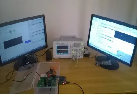
Experimental Setup: The system is implemented in a SPARTAN 3 FPGA board. The signal to be transmitted is given randomly and the output wave is observed using a Digital Spectrum Oscilloscope (DSO). The output is made analog using a R2R Digital to Analog Converter (DAC).The experimental setup is shown in the Fig. 8.
Fig. 8 Experimental Setup
Fig. 9 shows the device utilization summary of the implemented system in SPARTAN 3 FPGA board.
V. RESULT AND DISCUSSION
In the Fig. 10, it shows the Manchester encoded output for the input seven. It is displayed on DSO and verified the output.
Fig. 10 Manchester encoded output when input given is seven
Fig. 11 BFSK modulation output.
Verilog code for BFSK sub module is developed and implemented on FPGA. Output is seen from DSO. The DSO output is shown in Fig. 11.
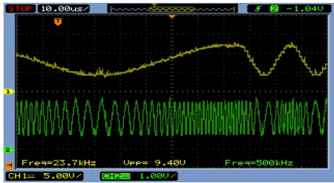
Fig. 12 Frequency modulator output on DSO
Fig. 13 Frequency demodulator output seen on simulator
The frequency demodulation circuit is modelled using Simulink. Output is shown in Fig. 13. Row one represent the transmitted signal. Row two represent the numerically controlled oscillator output which is similar to the input signal. Row three represent the output of phase detector, which is given to loop filter where averaging is taking place. The output of loop filter is given to low pass filter and BFSK modulated signal is getting as the output. Verilog code for FM demodulation is developed and implemented on FPGA.
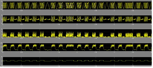
Fig. 14 BFSK demodulator output seen on simulator
In Fig. 14, it is shown that the BFSK demodulator output on simulator. Row one represent the input BFSK modulated signal. Row two represent the output of high pass filter where low frequency components are suppressed. Row three represent the output of absolute block, which is given to low pass filter where high frequency components are suppressed. Row four represent the output of low pass filter, which is given to threshold comparator. A suitable threshold is taken to decode the signal. Row five represent the Manchester encoded signal. Verilog code for FM demodulation is developed and implemented on FPGA.
VI.CONCLUSION
An SDR-based digital transceiver system is implemented. The system has been implemented using Xilinx FPGA, given a very highly flexible platform for complex algorithms for digital transceiver system designing. The system has been designed using Xilinx software. It provides a very reliable and fast communication. Suitable algorithms for signal generation, encoding, and baseband, and pass band modulation, DUC, DDC, demodulation and decoding of design have been chosen and implemented to ensure optimized uses of hardware.
REFERENCES
[2] T. Ulversoy, “Software defined radio: Challenges and opportunities,” IEEE Commun. Surv. Tuts., vol. 12, no. 4, pp. 531–550, 2010. [3] R. Woods, J. McAllister, Y. Yi, and G. Lightbody, “FPGA-Based Implementation of Signal Processing Systems”. Hoboken, NJ, USA: Wiley,
Oct. 2008, p. 65.
[4] J. Meier, R. Kelley, B. M. Isom, M. Yeary, and R. D. Palmer, “Leveraging software-defined radio techniques in multichannel digital weather radar receiver design,” IEEE Trans. Instrum. Meas., vol. 61, no. 6, pp. 1571 – 1582, Jun. 2012.
[5] V. B. Alluri, J. R. Heath, and M. Lhamon, “A new multichannel, coherent amplitude modulated, time-division multiplexed, software-defined radio receiver architecture, and field-programmable-gate-array technology implementation,” IEEE Trans. Signal Process., vol. 58, no. 10, pp. 5369–5384, Oct. 2010.
[6] Spartan-3 FPGA Family Data Sheet, DS099 June 27, 2013.
[7] Jin Li, YijunLuo, Mao Tian, “FM Stereo Receiver Based on Software-Defined Radio”, International Journal of Digital Content Technology and its Applications(JDCTA) Volume6,Number1,January 2012.
[8] Juan Pablo Martinez Brito, Sergio Bampi “Design of a Digital FM Demodulator based on a 2ndº Order All-Digital Phase-Locked Loop ”,PGMICRO – Graduate Program on Microelectronics.
[9] N. Jyothi, S. Jayaprakash, and S. K. Gowda, “Design and VLSI implementationofhighperformanceDUCandDDCforsoftware defined radio
applications,” in Proc. Int. Conf. Emerg. Trends Commun. Control Signal Process. Comput. Appl. (C2SPCA), 2013, pp. 1–3.
[10] M. Bernard-Schwarz, W. Zwick, L. Wenzel, J. Klier, and M. Groschl, “Field programmable gate array-assigned complex-valued computation and its limits,” Rev. Sci. Instrum., vol. 85, no. 9, pp. 093104–093104-6, 2014.
[11] C. R. A. Gonzalez, C. B. Dietrich, and J. H. Reed, “Understanding the software communications architecture,” IEEE Commun. Mag., vol. 47, no. 9, pp. 50–57, Sep. 2009.
[12] C. R. A. Gonzalez et al., “Open-source SCA-based core framework and rapid development tools enable software-defined radio education and