Design of Controlled Adder /Subtractor Cell
Using Shannon Based Full Adder
Sonika Choubey
1, Rajesh Kumar Paul
2PG Student [VLSI Design], Dept. of ECE, LNCT, Bhopal, India 1 Assistant Professor, Dept. of ECE, LNCT, Bhopal, India 2
ABSTRACT: This paper deals with design of controlled adder /subtractor cell using Shannon based full adder with pass transistor logic. The proposed adder used only 14 transistors for full adder implementation. Simulations were performed by Microwind 3.1 and DSCH 2 VLSI CAD tools and BSIM 4 for parametric analysis of various features. The analysis is done on the basis of power consumption, delay and area occupied and theses are compared with previous papers and we are good to enhance these parameters.
KEYWORDS:CAS, Shannon Theorem, Shannon Adder, BSIM4.
I. INTRODUCTION
In recent years, most of the VLSI applications, such as DSP and microprocessors use arithmetic operation like addition and subtraction.[1] .Many multiplier (or) divider circuits have been proposed that offer lower propagation delay, low power dissipation that can be implemented by using adder and subtractor. The high speed and reduced area size can be implemented with different logic style in VLSI design [3]. There are many types of logic designs, each has its own pros and cons in terms of speed, chip size (area) and power dissipation [4]. This trend must be ceased to obviate extortionate packaging and thermal management cost at system level. Eventually as more switching is done in a particular period of time; it would cause the circuit to perform much more gradual. However this quandary can be lowered if not solved by reducing the number of transistor that is being utilized. Many transistors in a circuit might be redundant and abstracting this redundancy can avail to lower the delay and hence incrementing the speed. This CAS cell is designed utilizing accumulation of full adder and 2 input XOR. The Shannon theorem predicated adder circuit can be reduced the number of transistor utilizing by redundancy reduction method.
The Shannon theorem adder circuit used only the NMOS, which would decrement the internal capacitance and reduce the propagation delay. The divider circuit parameters analysed utilizing by BSIM4 analyser. We have compared our results with three other adder cell predicated divider circuits in terms of speed, area and power dissipation.
II. FULL ADDER
A Full Adder is a basic cell component of the digital systems. It has three inputs and two outputs, sum and carry. It performs the addition of the three inputs and produces the sum and carry. The standard Boolean expressions are given as:
SUM = ABC+A’BC’+A’B’C+AB’C’ (1) CARRY = AB+BC+CA (2)
III. SHANNON BASED FULL ADDER
According to this theorem any logic expression is divided into two terms. First with a particular variable set to 1 and multiplying it by a variable and then set the variable to 0 and multiplying it by the inverse. The fullest reduction can be obtained by continuously repeating the Shannon theorem.
Copyright to IJAREEIE 10.15662/ijareeie.2015.0402033 739
f (b0, b1, b2, ..., bi,...y, bn) = bi’f (b0, b1, b2, ..., 0,...y, bn) + bi f (b0, b1, b2, ..., 1,...y, bn) (3) using Shannon expansion theorem we get modified full adder equation ,
SUM = 𝐴𝑥𝑜𝑟𝐵 𝐶 + (𝐴𝑥𝑜𝑟𝐵) C (4) and CARRY= 𝐴𝑥𝑜𝑟𝐵 𝐵 + 𝐴 𝑥𝑜𝑟 𝐵 𝐶 (5)
By using expressions (2) and (3), the pass transistor functions can be implemented as shown in Fig.1 ,this shows the Shannon based full adder design using pass transistor logic. [5]
Fig 1. Full adder implementation using pass transistor logic using 14-T
IV.PROPOSED ADDER/SUBTRACTOR CELL
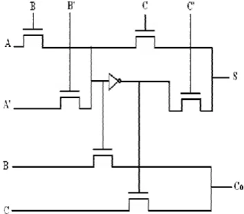
In digital circuits, an adder–subtractor is a circuit that is capable of integrating or subtracting numbers (in particular, binary). Below is a circuit fig 2 that does integrating or subtracting depending on a control signal. It is additionally possible to construct a circuit that performs both integration and subtraction concurrently.
Fig 2 Adder /Subtractor cell
that has control input D and the initial carry connect is also connected to D then:
When D=0 the modified adder performs addition
When D=1 the modified adder performs subtraction
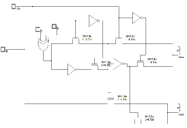
Fig 3. Schematic design of proposed CAS cell
In Fig 3 A and B, are one bit numbers used for addition / subtraction and cin is carry bit and T is test bit that is responsible for the behaviour of controlled adder/subtractor as a adder or subtractor .Sum/Difference and Carry/Borrow are output variables shown by LED outputs sum and carry . For verifying architectural behaviour simulation result is required so Fig 4 showing the simulation result done by using DSCH 2 tool for schematic design shown in Fig 3.
Fig 4 Simulation result of CAS cell using DSCH 2
V. RESULT AND DISCUSSION
Copyright to IJAREEIE 10.15662/ijareeie.2015.0402033 741
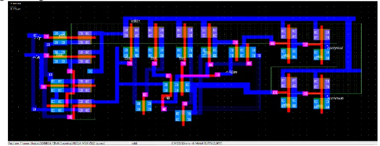
For designing and simulation of our circuit at physical description level here Microwind 3.1 software is going to use. Fig 5 showing the layout design of proposed CAS cell and fig 6 giving the simulation result for the layout .Fig 4 and 6 are verifying our design as a adder /subtractor cell .
Fig 5 Layout design of CAS cell on microwind 3.1
Here 65nm technology is used for implementing the design so corresponding supply voltage for above design is 0.7V and all parameter analysis is done by BSIM4 analyser that is inbuilt in Microwind 3.1 software.
Fig 6 Simulation Result of CAS cell on Microwind 3.1
VI.CONCLUSION
An adder circuit is designed by utilizing Shannon theorem and implemented into the design of adder/subtractor circuit. The proposed adder/subtractor circuit gives more preponderant performance. It compared its delay and area efficiency. Furthermore, this adder/subtractor cell can be use in divider, due to the utilization of Shannon predicated adder design approach . The proposed adder/subtractor circuit circuit may utilized in DSP circuits, divider and multipliers due to low power dissipation, less propagation delay and lower area.
REFERENCES
[1] Owk Prasanth Kumar ―Non-Restoring Divider Circuit Using a MCIT Based Adder Cell having Low Energy and High‖ International Journal of Scientific & Engineering Research Volume 3, Issue 4, April-2012 ISSN 2229-5518.
[2] C.Senthilpari, S.Kavithaa and Jude Joseph "lower delay and area efficient non-restoring array divider by usingshannon based adder technique" ICSE 2010 Proc. 2010, Melaka, Malaysia
[3] D. Markovic´ , B. Nikolic" V.G. Oklobdf ija, A general method in synthesis of pass-transistor circuits, Microelectr. J. 31 (2000) pp. 991—998. Kiat-seng Yeo and Kaushik roy "Low-voltage, low power VLSI sub systems"Mc Graw-Hill publication. ISBN: 0-07-143786-X
[4] R.Zimmermann,W.Fichtner,Low-power logic styles: CMOS versus pass-transistor logic, IEEE J. Solid-State Circuits 32 (7) (1997) pp. 1079— 1090.
[5] IACSIT International Journal of Engineering and Technology, Vol.2, No.3, June 2010 ISSN: 1793-8236A Shannon Based Low Power Adder Cell for Neural Network Training K.Nehru, Member, IACSIT, Dr.A.Shanmugam, S.Deepa and R.Priyadarshini.
[6] Qiao Tong and Niraj K. Jha "Design of C-Testable DCVS Binary Array Dividers" Volume 26, Issue 2, Feb. 1991 pp.134 — 141. [7] Scott C. Smith "Design of a NULL Convention Self-Timer Divider" ACM Conference proceeding ESA/VLSI 2004, pp. 447 — 453.
[8] Goel,S.Kumar,A.Bayoumi,M.A."Design of Robust, Energy- Efficient Full Adders for Deep-Submicrometer Design Using Hybrid-CMOS Logic Style" IEEE Transactions on Very Large Scale Integration (VLSI) Systems, Dec. 2006 Volume: 14, Issue: 12, pp. 1309-1321
[9] I-Chyn Wey; Chun-Hua Huang; Hwang-Cherng Chow "A new low- voltage CMOS 1-bit full adder for high performance applications" ASIC, 2002. Proceedings. 2002 IEEE Asia-Pacific Conference , 2002, pp. 21 — 24.
[10] M. Alioto, G. Palumbo, "Analysis and comparison on full adder block in submicron technology" IEEE Transactions on VLSI Systems, VOL. 10, NO. 6, DEC. 2002.
[11] Tung N. Pham Earl E. Swartzlander "Design of Radix 4 SRT
Dividers for Single Precision DSP in Deep Submicron CMOS Technology" Signal Processing and Information Technology, 2006 IEEE International Symposium on Publication Date: Aug. 2006 pp. 236-241.
[12] A.Th. Schwarzbacher, M. Brutscheck1, O.Schwinge,J.B.Foley "Constant Divider Structures of the Form 2n11 1" Irish Signals and Systems Conference 2000, Dublin, Ireland, pp. 368-375, June 2000.
[13] Donald A. Neamen "Microelectronics: Circuit-Analysis-andDesign"third international edition, ISBN 007-125443-9, 2007, pp. 137-139. [14] Wai-Kai Chen "the VLSI hand book 2nd edition" CRC press, Taylor & Francis Group 2007.
[15] Alioto, M.; Cataldo, G.D.; and Palumbo, G. (2007). Mixed full adder topologies for high-performance low-power arithmetic circuits.
Microelectronics Journal,38(1), 130-139
[16] Alito, M.; and Palumbo, G. (2002). Analysis and comparison of the full adder block. IEEE Transactions on VLSI, 10(6), 806-823.