BULLETIN NO. 230
642 MEMORY MAINTENANCE
64
2
MEMORY
ANAL YSIS OF MAINTENANCE TECHNIQUES
July
1958
MILITARY PRODUCTS DIVISION
INTERNATIONAL BUSINESS MACHINES CORPORATION
KINGSTON, NEW YORK
The work reported in this document was performed under a government contract. Information contained herein is of a proprietary nature. ALL INFORMATION CONTAINED HEREIN SHALL BE KEPT IN CONFIDENCE. No informa-tion shall be divulged to persons other than IBM employees authorized by the nature of their duties to receive such in-formation or individuals or organizations who are author-ized in writing· by the Department of Engineering or its ap-pOintee to receive such information. GOVERNMENT RE-LEASE MUST BE OBTAINED THROUGH THE CONTRACT ADMINISTRATION DEPARTMENT BEFORE THIS INFOR-MATION MAY BE USED FOR COMMERCIAL APPLICA-TIONS.
IBM
1r-1
KINGSTON~
UNCLASSIFIED
FOREWORD
This Instruction Bulletin represents the first of a series of four Instruction Bulletins, num-bered 230, 231, 232, and 233. They contain, in a convenient reference package, the pertinent maintenance information necessary to ensure the continued reliability of the 64 2 core memory element in the field.
Although each Instruction Bulletin is designed to be self -contained with regard to the subject matter covered, the FieldEngineer should famil-iarize himself initially with the contents of all four Instruction Bulletins in the series. This is recommended because in equipment as complex as memory there are many functions which are interrelated, and for which there are no clear-cut lines of demarcation. As a result, there are many items which are either cross-referenced directly or others, such as illustrations, which may be used as alternate references, if desired. In this manner, maximum benefit can be derived from the practical information presented.
The information contained herein supersedes the related text on maintenance techniques in the Preliminary Maintenance Data Book on Core Memory, and in T. O. 31P2-2FSQ7-142, dated April 1, 1957.
Heading
SECTION 1
1.1
SECTION 2
2.1
SECTION 3
3.1 3.2 3.2.1 3.2.2 3.2.3 3.2.4 3.2.5 3.2.5.1 3.2.5.2
SECTION 4
4.1
4.2
4.2.1
4.2.2
SECTION 5
5.1 5.2 5.3 5.4 5.5 5.6 5.6.1 5.6.2 5.6.3 5.6.4
5.7
UNCLASSIFIED
TABLE OF CONTENTS
INTRODUCTION .
Scope
PHYSICAL LAYOUT
Identification of Core Memory Element Components .
PROGRAMMING .
Maintenance Program Analysis .
Marginal Checking .
General.
Marginal Checking Facilities for Memory
Effect of Excursions on Memory Marginal Checking (MC) Lines.
Balance of Read and Write MGG Margins
Analysis of Printouts
Practical Cons iderations .
Typical Printouts
TROUBLESHOOTING TE CHNIQUES
Troubleshooting Solid Memory Failures .
Troubleshooting Intermittent Memory Parities .
Definition of Intermittent Memory Parities .
Recommended Action
ANALYSIS OF SUBTLE ELECTRICAL CHARACTERISTICS IN MEMORY .
Scope
MAR CPCF
Chatham Vs Tung-Sol 5998 Tubes .
Peaking Core Characteristics
PRF Conditions
Analysis of Various Timing Relationships
General.
Differences in Sample Time for Left and Right Half-Words.
Start- Memory Pulse.
Read and Write Current Widths .
DPD Decoupling .
Heading
5.7.1
5.7.2
5.8 Figure2-1
2-2
2-3 2-42-5
2-62-7
2-8 2-9 2-10 2-11 3-1 4-1 4-2 4-3 4-4 4-5 4-6 4-7 4-85-1
5-2
5-3 iiUNCLASSIFIED
TABLE OF CONTENTS (cont'd)
Fa ilure Symptoms Circuit Description .
Memory Array Floating Ground.
LIST OF ILLUSTRATIONS
Title
Core Memory Element, Pluggable Unit Side .
Core Memory Element, Wiring Stde
Memory Array Front View, Covers Removed
Memory Array Left Side View, Covers Remove'd
Memory Array Rear View, Covers Removed.
Memory Array Right Side View, Covers Removed e
Ferrite Core Memory Plane .
Address Selection
Memory Driver Panel, Address Locations
Layout of Memory Pluggable Units .
Z Module, Internal View
Typical Printouts Without and With Margins
Troubleshooting Flow Chart for Solid Memory Failures .
Troubleshooting Guide for Tim ing, Address ing, or Digit Failures
Memory Pulse Distribution, Waveform Analysis
Memory Driver Panel, Waveform Analysis .
Sense Amplifier, Waveform Analysis .
Signal Identification at the SA Output .
Typical Memory Waveforms .
Form for Logging Intermittent Memory Parities
Core Peaking Characteristics
Read and· Write Current Variations e
Current Unbalance with Program Content
UNCLASSIFIED
Page 42 42 45 Page 3 4 47/48, foldout49/50, foldout
51/52, foldout 53/54, foldout 5 6 7 8 9 21 23 55/56, foldout 26
27
28 2957/58, foldout
59/60, foldout
37
39
Figure
5-4
5-5
5-6
Table
2-1
2-2
2-3
2-4
2-5
2-6
3-1
3-2
3-3
4-1
4-2
UNCLASSIFIED
LIST OF ILLUSTRATIONS (cont'd)
Title
Relay Connections, DPD Decoupling
DPD Decoupling Circuitry, Simplified Diagram .
Memory Array Floating Ground .
LIST OF TABLES
Title
Circuit Identification, Unit 7 or 10, Module A
Circuit Identification, Unit 7 or 10, Module B
Circuit Identification, Unit 7 or 10, Module C
Circuit Identification, Unit 9 or 12, Module A
Circuit Identification, Unit 9 or 12, Module B
Circuit Identification, Unit 9 or 12, Module C
Memory Maintenance Programs
Memory Marginal Checking Lines
Analysis of Balancing Margins
Test Chart for Diode Matrix Decoder
.
Check List of Memory Trouble Areas .
UNCLASSIFIED
Page
43
44
46
Page
10
11
12
13
14
15
16
18
19
30
31
UNCLASSIFIED
UNCLASSIFIED
SECTION 1
INTRODUCTION
1.1 SCOPE
This Instruction Bulletin provides the information necessary for attaining a working knowledge of the 64 2 core memory element. It embodies the pertinent details pertaining to: physical configuration, maintenance programming, troubleshooting techniques, and analysis of subtle electrical characteristics. Specifically, these topics appear as follows:
Section 2 contains a pictorial layout of the physical components that constitute the 64 2 core memory element. Each component is then broken down into its constituent parts and identified.
Section 3 contains pertinent data relating to the identification and use of currently available maintenance programs. In addition, it incorporates an analysis of printouts and a discussion of marginal checking consistent with the concept of margin balanCing.
Section 4 contains a logical troubleshooting procedure supported by numerous photo-graphic references of waveforms obtained with a working memory.
Section 5 identifies the subtle type of electrical characteristics which may easily be over looked in analyzing memory malfunctions.
UNCLASSifiED
SECTION 2
PHYSICAL LAYOUT
2.1 IDENTIFICATION OF CORE MEMORY ELEMENT COMPONENTS
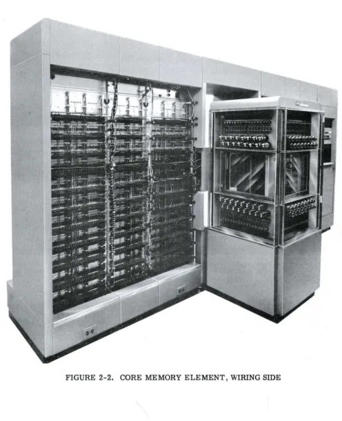
This section is intended to be self-explanatory since it features the physical layout of the c.ore memory element in pictorial form. A logical sequence. is employed commencing with the overan -front and back views of the core memory element in figures 2-1 and 2-2. A basic description of the other illustrations follows.
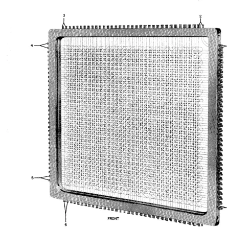
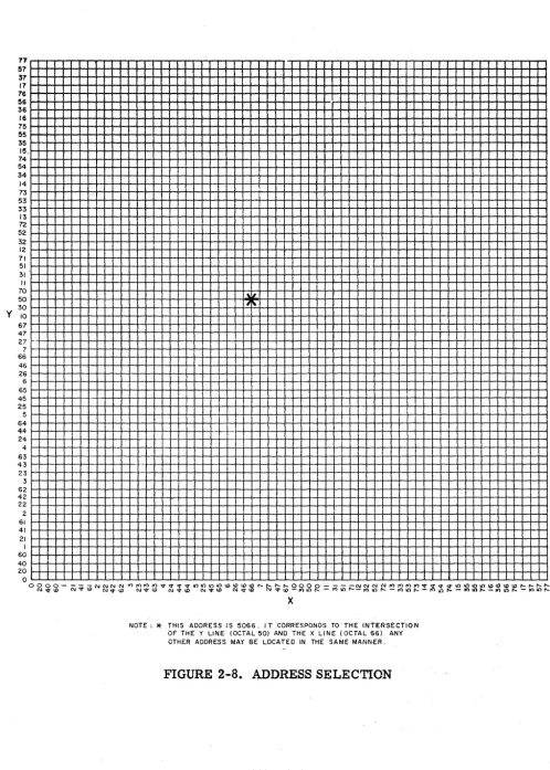
The memory array and its component details are shown separately_ in figures 2-3 through 2-6, foldouts. A further breakdown of the memory array is made in figures 2-7 and 2-8. The former figure illustrates the typical connections on a core memory plane (plane 5 is used as an example), while the latter figure depicts the physical lines in octal notation to facilitate finding the exact physical location for any given octal address.
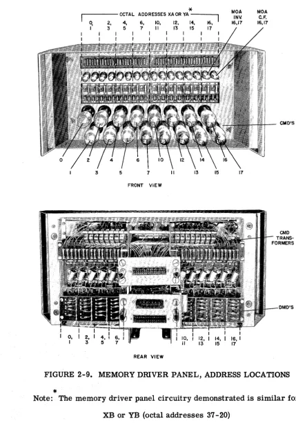
Figure 2-9 provides the front and rear views of the memory driver panel consistent with the identification of the components associated with the specific addresses provided by the memory driver panel. In this example, XA or YA memory driver panels are illustrated; however, the circuitry is similar for all memory driver panels with the
exception of the addresses assigned to each. These addresses are identified in figure 2-9.
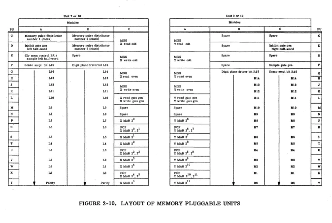
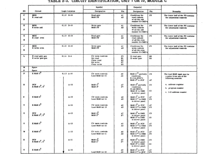
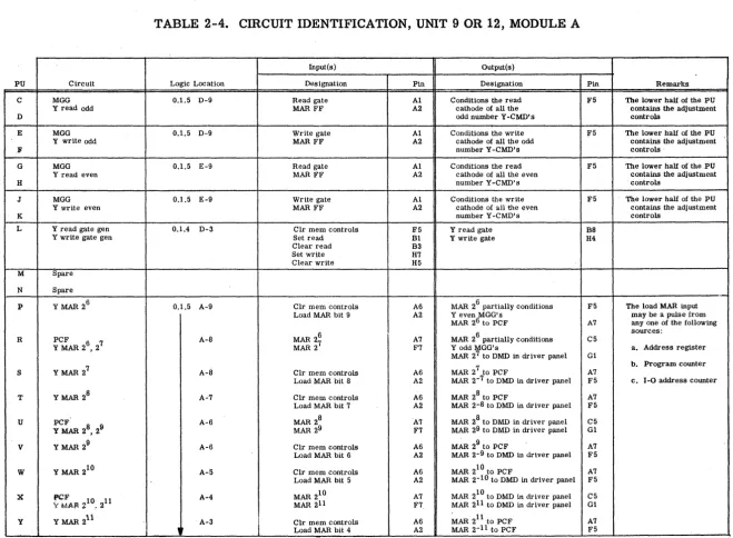
Figure 2-10 provides a detailed modular breakdown of units 7 or 10, 9 or 12, -and tables 2_-1 through 2-6 provide a further breakdown of the individual modules within these units. Fully identified are the circuit functions, location of applicable logic, the inputs and butputs for each individual pluggable unit, and any pertinent remarks that are helpful in better understanding the pluggable unit function.
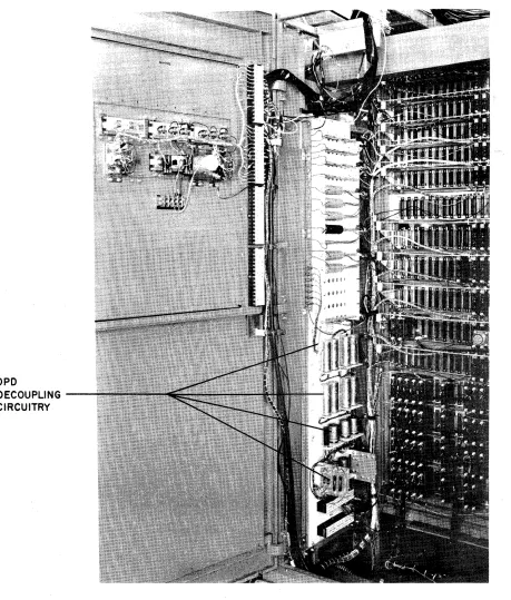
Figure 2-11 shows the components, particularly of the DPD decoupling circuitry, in the Z module.
UNCLASSIFIED
FIGURE 2-1. CORE MEMORY ELEMENT, PLUGGABLE UNIT SIDE
UNC
L
ASSIFIED
FIGURE 2-2. CORE MEMORY ELEMENT, WIRING SIDE
[image:10.611.40.536.102.712.2]UNCLASSIFIED
3 2
7
FIGURE 2-7. FERRITE CORE MEMORY PLANE
Note: The following legend is based on the analyzation of an odd plane (plane 5). A similar analysis is applicable between the corresponding-numbers of all other active planes.
1. Connection from DPD for the inhibit winding of plane 6.
2. Jumper from plane 5 to the inhibit winding of plane 6.
3. Inhibit winding connection for plane 5 jumpered from plane 6.
4. Sense winding connection for plane 5.
5,6,7. Jumpers within plane 5.
[image:11.632.71.515.44.536.2]Y
UNCLASSIFIED
77 57 37 17 76 56 36 16 75 55 35 15 74 54 34 14 73 53 33 13 72 52 32 12 71 51 31 II 70 50 30 -',~ 7\-10 67 47 27-7 66 46 26 6 65 45 25 5 64 44 24 4 63 43 23 3 62 42 22 2 61 41 21 I 60 40 20 o °2~g-N~~N~*~~~~~~~~~~~~~~~*~~~~~2~2~=~~~~~~~~~~~~~~~~~~~~~~~~~~~
x
NOTE;
*'
THIS ADDRESS IS 5066. I T CORRESPONDS TO THE INTERSECTION OF THE Y LINE (OCTAL 501 AND THE X LINE (OCTAL 661. ANY OTHER ADDRESS MAY BE LOCATED IN THE SAME MANNER.FIGURE 2-8. ADDRESS SELECTION
[image:12.627.45.543.68.765.2]UNCLASSIFIED
*
. - - - OCTAL ADDRESSES XA OR VA - - - . , MOA INV. 16,17
3 5 7 II 13 15 17
FRONT VIEW
0, 2,
I 3
I 1 I
12, I 14, I 16,1 13 15 17
REAR VIEW
MOA
C.F. 16,17
CMD
TRANS-FORMERS
DMD'S
FIGURE 2-9. MEMORY DRIVER PANEL, ADDRESS LOCATIONS
*
Note: The memory driver panel circuitry demonstrated is similar for
XB or YB (octal addresses 37 -20)
XC or YC (octal addresses 57 -40)
XD or YD (octal addresses 60-77)
[image:13.615.78.507.61.673.2]co
Unit 7 or 10 Modules
PU A B
C Memory pulse distributor Memory pulse distributor number 1 (clock) number 2 (clock) D Inhibit gate gen Memory pulse distributor
left half-word number 3 (clock)
E Clr mem control PA's Spare sample left half-word
F Sense ampl bit LI5 Digit plane driver bit LI5
G LI4 LI4
r
-H LI3 LI3
-J LI2 L12
-K Lll Lll
-L LI0 LID
-M L9 L9
-N La La
----
P L7 L7~
R L6 L6
!
-S L5 L5
r
-T L4 L4
'
-U L3 L3
r
-V L2 L2
~
W Ll Ll
r----X I.8 I.8
i---Y Parity
,
ParityFIGURE 2-10.
Unit 9 or 12 Modules
C A B
Spare
MOO MOO
X read odd Yread odd
Spare
MGG MOO Spare
X write odd Y write odd
Spare
MOO MGG Digit plane driver bit R15
X read even Y read even
Rl4
MOO MOO R13
X write even - Ywrite even
Rl2
X read gate gen Y read gate gen Rll
X write gate gen Y write gate gen
Spare Spare RI0
Spare Spare R9
X MAR 20 Y MAR 26 R8
PCF
X MAR 20, 21 PCF Y MAR 26, 27 R7
X MAR 21 Y MAR 27 R6
X MAR 22 Y MAR 28 R5
PCF
X MAR 22, 23 iC~ 28 29 R4
X MAR 23 Y MAR 29 R3
X MAR 24 Y MAR 210 R2
PCF X MAR 24,25
PCF
Y MAR 210, 211 Rl
X MAR 25 Y MAR 211
• as
LAYOUT OF MEMORY PLUGGABLE UNITS
C Spare
Inhibit gate gen right half-word Spare
Sample gate gen Sense ampl bit Rl5
Rl4 Rl3 Rl2 Rll RIO R9 R8 R7 R6 R5 R4 R3 R2 RI
• as
PU C D E F G ~
-
J -K-
L -III-
N ~ P ~ RI
-S
I
-T
i -U i -V
-
W -X -yc
Zn
....
»
( I '
'"
-:!! m
[image:14.793.68.742.78.532.2]UNCLASSIFIED
DPD
DECQUPLING -CIRCUITRY
FIGURE 2-11. Z MODULE, INTERNAL VIEW
[image:15.612.70.529.117.656.2]...
o PU C D E F G H J K L M N P R S T U V W X yTABLE 2-1. CIRCUIT IDENTIFICATION, UNIT 7 OR 10, MODULE A
Input(s) Output(s)
Circuit Logic Location Designation Pin Desirnation Pin Remarks
Memory pulse distributor 0.1.4 A-4 Start memory B2 Set react A2
number 1 (clock) Sample Jl
Clear read E5
To memory pulse distributor 2 Gl
Inhibit gate gen 0.1.4 D-2 Set inhibit At Inhibit gate H6
left half-word Clear inhibit A5
Clr mem controls Bl
Clr mem controls PA's 0.1.4 C-5 Clr mem controls A5 Clear inhibit & sample gate gen A6
Sample left half-word RD D-l Sample left half-word H6 Clear Y MAR, read & write
gate gen B8
Clear X MAR, read & write
gate gen F5
Sample left half-word H3
Sense ampl bit L15 0.1.6 A-8 to E-8
Output of Plane 3 Al,A2 Sense ampl test-point G2
A5,A6 Output to memory buffer H8
Sample pulse H5
J,J4 Plane 5
L13 Plane 7
L12 Plane 9
Lll Plane 11
LlO Plane 13
L9 Plane 15
L8 Plane 17
L7 Plane 19
L6 Plane 21
L5 Plane 23
L4 Plane 25
L3 Plane 27
L2 Plane 29
Ll Plane 31
LS Plane 33
TABLE 2-2. CIRCUIT IDENTIFICATION, UNIT 7 OR 10, MODULE B
input(s) Output(s)
PU Circuit Logic Location Des ignation Pin Des ignation Pin Remarks
C Memory pulse distributor 0.1.4 A-3 From memory pulse distrib- Fl SeL innibit E5
number 2 (clock) utor number 1 Sct write Cl
To memory pulse distributor 3 A3
D Memory pulse distributor 0.1.4 A-2 From memory -pulse diStrib- A5 Clear inhibit E8
number 3 (clock) utor number 2 Clear write B4
E Spare
F Digit plane driver bit LI5 0.1.6 A-4 to E-4 Level from memory buffer A6 Signal to inhibit winding F6
Inhibit gate A7 of Plane 3
via Plane 4
G L14 of Plane 5 The inhibit signal path for the
via Plane 6 left half-word is as follows:
H L13 of Plane 7 From Pin F6 of the DPD
via Plane 8 pluggable unit to an even-numbered plane on the array,
J L12 of Plane 9 then to the desired
odd-via Plane 10 numbered plane immediately above it and through all the
c
c
z
ZK L11 of Plane 11 cores in the desired plane,
n
via Plane 12 back down to the even-n
r-
r-numbered plane from which
L LlO of Plane 13 point it is routed to the
via Plane 14 inhibit current terminating resistor.
>
>
(.n (.n
(.n (.n
M L9 of Plane 15
via Plane 16
~ ~
m m
N L8 of Plane 17
o
0via Plane 18
p L7 of Plane 19
via Plane 20
R L6 of Plane 21
via Plane 22
S L5 of Plane 23
via Plane 24
T L4 of Plane 25
via Plane 26
U L3 of Plane 27
via Plane 28
V L2 of Plane 29
via Plarie 30
W Ll of Plane 31
via Plane 32
.x LS of Plane 33
via Plane 34
y.
,
Parity of Plane 35c
Zn
...
l> ~ ~-
:!! m C PU C 0 E F G H J K L M N P R S T U V W X y Circuit MOOX read odd
MOO
X write odd
MOO
X read even
MOO
X 'write even
X read gate gen X write gate gen
Spare Spare X MAR 2U.
PCF X MAR 2°, 21
X MAR 21
X MAR 22
PCF X MAR 22, 23
X MAR 23
X MAR 24
PCF 4 5 XMAR2,2
X MAR 25
TABLE 2-3. CIRCUIT IDENTIFICATION, UNIT 7 OR 10, MODULE C
Input(s) Output(s),
Logic Location Designation Pin Designation Pin Remarks
0.1.5 0-16 Read gate Al Conditions the F5 The lower half of the PU contains MARFF A2 read cathode the adjustment controls
of all the odd number X-CMO's
0.1.5 0-16 Write gate Al Conditions the F5 The lower half of the PU contains MARFF A2 write cathode the adjustment cootrols
of all the odd number X-CMD's
0.1.5 E-16 Read gate Al Conditions the F5 The lower half of the PU contains MARFF A2 read cathode the adjustment cootrols
of all the even number X-CMD's
0.1.5 E-16 Write gate At Conditions the F5 The lower half of the PU contains MARFF A2 write cathode the adjustment controls
of all the even number X-CMD.'s 0.1.4 0-4 Clr mem controls F5 X read gate B8
Set read Bl X write gate H4 i
Clear read B3
Set write H7
Clear write H5
0.1.5 A-16 Clr mem controls A6 MAR 2 -0 partially F5 The load MAR input may be Load MAR bit 15 A2 conditions a pulse from any of the
X even MGG's following sourc.es: MAR 20 to PCF A7
A-I5 MAR 20 A7 MAR 20 partially C5 a. address register MAR 21 F7 conditions b, program counter
X-odd MGG's MAR 21 to DMD G1
1-0 address counter in driver panel c.
A-15 Clr mem controls A6 MAR 21 to PCF A7 Load MAR bit 14 A2 MAR 2- 1 to DMD F5
in driver panel A-14 Clr mem controls A6 MAR 22 to PCF A7
Load MAR bit 13 A2 MAR 2- 2 to DMD F5 in driver panel
A-13 MAR 22 A7 MAR 22 to DMD C5
MAR 23 F7 in driver panel MAR 23 to DMD G1
in driver panel A-13 Clr m.em controls A6 MAR 23 to PCF A7
Load MAR bit 12 A2 MAR 2-3 to DMD F5 in driver panel
A-12 ell' merl' controls A6 MAR 24 to PCF A7
Load MAR bit 11 A2 MAR 2-4 to DMD F5
in driver panel
A-ll MAR 24 A7 MAR 24 to DMD C5
MAR 25 F7 in driver panel MAR 25 to DMD Gl
in driver panel
A-tO A6 MAR 25 to PCF A7
1 Load MAR bit 10 A2 MAR 2- 5 to fCF F5
[image:18.799.51.750.47.544.2]TABLE 2-4. CmCUIT IDENTIFICATION, UNIT 9 OR 12, MODULE A
Input(s) output(s)
PU Circuit Logic Location Designation Pin Designation Pin Remarks
C MOO 0.1.5 D-9 Read gate Al Conditions the read F5 The lower half of the PU
Y read odd MARFF A2 cathode of all the contains the adjustment
D odd number Y -CMD' s controls
E MOO 0.1.5 D-9 Write gate Al Conditions the write F5 The lower half of the PU
Y write odd MARFF A2 cathode of all the odd contains the adjustment
.If number Y-CMD's controls .
G MGG 0.1.5 E-9 Read gate A1 Conditions the read F5 The lower half of the PU
Y read even MAR FF A2 cathode of all the even contains the adjustment
H number Y -CMD' s controls
J MGG 0.1.5 E-9 Write gate Al Conditions the write F5 The lower half of the PU
Y write even MARFF A2 cathode of all the even contains the adjustment
K number Y -CMD's controls
L Y read gate gen 0.1.4 D-3 Clr mem controls F5 Y read gate BS
Y write gate gen Set read B1 Y write gate H4
Clear read B3
Set write H7
Clear write H5
M Spare
N Spare
P Y MAR 26 0.1.5 A-9 Clr mem controls A6 MAR 26 partially conditions F5 The load MAR input
Load MAR bit 9 A2 Y even MGG's may be a pulse from
MAR 26 to PCF A7 anyone of the following
MAR 26 MAR 26 partially conditions
sources:
R PCF A-a A7 C5
Y MAR 26,27 MAR 27 F7 Y odd MGG's a. Address register
MAR 27 to DMD in driver panel Gl
Y MAR 27 MAR 27 to PCF
b. Program counter
S A-a Clr mem controls A6 A7
Load MAR bit 8 A2 MAR 2-7 to DMD in driver panel F5 c. 1-0 address counter
T Y MAR 28 A-7 Clr mem controls A6 MAR 28 to PCF A7
Load MAR bit 7 A2 MAR 2- 8 to DMD in driver panel F5
U PCF A-6 MAR 28 'A7 MAR 28 to DMD in driver panel C5
Y MAR 28, 29 MAR 29 F7 MAR 29 to DMD in driver panel Gl
V Y MAR 29 A-6 Clr mem controls A6 MAR 29 to PCF A7
Load MAR bit 6 A2 MAR 2- 9 to DMD in driver panel F5
W Y MAR 210 A-5 Clr mem controls A6 MAR 210 to PCF A7
Load MAR bit 5 A2 MAR 2- 10 to DMD in driver panel F5
X fCF A-4 MAR 210 A7 MAR 210 to DMD in driver panel C5
y. MA.~ 210. 211 MAR 211 F7 MAR 211 to DMD in driver panel Gl
Y Y MAR 211
,
A-3 Clr mem controls A6 ~AR 211 to PCF A7 [image:19.797.63.723.71.555.2]PU Circuit
C Spare
D Spare
E Spare
F Spare
G Digit plane driver bit Rl5
H Rl4
J Rl3
K Rl2
L Rll
M RIO
N R9
P R8
R R7
S R6
T R5
U R4
V R3
W R2
X R1
y RS
•
TABLE 2-5. CIRCUIT IDENTIFICATION, UNIT 9 OR 12, MODULE B
Input(s) Output(s)
Logic Location Designation Pin Designation Pin
0.1.6 A-2 to E-2 Level from memory buffer A6 Signal to inhibit winding
Inhibit gate A7 of Plane 4 F6
via Plane 3
of Plane 6 via Plane 5
of Plane 8 via Plane 7
of Plane 10 via Plane 9
of Plane 12 via Plane 11
of Plane 14 via Plane 13
of Plane 16 via Plane 15
of Plane 20 via Plane 19
of Plane 22 via Plane 21
of Plane 24 via Plane 23
of Plane 26 via Plane 25
of Plane 28 via Plane 27
of Plane 30 via Plane 29
of Plane 32 via Plane 31'"
of Plane 34 via Plane 33
of Plane 36
"
l'
",
via Plane 35"
Remarks
The inhibit signal path for the right half-word is as follows: From pin F6 of the DPD
TABLE 2-6. CIRCUIT IDENTIFICATION, UNIT 9 OR 12, MODULE C
lnput(s) Output(s)
PU Circuit Logic Location Desi!mation Pin Desi:],nation Pin Remarks
C Spare
D Inhibit gate gen 0.1.4 D-2 Set inhibit A1 Inhibit gate H6
right half-word Clear inhibit A5
Clr mem controls B1
E Spare
F Sample gate gen 0.1.4 D-2 Clr mem controls B1 Sample right half-word F7
Inhibit sample C7 Sample left half-word F5
Clear write A5
Sample pulse A8
G Sense ampl bit R15 0.1.6 A-6 to E-6 Output of Plane 4 Al,A2 Sense ampl test-point G2
A5,A6 Output to memory buffer H8
Sample pulse H5
c
c
z
Zn
n
H R14 Plane 6
r-
r-J R13
>
Plane 8>
c.n c.n
c.n c.n
K R12 Plane 10
-~ ~
L Rll Plane 12
m m
C C
M RlO Plane 14
N R9 Plane 16
P R8 Plane 20
R R7 Plane 22
S R6 Plane 24
'I' R5 Plane 26
U R4 Plane 28
V R3 Plane 30
W R2 Plane 32
X R1 Plane 34
y ~ RS
,
~ Plane 36UNCLASSIFIED
SECTION 3
PROGRAMMlNG
3.1 ,MAINTENANCE PROGRAM ANALYSIS
There are varied maintenance programs available for testing the core me.mory element. Each has been written to provide a specific analysis of equipment performance. As a result, they run the gamut in size and scope from small and simple, to large and complex, depending upon their objective.
To obtain maximum benefit from these memory programs requires an awareness not only of their existence but, more important, of their intended functions and assumptions. Although detailed information regarding any memory program is provided in the program writeup, a brief functional description of the memory programs currently in us e is pro-vided in table 3-1. Program identification in this table is limited to the basic program type without reference to the latest level.
Program Type
MC 1 MEM 01
MC MEM PAR 01
16
TABLE 3-1. MEMORY MAINTENANCE PROGRAMS
Function
This is the major memory program. It is designed to test the over-all reliability of the core memory element including over-all the lines within the MC group 1. It is loaded into one core memory and con-ducts checks on the second core ·memory. Each core is tested with worst patterns. The program' contains 11 routines designed to test the memory under the most stringent conditions. For example, in the PRF routine, the 10 register is used to read all O's into memory at a 6 usec rate; failure here may indicate that the areas under the read and write currents are not equal, or that the timing is incorrect at the end of the memory cycle due to improper setting of the clear-inhibit and clear -write puls es .
This program is designed to supplement MC-l MEM 01. It tests only the parity plane, and its associated sense amplifier and digit plane driver. It contains a PRF and four worst pattern tests on the parity bit. Marginal checks are performed only using the -150 Cl (SA) and -300 Al (DPD) lines. It has all the SENSE switch options of MC-l MEM 01 except X printout suppression.
UNCLASSIFIED
TABLE 3-1. MEMORY MAINTENANCE PROGRAMS (cont'd)
Program Type
MEMORY 04
MEMORY 05
MEMORY 06
Function
This is a general reliability type program which is loaded into and tests the same memory. As a result, no automatic margins are
applied because the program is in the memory under test. Since ~ only one memory is used, it is very useful during installation. From experience, this program has detected some errors missed by Me-1 MEM 01. The possible reasons advanced for this phenomenon
follow:
a. MEM 04 uses three start-memory pulses: from the program counter, address register, and 10 address counter. MEM 01, however, uses only the latter two to start the memory under test.
b. MEM 04 in spot checking for worst patterns and relocating itself may set up unique PRF conditions.
c. MEM 04 reads in information from the card reader on a stag-gered basis (exercises memory in a manner similar to program
MEM 06).
This program is designed to detect failures due to faulty peaking cores; that is, if all other programs work and this one fails, it is an indication to check the cores. It loads into one memory and checks the other. It is the only memory program that uses drums. It applies margins only to the -150 C1 (SA CF) -300 B1 (write MGG's) and -300 B2 (read MGG's) Me lines. It sets up PRF conditions USing patterns consisting of read O-write 1 and read 1-write
a
at a rate that is' less than 10 usec due to the use of drums.This program was designed primarily to detect low frequency oscillation in the sense amplifiers. It does this by operating the sense amplifiers at a 6 usec rate, then by idling them for varying periods of time, and then by operating them again at a 6 usec rate. The time delay is varied by maintenance console switches. Two memories are necessary. No margins are applied.
3.2 MARGINAL CHECKING
3.2.1 General
The marginal checking facilities built into the computer are used to provide a high degree of reliability in the core memory element circuits. Marginal checking is per-formed by varying a supply voltage to a group of circuits. The variation of the supply voltage is called an excursion. The magnitude of an excursion necessary to produce operational circuit failure is called a margin.
3.2.2 Marginal Checking Facilities for Memory
The marginal checking lines for the core memory element are summarized in table 3-2. As shown, the circuit groups are divided equally between memory 1 and memory 2. This circuit group breakdown serves only to differentiate between the two memories for ideritification purposes; for example, -300B1 (memory 1) corresponds directly to -300E1 (memory 2); 150A1 (memory 1) corresponds directly to 150D1 (memory 2); 90el (memory 1) corresponds directly to 90Fl (memory 2); etc.
UNCLASSIFIED
TABLE 3-2. MEMORY MARGINAL CHECKING LINES
Unit MC Group Circuit Group Lines
MEMORY 1 1 A 1 through 6
B 1 through 6
C 1 through 6
MEMORY 2 1 D 1 through 6
E 1 through 6
F 1 through 6
3.2.3 Effect of Excursions on Memory Marginal Checking (MC) Lines
The memory
1\'19
lines may be functionally divided into two basic categories: diagnostic lines and system lines. A description of each follows:a. A diagnostic line is one whose printout usually indicates that the circuit to which an excursion is applied is defective and the
associated pluggable unit is to be replaced as the initial corrective step. All of the MC lines fall into this category with the exception of three system lines to be discussed later. One of the most
important diagnostic lines is the DPD -300A1 (D1) line. For this line, a negative excursion (which is the only one applied) causes the . inhibit current to decrease in amplitude slightly; however, its
principal effect is reduction of the inhibit current pulse width.
As a result, when failure occurs, it is usually due to improper overlap of inhibit current on write current.
b. The system lines encompass three MC lines; -150 C1 (F1), -300Bl (E1), and -300 B2 (E2). The effect of excursions on these lines will be discussed separately:
1. An excursion on the -150 Cl (F1) line tends to vary the sense amplifier voltage level of the waveshape appearing at pin G2. Hence, a positive excursion picks up noise or 0 as a 1. A negative excursion has the effect of dropping a 1.
2. An excursion on the -300 Bl (El) line varies the MGG write currents as follows: A positive excursion has the effect of decreasing the write current approximately 1 ma/volt. A negative excursion has the effect of increasing the write current apprOXimately 1 ma/volt.
3. An excursion on the -300 B2 (E2) line varies the MGG read currents in the same direction and by the same amounts as noted above for the write currents.
3.2.4 Balance of Read and Write MGG Margins
During normal operation (DCS, DCA, or any program), the read or write currents may increase above their nominal values due to PRF c,onditions (refer to 5.5 for detailed explanation). This means that the read and write currents due to program content vary
UNCLASSIFIED
in a manner similar to that experienced while applying excursions to the -300 B1 (El) and -300 B2 (E2) MC lines. This fact serves to emphasize the importance of maintaining read and write margins that are larger than the excursions produced by the program.
If time is ava:ilable, it is not sufficient to maintain the -300 B1 (E1) and -300 B2 (E2) MC lines at prescribed margins. Instead, the margins should be made as high as possible by generally striving for the following goals:
1. Try to obtain a large spread; that is, -35V + 45V is equal to a spread of BOV.
2. Consistent with the large spread, try for balanced margins; that is, -40V + 40V represents a perfect balance with the spread remaining at BOV.
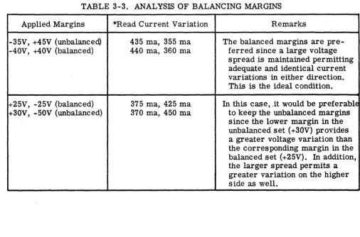
To fully understand the underlying principles involved, some practical applications are considered in table 3-3. This table lists four sets of margins that provide widely separated examples of conditions that may be encountered. For each particular set of margins an analysis is made in the remarks column regarding which of the margins is
considered more preferable and the reason for its selection.
The conclusions to be drawn from table 3-3 are that when balancing margins, the choice should be predicated on obtaining the highest margins in both directions. For un-balanced margins, it must be recognized that it is always the lower of the two margins that is the critical factor in determining equipment susceptibility to failure.
TABLE 3-3. ANALYSIS OF BALANCING MARGINS
Applied Margins *Read Current Variation Remarks
-35V,+45V (unbalanced) 435 ma, 355 ma The balanced margins are pre--40V, +40V (balanced) 440 rna, 360 rna ferred since a large voltage
spread is maintained permitting adequate and identical current variations in either direction. This is the ideal condition.
+25V, -25V (balanced) 375 ma, 425 rna In this case,.it would be preferable +30V, -50V (unbalanced) 370 rna, 450 ma to keep, the unbalanced margins
since the lower margin in the unbalanced set (+30V) provides a greater voltage variation than the corresponding margin in the balanced set (+25V). In addition, the larger spread permits a greater variation on the higher s ide as well.
[image:25.618.65.572.405.739.2]UNCLASSIFIED
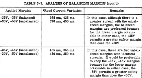
TABLE 3-3. ANALySIS OF BALANCING MARGINS (cont'd)
Applied Margins *Read Current Variation Remarks
+35V, -35V (balanced) 365 ma, 435 ma In this case, although tliere is a +30V, -50V (unbalanced) 370 ma, 450 Ilia greater spread with the
unbal-anced margins, the balunbal-anced margins are preferred because for the lower margin obtain-able in either case, the +35V permits a greater safety margin than does the +30V.
-35V, +45V (unbalanced) 435 ma, 355 ma In this case, there are.two unbal--30V, +50V (unbalanced) 430 ma, 350 ma anced margins with identical
spreads. It would be preferable to keep the -35V, +45V margins because for the lower margin obtainable in either case, the -35V permits a greater safety margin than does the -30V.
*Based on an initial adjustment of read current equal to 400 ma, and the assumption that a negative excursion of
tv
is equal to alma increase in current, and that a positive excursion of 1 V is equal to alma 'decrease in current.3.2.5 Analysis of Printouts
3.2.5.1 Practical ConSiderations
From experience, it has often proven advantageous to take the following action when confronted with printouts while running Me -1 MEM 01:
1 e If it begins to printout, it is advisable to continue the program through
to its completion. In this manner, a complete picture of the situation is made available before instituting corrective measures.
2. If,in a certain routine, a printout to prescribed is difficult to analyze, it is recommended that a higher margin be applied manUally. This proc~dure may then provide a printout in a different routine that is easier to diagnose.
3. If an addressing failure results in a printout, it may be difficult to analyze. Under these conditions, memory driver panel replacement or substitution is recommended.
3.2.5.2 Typical Printouts
Typical printouts with and without margins are exemplified in figure 3-1. They are representative of the printouts obtained when the printer panel is wired for an octal split.
[image:26.618.50.542.66.337.2]c:
Zn
r-»
""
""
-::r! m CPRINTOUT 17777 O. 000 000 000 000 000 O. 100 000 000 000 000
EXPLANATION Y X ADDRESS OF
FAILING LOCATION
CONDITION LIGHTS THAT GO ON AT TIME
THESE ARE THE CONTENTS OF THE FAILING LOCATIONS.
PRINTOUT
LEGEND: (ABOVE) (BELOW)
OF FAILURE. THEY SHOW ROUTINE BEING RUN
PRINTOUT WITH NO APPLIED MARGINS
FROM THIS» THE BITS IN ERROR CAN BE DETERMINED
IN ADDITION TO THE ABOVE TYPE OF INFORMATION, THE FOLLOWING PRINTOUT IS ALSO PROVIDED IF MARGINS ARE APPLIED AT THE TIME OF FAILURE
02566 , B un +090
EXPLANATION THIS IS THE STEP BRANCH ED FROM AT TIME OF FAILURE;
GROUP CIRCUIT LINE VOLTAGE
IT ALSO SHOWS ROUTINE BEING RUN SINCE IT IS FOUR LESS THAN NORMAL ERROR HALT FOR THAT ROUTINE. IN
THIS EXAMPLE, 02572 IS THE ERROR HALT FOR THE REGULAR CHECKERBOARD ROUTINE
(APPLIED MARGINS AT TIME OF FAILURE)
FIGURE 3-1. TYPICAL PRINTOUTS WITHOUT AND WITH MARGINS
-018
[image:27.812.49.733.66.544.2]UNCLASSIFIED
SECTION 4
TROUBLESHOOTING TECHNIQUES
4.1 TROUBLESHOOING SOLID MEMORY FAILURES
Logical troubleshooting requires that all information capable of detecting an error . be analyzed on a systematic, step-by-step basis. The information presented in the
sub-sequent steps is predicated on this concept, and must be performed in the order given to achieve maximum benefit in isolating solid memory failures. A summary of the pertinent troubleshooting procedures is shown in figure 4-1. Each block in the figure is numbered to correspond to the detailed procedural steps that follow:
22
1. Determine if a t.rue memory parity exists. This can be ascertained by diagnosing the symptoms that differentiate between a false and true memory parity, as follows:
a. It is a false memory parity if, at the time of computer halt on memory parity, the word in the memory buffer register is a good parity word. For this condition the trouble is not usually in memory but in the Central Computer parity count and asSign circuitry.
b. It is a true memory parity if, at the time of computer halt on memory parity, the word in the memory buffer register is:
(1) All O's, including the parity bit. This indicates trouble may be in either the memory buffer register, memory, or a miSSing start-memory pulse.
(2) A bad parity word other than all 0' s . This indic ates trouble may be in either the memory buffer register, memory, or a missing inhibit-sample pulse.
If a true memory parity eXists, proceed with the next step:
2 Determine whether the failure is isolated to one memory or both memories. If the failure is common to both memories, it usually is not a memory trouble but rather a Central Computer trouble in any of the following areas: memory buffer register, a miss ing start-memory pulse, or a miSSing inhibit-sample pulse.
If the failure occurs in only one memory, proceed with the next step:
3. Determine whether program MC-1 MEM 01 will fail without margins. For this check, it is recommended that the program
NOTE:
• REFER TO TEXT FOR DETAILED DESCRIPTION OF EACH NUMBERED BLOCK
UNCLASSIFIED
MEMORY PARITY
NO
NO
YES
YES
NO
NO
NO
NO
NO
NO
YES
NO
FIGURE 4-1. TROUBLESHOOTING FLOW CHART FOR SOLID :MEMORY FAILURES
[image:29.637.65.561.67.668.2]24
UNCLASSIFIED
be permitted to run completely through, providing a printout for every error.. If the printouts are excessive, however, depress the Ll toggle switch of the A register to suppress X printouts"
Proceed with the next step:
4. Determine whether the printouts obtained in the previous step can be analyzed. Analyzation should be attempted only after at least one complete pass of the program. If analyzation is pOSSible, proceed with step 5. If there are no printouts, or if the printouts are vague, or few in number, run the program MC -1 MEM 01 to prescribed. This may provide a larger number of printouts that are easier to analyze. If failures are obtained with margins, verify the margin by running the MC-l MEM 01 program again while manually applying the excursion that caused the failure. Proceed with the next step.
5. Lock-program MC-1 MEM 01 in a failing routine. This is accomplished with the A register toggle switches specified in the program writeup. Make certain that the selected routine will show the error when run separately. If it doesn't, try switching from the previous routine into the routine that caused the error. Proceed with the next step.
6. If the printout obtained in the previous step cannot be analyzed, proceed with step 8. If the printout can be analyzed, determine whether the error is a timing, addressing, or digit failure. If
the error is in any of these three categories, follow the applicable procedure presented in the troubleshooting guide of figure 4-2, foldout. Since waveform observation provides an important aid in
analyzing memory operation, the troubleshooting guide of figure 4-2 is supplemented by a complete set of waveforms (figs. 4-3 . through 4-7) taken from a working memory. Figures 4-3
through 4-6 are designed specifically for use with the clock, .memory driver panel and the sense amplifier, respectively.
Figure 4-7, (foldout) is a composite illustration of the pertinent waveforms throughout memory depicted in their proper time perspective. With regard to addressing failures (B of fig. 4-2), it must be recognized that this type of failure is very difficult to diagnose. A defective IT!emory driver panel causes mis-leading symptoms; therefore, if no failing address pattern other than isolation to all X or all Y lines is self-evident, proceed to check the four memory driver panels applicable to either X or Y addresses by any of the following methods:
a. Replace all four memory driver panels with corresponding units from the other memory.
b. Replace each of the four memory driver panels, one at a time, with a spare.
UNCL~SSIFIED
c. Remove each of the four memory driver panels, one at a time, and run the program MC -1 MEM 01. If a good panel is removed all 1610 addresses on that panel and all addresses that failed previously will printout. When the bad panel is removed, only the ,1610 addresses of the removed panel will printout. Thus, the defective panel is isolated and corrective action may be taken.
For an addressing failure where all addresses in a group fail except one pair, reference data is provided in table 4-1 that identifies the defective DMD diodes under these conditions.
With regard to digit failures (C of fig. 4-2), if a failing bit(s) is traced to a DPD, the replacement DPD unit must be adjusted using an oscillo-scope (refer to Instruction Bulletin 232 for the procedure).
7. Upon completion of whatever corrective action has been taken in the previous step, re-run the routine that had previously failed. If it
still fails, refer again to the troubleshooting guide (fig. 4-2) and perform additional checks listed therein. Re-run the failing routine immediately following any corrective action taken. If all the checks in figure 4-2 are completed with no success, proceed with step 8.
If success is achieved, proceed instead with step 9.
8. Refer to table 4-2 for a comprehensive list of things to check for in memory. Upon completion of any check which requires some definite corrective action, re-run the routine that had previously failed. If it still fails, refer again to the table and execute the remaining checks. Re-run the failing routine following any definite corrective action taken. Continued failure at the conclusion of all these checks indicates a need to start over again with a more deliberate approach.
If success is achieved, proceed with step 9.
9. Run program
Me
-1 MEM 01 without and with margins, in that order. If an error occurs, repeat the foregoing procedural steps commencing with step 5. If the program runs successfully (without and with margins) proceed with step 10.10. Run manual margins on the read and write MGG lines -300 Bl, B2 (El, E2). If these are less than ±25V and time permits, a retune should be initiated to establish these limits (refer to Instruction Bulletin 232 for tuning procedures). When adequate margins are available, the memory can be considered to be in good operating condition.
11. If, at any point during the troubleshooting procedures, the clock, or the inhibit, read, or write current adjustments are changed, the new readings must be recorded in the core memory record sheet or, if available, the preventive maintenance chart. (Refer to Instruction Bulletin 231.)
20V/CM IUSEe/CM
o
~
I'
I::;I:]::I:::~:I!::III
o
~I::HI:::tI:Il:II""1
°ml::::I:::I::::I::::11
o
m:Ij:::H:I:::I, Ii
oEiE
0_
o
1££111]:::1::11
~
0&a
o
IJ:::IIIIII
J
UNCLASSIFIED
CLEAR MEMORY CONTROLS
START MEMORY
SET READ
-
-SAMPLE
-
-CLEAR READ
-
-SET INHIBIT
-
-SET WRITE
-
--CLEAR WRITE
-
--CLEAR INHIBIT
-
-SIMPLIFIED LOGIC OF A TYPICAL MEMORY CLOCK
r---,
I
I
B2-
0.1I
...
USEe
I
I
A2,-I
1,
I
1.64I
USEe
!
J I,r
I
.,
I
0.36I
USEe
I
E5 ~IrI
-"
I
0.2USEe
L----I---I
E5.,
_IOAC-i
I
~rI
0.2I
USEe
I
CI,.
I
"
I
1.94USEe
L---184
,-I
"
I
0.16I
USEe
I
I
I
I
I
10 Be
I
---l
I
I
I
I
E8I
I
L ______
~BEJFIGURE 4-3. MEMORY PULSE DISTRIBUTOR, WAVEFORM ANALYSIS
[image:32.623.45.537.86.681.2]OMO
UNCLASSIFIED
+90V
+205V
-300V -30V
(A) CIRCUIT TEST POINTS
SELECTED NON SELECTED
CD
DMD OUTPUT°ffi""I,,:Llltffi~~1:mr~~
20V/CM°111:::m:mJ
20V/CMII
IOv/CM 20V/CM
50V/CM 20V/CM
SOV/CM 20V/CM
(9) TEST POINT WAVEFORMS
TO GRID OF CMD
NOTE:
(C) TEST POINT LOCATIONS
TIME BASE FOR ALL WAVEFORMS IS I USEC/CM
LEGEND
UL - UPPER LEVEL LL- LOWER LEVEL TR- RISE TIME TF- FALL TIME
FIGURE 4-4. MEMORY DRIVER PANEL, WAVEFORM ANALYSIS
[image:33.631.79.565.61.664.2]r
28
SENSE AMPLIFIER INPUT PINS AI-A5. A2-A6 50 MV /CM I USEC/CM
UNCLASSIFIED
SENSE AMPLIFIER OUTPUT TEST POINT: G2 20V/CM I USEC/CM
REA~U~:~PLE .:;;i:~;I:;J
,,1,:,,1CAD A SINGLE ADDRESS THAT CONTAINS ALL I'S
MEM Ol-I'S DISCRIMINATION
MEM Ol-O'S DISCRIMINATION
MEM Ol-REGULAR CHECKERBOARD WORST PATTERN WEAK I'S
MEM Ol-REGULAR CHECKERBOARD WORST PATTERN STRONG O'S
MEM Ol-INVERTED CHECKERBOARD WORST PATTERN WEAK I'S
HIlIlH
I+flilif
M~O~~~I~~~~~~~ ~~~~~:Bg,~RD
8ItII
NOTES:SA OUTPUT LOWER LIMIT IS-26V FOR DETAILED ANALYSIS OF SA OUTPUT WAVEFORMS SEE FIGURE 4-6
FIGURE 4-5. SENSE AMPLIFIER, WAVEFORM ANALYSIS
[image:34.627.46.540.49.715.2]FALL OF ,'NH'B'T
UNCLASSIFIED
READ SAMPLE
WRITE I
NOTE: THE INDIVIDUAL WAVEFORMS OF
FIGURE 4-5 ARE SHOWN COLLECTIVELY IN THIS ILLUSTRATION FOR IDENTIFICATION
PURPOSES ONLY
FIGURE 4-6. SIGNAL IDENTIFICATION AT THE SA OUTPUT
[image:35.637.72.504.221.531.2]Matrix Diodes
-1 -7
2 or 2
-2 -8
2 or 2
23 or 29
-3 -9
2 or 2
. 24 or 210
2-4 or 2~10 25 or 211
2- 5 or 2- 11
UNCLASSIFIED
TABLE 4-1. TEST CHART FOR DIODE MATRIX DECODER
*Octal Address Groups
0, 1, 4, 5, 10, 11, 14, 15, 20, 21, 24, 25, 30, 31, 34, 35, 40, 41, 44,
45, 50, 51, 54, 55, 60, 61, 64, 65, 70, 71, 74, 75.
2,3,6,7,12,13,16,17,22,23,26,27,32,33,36,37,42,43, 46, 47,
52, 53, 56, 57, 62, 63, 66, 67, 72, 73, 76, 77.
0, 1, 2, 3, 10, 11, 12, 13, 20, 21, 22, 23, 30, 31, 32, 33, 40, 41, 42,43,
50, 51, 52, 53, 60, 61, 62, 63, 70, 71, 72, 73.
4, 5,6,7, 14, 15, 16, 17, 24, 25, 26, 27, 34, 35, 36, 37,44,45,46,47,
54, 55, 56, 57, 64, 65, 66, 67, 74,75, 76, 77.
0-7, 20-27, 40-47, 60-67.
10-17,30-37,50-57,70-77 .
0-17, 40-57.
20-37, 60-77.
0-37.
40-77.
Note: *In the listed data, a diode is shorted if all the addresses in the group fail except two. The address pair that does not fail contains the defective diode.
[image:36.629.30.563.50.444.2]UNCLASSIFIED
TABLE 4-2. CHECK LIST OF MEMORY TROUBLE AREAS
Step Procedure
1 Check the supply voltages at units 7, 8, and 9 (10, 11 and 12). This is to include the standard d-c and marginal check voltages (with and without excursion), filament voltages, and filament bias voltages. Compare these values with corresponding pOints on the other working memory.
2 Run margins to failure on the memory. This will expose any major problem areas. Record the results obtained since they are to be used again for comparison purposes in step 16.
3 Check the +90V decoupling circuitry in the memory driver panels; also the decoupling circuitry on the d-c distribution panel in unit
a
(11).4 Remove all the memory driver panels and check that the grommets around the tubes are inserted correctly. Also check for bent pins on all pluggable units in units 7 and 9 (10 and 12), and ensure that each pluggable unit is correctly seated.
5 Check the waveshapes and timing relationships throughout the memory. This can best be accomplished as follows: by performing the preventive mainte-nance checks requiring scoping (refer to Instruction Bulletin 231); by photo-graphing the read and write curreI1ts with a double exposure of the inhibit current to determine time relationships; by measuring the amplitude of the pip at the leading edge of the output of an even read MGG. If this latter pulse is too large it Signifies that the set-memory and set-read pulses are too close together.
6 Check all control puIs es and levels in the memory, and all signals fed to the memory for conformance to standard specifications.
7 Check the taper pin plugs on unit
a
(11) for a secure fit.a
Perform all the preventive maintenance checks not requiring scoping (refer to Instruction Bulletin 231).9 Visually inspect the memory for poorly soldered connections or incorrect wiring.
10 Check the -30V clamp diodes on the memory array.
11 Measure the resistance of:
All inhibit windings for similar resistance All sense windings for similar resistance
All drive lines through the array for similar resistance The ground side of each terminating resistor to ground
12 Measure the resistance of the grounding system throughout the array_
13 Adjust all DPD's for correct value (refer to Instruction Bwletin 232)
14 Ensure that the average read and write currents
are
the correct amplitude and that all inputs conform to specifications. Then check each individual read and write current against the stapdard average lines. Any discrepancies encoun-tered should be thoroughly checked. (Refer to Instruction Bulletin 232.)UNCLASSIFIED
TABLE 4-2. CHECK LIST OF MEMORY TROUBLE AREAS (cont'd)·
Step Procedure
15 Run diagnostic programs to detect early peaking cores (refer to paragraph 5.4
in this Instruction Bulletin).
16 Upon the satisfactory completion of all the foregoing checks the memory is to be tuned (refer· to Instruction Bulletin 232). Any of the memory pluggable units suspected of being bad should be replaced. An attempt should be made to obtain the highest possible margins.
17 Run margins to failure on the memory. Compare them against those taken in step 2.
4.2 TROUBLESHOOTING INTERMITTENT MEMORY PARITIES
4.2.1 Definition of Intermittent Memory Parities
An intermittent memory parity may be defined as a malfunction that occurs during the running of a program; however, it is non-recurrent when the same program is re-run or other programs are run to confirm the presence of the malfunction.
Since intermittent failures occur at random times, they are extremely difficult to analyze and correct. Any repair attempt is always shrouded in doubt regarding the
benefit derived, because of the inability to duplicate the failure indication with the original
equipment restored. .
4.2.2 Recommended Action
A logical approach recommended for resolving intermittent memory parities is based on record keeping; that is, the recording of failure symptoms over an extended
period of time. This procedure can provide a specific pattern which may be readily analyzed and corrective action instituted. For example, consider the analysis if, over a period of time, the recorded data on intermittents revealed the following failing addresses:
y
X
33 42
36 26
43 24
52 76
77 60
42 34
07 16
UNCLASSIFIED
A study of this data shows a consistent failure pattern in the X portion of the address in that they are all even numbers. This strongly suggests that the failures are intermit-tently caused by a defect in either the X- even MOO's, or the MAR bit 15 flip-flop.
To satisfactorily resolve intermittent conditions using record-keeping methods, pertinent data must be recorded on the incident report when a memory parity error is initially encountered. This must be done because when the error first occurs it is not im mediately known whether the error is intermittent or solid. Specifically, the infor-mation to be provided on the incident report relative to a memory parity error is detailed in Field Technical Instruction (FTI) number 122. A summary of this FTI follows:
The important data required after a memory parity alarm has occurred consists of the bad parity word, the correct word, and the address in memory which failed, including the contents of memory at the failing address. This information may be obtained only when the program is in the specific option (there are three options available) determined by the settings of the following maintenance console switches:
MEMORY PARITY - ACTIVE switch in ACTIVE pOSition
STOP - BRANCH switch in STOP position
With this option in effect, the program stops on a memory parity alarm and the afore-mentioned data requirements may be obtained,as follows:
1. The bad parity word can be found in the memory buffer register.
2. The correct word is often difficult to determine. It sometimes may be found by analyzing the memory buffer register contents, or it may be necessary to refer to the program writeup of the program being run. When it is possible to determine the correct word, it should be recorded.
3. The address in memory which failed is the most important data required. If the computer stops before MAR is cleared, the required data is simply the contents of MAR. However, if MAR has been cleared, it is necessary to compare the contents of the left memory buffer register with the operations -index interval
register. This comparison may yield any of the following conditions:
a. If the left memory buffer register and the operations -index interval register are the same, and the branch flip-flop is
clear, the failing address under these conditions is the program counter minus 1. Record this failing address and the contents of memory at this address.
b. If the left memory buffer register and the operations-index interval register are the same and the branch flip-flop is set, the failing address under these conditions is the right A register minus 1. Record this failing address and the contents of memory at this address.
c. If the left memory buffer register and the operations-index interval register are not the same, the failing address under
UNCLASSIFIED
these conditions is either the address register, or the 10 address counter minus 1. To determine which of these two registers is involved, it is necessary to know whether the memol·y cycle preceding the failure was a break cycle. If
it was a break cycle, the contents of the 10 address counter minus 1 deSignates the failing address. If it was not a break cycle, the contents of the address register designates the failing address. For either case, record the failing address and the contents of memory at this address. It is also possible for the condition to arise whereby the preceding cycle cannot be identified. Under these circumstances the only alternative is to record the contents of both the 10 address counter and the address register, and the contents of both memory locations.
In practice, intermittent memory parities occurring over an extended period of time are recorded on many individual incident report forms. Evaluation of this data to
establish a failure pattern is a time-consuming and ineffective process because of the large number of incident reports that must be screened to obtain the proper information. To facilitate meaningful record keeping of this data, it is recommended that the core memory log form (fig. 4-8, foldout) be used for this purpose. These forms (FED 204) are available at the sites and should be utilized to record the intermittent memory parity information directly from the incident reports on a continuing basis. In this manner, a handy reference is always available for detecting failure patterns.
UNCLASSIFIED
SECTION 5
ANALYSIS OF SUBTLE ELECTRICAL CHARACTERISTICS IN MEMORY
5.1 SCOPE
This section analyzes certain memory characteristics that are not generally avail-able or clearly defined in published form. They are of significant importance, however,
in properly evaluating memory operation. These characteristics, each of which are discussed separately in the following paragraphs, cover the practical aspects of: compo-nent variations, program limitations, and circuit design on over-all equipment perform-ance.
5.2 MAR CPCF
This circuit consists of a single cathode follower stage which, in turn, feeds eight paralleled triodes that also function as cathode followers. The cathode return for the eight paralleled triodes is comprised of 18 resistors in parallel. Marginal-checking of this basic circuit has not porved to be too effective in the past in detecting aging tubes and/ or resistors. The result of component aging is deterioration of the rise and fall times of the MARCPCF signal, which may contribute intermittent memory failures.
Recognition of the foregOing facts will materially aid the Field Engineer in evaluating memory malfunctions, particularly of the intermittent type. In addition, a scheduled check for detecting MAR CPCF circuit deficiencies has been incorporated into the pre-ventive maintenance procedures for memory (refer to Instruction Bulletin 231). In these procedures, each of .the MAR C PCF circuits are scoped and the resultant waveforms are examined for conformance to specifications.
5.3 CHATHAM vs TUNG-SOL 5998 TUBES
Currently, 5998 tubes are supplied by two vendors: Chatham and Tung-Sol. It has been ascertained by an engineering study that the interelectrode capacitance is slightly higher in the Chatham tube. The immediate concern of field personnel is the effect of this difference on the interchangeability of the two vendors' tubes in the field.
Briefly, the use of a Chatham with its higher interelectrode capacitance will cause a slower rise time and consequently a narrower pulse width than a corresponding type Tung-Sol tube. The Significant fact to consider is whether the decrease in width is of sufficient magnitude to prevent the inhibit current waveform from properly overlapping the write current waveform along the leading edge. (Refer to the preventive maintenance chart in Instruction Bulletin 231 for the specification.) If proper overlap is not main-tained, the set-inhibit pulse must be moved to occur earlier, thus compensating for the
UNCLASSIFIED
effect of the Chatham tube. Poor overlap will also be detected as poor margins on'the -300 Al (Dl) line.
In practice, the substitution of Chatham for Tung-Sol tubes should not be construed as an automatic indication of an improper overlap condition. Instead, the following guide should be used to determine when the condition is most likely to occur:
a. If memories are factory-equipped with a combination of both vendors' tubes, the necessary compensation for the Chatham tube has been made prior to shipment and direct interchangeability is ensured.
b. If memories are factory-equipped with all Chatham tubes, the substitution of a Tung-Sol will result only in further improving (due to the wider response) the overlap. Hence, both vendors' tubes are directly interchangeable under these conditions.
c. If memories are factory equipped with all Tung-Sol tubes, it is possible that the substitution of a Chatham may adversely affect overlap, and necessitate the resetting of the set-inhibit pulse earlier in time. This condition will be invariably detected as poor margins on the -300A1 (D1) line.
5.4 PEAKING CORE CHARACTERISTICS
The cores in a memory plane, under identical operating conditions, do not all uni-formly pe~ at the same time, nor with the same amplitudes. Core peaking may be classified into four general categories:
a. Normal
b. Early peaking
c. Late peaking
d. Low amplitude
Figure 5-1 illustrates examples of the four conditions as observed at the G2 test point of the sense amplifier. In each case, allied circuitry has been eliminated as a possible cause of the peaking conditions noted, so that the waveforms reflect the true characteristics of the core itself. Observation of the conditions shown do not necessarily imply defective cores. This is based on the fact that since core characteristics are known to vary, the criterion to be used to determine a core's acceptance is proper
memory operation; that is, if margins are good, and reliable memory operation is present, the core is acceptable. Under these conditions, it is always considered good practice to record the location of the suspect core(s) for future failure analysis. This course of action is particularly important because it is conceivable that at some future date, under adequate margins, these cores will probably be the first to fail.
As a guide for field use, the following specific procedures are recommended when-ever a core is suspected of causing unreliable memory operation:
UNCLASSIFIED
(A) NORMAL (8) EARLY
(e) LATE (D) LOW AMPLITUDE
FIGURE 5-1. CORE PEAKING CHARACTERISTICS
[image:43.618.68.550.79.746.2]UNCLASSIFIED
1. Eliminate all allied circuitry as a possible contributing cause to the core characteristic observed. In this regard, it is recommended that the core output signals be examined at the Al-A5 (A2-A6) input test points of the sense amplifier using a Tektronix 53/54G pre-amplifier with a Tektronix 545 oscilloscope.
2. Ascertain the average peaking characteristics by measuring a sufficient quantity of cores to establish this value.
3. Using the average value as a reference, measure the suspect core(s}. If the peaking (early or late) exceeds ±O.l usec of average, or if the core's amplitude is less than 80 percent of average, expedite the pertinent information, including photographs, to Field Technical Assistance, Department 912.
5,5 PRF CONDITIONS
Due to variations in circuit loading, the drive currents produced while reading and writing 0' s differ from those obtained while reading and writing l' s. This occurs because, to read and write all 1 's, the cores must be switched; whereas, to read and write all D's, the cores remain at 0 and consequently are not switched. The resultant relationships appear in figure 5-2, and may be summed up as follows:
a. Read 0 is always greater than read 1
b. Write 0 is always greater than write 1
c. Read 0
=
write 0 }if properly adjusted. d. Read 1
=
write 1It can be appreciated, therefore, that during the running of various patterns dictated by program content, the amplitude of read and write currents will vary accordingly. This variation is slight for one memory cycle; however, when a pattern is programmed at a rapid PRF rate the CMD transformer causes a bias build-up that increases the read or write current above the nominal value. This characteristic is analagous to the results obtained while placing excursions on the -300 Bl, B2 (E1,E2) MC lines. As a result, if
the read and write margins are inadequate the current variations due to the program may exceed those current variations due to the margins, and failure will result .
. The magnitude of current increase above the nominal value is dependent on the memory tune characteristics. To illustrate, if a memory is tuned for either reading O's and writing 0' s, or reading l' s and writing l' s, the areas under read and write (see shaded areas in fig. 5-2) are equal. Under these conditions, if a program is run that predominantly employs a pattern duplicating that used for the memory tune, the read and write currents will remain balanced and no CMD bias build-up will result. Conversely, if the program consists of a predominant read 1 write 0 pattern, the currents will be unbalanced and a bias build-up will occur in the direction of write, shown as line AB in figure 5-3. If the program utilizes a predominant read 0 write 1 pattern, the currents will be unbalanced and a bias build-up will occur in the direction of read, shown as line AC in figure 5-3. For either case, the memory tune pattern falls midway between the two possible unbalanced conditions.
UNCLASSIFIED
READ I'S AND WRITE O'S
FI