Analysis of a Vertical Interconnection Access by Using Longitudinal
Wave Concept Iteratve Process (LWCIP)
Noureddine Sboui1, 2, *, Jamel Hajri1, and Henri Baudrand3
Abstract—A new formulation of the Wave Concept Iterative Process (WCIP) method is presented in this work. This approach uses an analysis with the longitudinal components instead of the transverse components. This approach includes decomposing the transverse TM modes into two longitudinal terms: the TM and TEM modes. This approach is applied to model a Vertical Interconnect Access VIA hole. The current density behavior is studied in the two cases with and without VIA hole. Also this method is used to study a SIW slot antenna. Compared to those obtained by available published data, our results show that the proposed method gives convincing results.
1. INTRODUCTION
The modelization of interconnections in multilayer circuits presents serious problems that are generally not easily resolved by the classical numerical codes. These problems are found in the cases of planar circuits with Vertical Interconnections Access VIA.
For about fifty years, two different formulations have been used to study the electromagnetic waveguide with Vertical Interconnections Access [1, 2]. There are transverse and longitudinal formulations. The second one often shows better results [3, 4] without any theoretical reason. Analytical and semi-analytical models are presented in [5–7].
For the techniques derived from the Moments Method, the resolution technique is to include longitudinal sources. The number of sources is extremely related to the layer width, then the numerical resolution becomes difficult, and its result does not convince as proved on some studied simple cases.
The numerical codes based on the 3D analysis (M.E.F. or F.D.T.D.) are more efficient, but failed for a lot of current problems in circuits or antennas technologies (special inductance with metallic grid, or some multilayer antennas).
For these reasons, hybrid methods are in development to optimize the resolution problems with non-uniform mesh. Then, the mesh can be tightened in the region with significant inhomogeneity and slackness on the rest of the circuit.
However, some remarks can be made for this state of researches. On one hand, the layers are thin and can be apprehended with suitable approximation, which offers low computing resources. On the other hand, in order to simplify this approach, it is very interesting to introduce the functionality of a circuit’s element rather than its physical constitution and deduce an operational approach.
Thus, the passage of vertical current (VIA hole) can be considered as a metallic inhomogeneity on the circuit and modelized with appropriate equations and boundary conditions, but we can try to include its functionality in the problem’s equations: essentially its role is to link two layers with each other.
Received 21 May 2015, Accepted 18 September 2015, Scheduled 1 October 2015
* Corresponding author: Noureddine D. Sboui ([email protected]).
1 Physics Laboratory of Soft Matter and Electromagnetic Modeling, University of Tunis El Manar, 2092 El Manar, Tunisia. 2 Electronics Department, Riyadh College of Technology, Riyadh, Saudi Arabia. 3 Electronics Laboratory EN SEEIHT Toulouse,
For the case of VIA-hole, the modelization is not difficult; it consists, in transverse propagation, of adding a (or several) TEM mode to the TE and TM modes without VIA. The TEM mode makes the link of the two plans whereas the other modes propagate as in homogenous layer. This operational approach can be rigorously established, and it presents satisfactory results.
2. THEORY
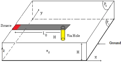
Let’s consider a thin homogeneous dielectric layer between two planes P1 and P2 (Figure 1). A metallic VIA is realized to connect the microstrip line (P1) to the ground (P2). We suppose that all the tangential components (ox and oy directions) of the electric field (or magnetic field or incident wave) are known on P1 and P2, and we would like to calculate the magnetic field (or electric field or reflected wave).
The analysis procedure consists of dividing the electromagnetic field on two components, the TEM mode and its orthogonally ones. The first is the projection of the electromagnetic field onto VIA-hole domain, whereas the second is the projection onto the complementary domain; it is the orthogonal component of the TEM mode where only the TM modes are considered.
Figure 1. Microstrip line with VIA hole.
Metal VIA Hole Dielectric Excitation A1 B1
A2 B2
ε r
A’2 B’2 Plan 1/Circuit
H
Plan 2/Ground
Figure 2. Definition of waves for planar circuit with VIA hole.
The problem is that the projection of a function on another requires the inner product definition. We can hesitate between two representations. The first has the tangential components (ox and oy
directions). This is used on Moment’s Method. The second has the longitudinal components (oz
direction). The longitudinal formulation is extremely important, especially when the circuit includes a metallic via-hole. In this case, the numerical and analytical considerations prove that the longitudinal approach is indispensable to show convincing results with low computing resources.
In a free source medium and assuming thatejωttime depends on the electromagnetic fields E and
H, the four Maxwell’s equations are written as:
rot E = −jωμ H (1a)
rot H = jω E (1b)
div E = 0 (1c)
div H = 0 (1d)
From Maxwell’s equations we find the relationship between the longitudinal and the transverse components. Equation (1c) can be used to find the electric field components from the longitudinal one. Similarly, Equation (1d) provides transverse magnetic field components.
∂xEx+∂yEy = −∂zEz (2a)
∂xHx+∂yHy = −∂zHz (2b) Taking the curl of the electric and magnetic fields (Equations (1a) and (1b)), we get:
∂xEy−∂yEx = −jωμHz (3a)
Equations (2) and (3) express the complete relation between longitudinal and transverse components of the electromagnetic field. For the electric field and in its condensed form, these equations
become:
−∂zEz
−jωμHz
= ˆL Ex Ey
where Lˆ = ∂x ∂y
−∂y ∂x
(4)
In the case of the magnetic field, we define the pseudo-magnetic field ‘J’ which is commonly named Surface Current Density J =H×z. Using Equations (2b) and (3b) and the surface density current,
we obtain.
jωεEz
∂zHz
= ˆL· Jx Jy
, Lˆ has the same definition as (4) (5) Having defined the longitudinal fields, one can deduce the field expressions for the TE and TM modes according to their appropriate definitions (Hz=0 for TM modes andEz= 0 for TE modes). For the electric filed, modes can be calculated using the following set of equations:
eT M = ∂xEx+∂yEy =−∂zEz (6a)
eT E = ∂xEy−∂yEx =−jωμHz (6b) For our analysis, only the TM modes are considered because we assume that the TE modes are not disturbed by the VIA. The TM modes are normal and contain the TEM VIA hole mode. In fact, the TEM mode verifiesrotE = 0 and can be decomposed on the transverse TM modes that constitute a complete base. For the TEM mode, the electric field E and current density J are carried by a unit vector noted V. The TEM component is the projection of the TM onto the unit vector V; it is the extraction of the TEM component from the total TM modes.
Assume that a general TM magnitude ‘MT M(x, y)’ which can be the electric fieldE, current density
J incident wave A or reflected wave B. MT M(x, y) has TEM component and other TM components. The decomposition is calculated using a projector on the VIA hole and with a classical dot product. More details of this procedure are in the next section.
MT M(x, y) =|V(x, y)V(x, y) MT M(x, y)
T EM componet
+ (1− |V(x, y).V(x, y)|) MT M(x, y)
other components
(7)
3. IMPLEMENTATION OF THE LONGITUDINAL WAVE CONCEPT ITERATIVE PROCEDURE (LWCIP)
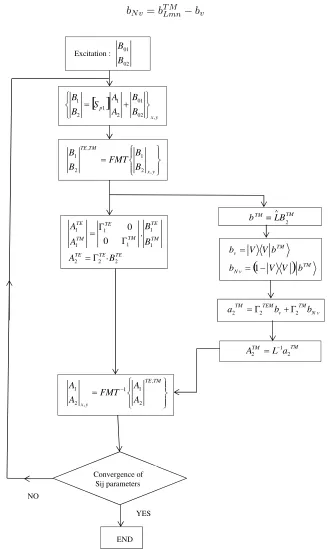
The Wave Concept Iterative Process has been extensively used for wide variety of microwave structures and circuits [8–11]. This iterative process uses waves instead of electromagnetic fields. It consists in successive reflections between the circuit and its two sides. The algorithm uses two equations; one is defined in the spatial domain and describes the waves on the circuit plan, commonly named Spatial Equation St.E., whereas the second is defined in spectral domain and describes waves in the two sides of the circuit plan. The latter is commonly named Spectral Equation Sp.E. Figure 2 is shown for better explanation. This figure shows the relation between waves on each plan. These waves B1(x, y),
B2(x, y),A1(x, y) andA2(x, y) are assumed to be transversal. According to the notification of Figure 2, the spatial and spectral equations will be given by the two following relationships.
St.E. equation:
B1
B2
= [Sp1]
A1
A2
+ B01
B02
(8)
[SP1] is the spatial operator describing the boundaries’ conditions on the circuit, which is the same as [11].
Sp.E. equation:
AT Ei AT Mi
=
ΓT Ei 0 0 ΓT Mi
BiT E BT Mi
‘i’ is the medium index equal to 1 in upper medium and 2 in the lower medium, and ΓT Ei and ΓT Mi are the spectral reflection coefficients for the TE and TM modes, respectively. They depend on the wave guide geometry. For a rectangular waveguide with ‘a’ and ‘b’ dimensions, these coefficients are given by
Γαi =m,n |Fαmn1−z0iY
α i
1 +z0iYiα
Fmnα | (10)
α is the TE or TM modes and z0i the medium impedance.
For rectangular waveguide, the TM and TE modes generator functionFmn∝ are defined as in [11]
FmnT M =
⎧ ⎪ ⎪ ⎪ ⎨ ⎪ ⎪ ⎪ ⎩
Fxmn(xy) =kmnm a ·
2σ2
mn
√
ab ·sin mπx
a cos nπx
b
Fymn(xy) =kmnn b ·
2σ2
mn
√
ab ·cos mπx
a sin nπx
b
(11a)
FmnT E =
⎧ ⎪ ⎪ ⎪ ⎨ ⎪ ⎪ ⎪ ⎩
Fxmn=kmn−n b ·
2σ2
mn
√
ab ·cos mπx
a sin nπx
b
Fymn=kmnm a ·
2σ2
mn
√
ab ·sin mπx
a cos nπx
b
(11b)
wherekmn= 1
(nb)2+(ma)2 and σ 2
mn= 1 if m·n= 0 and equal 2 ifm·n= 0.
YiT E = γ
jωμ0
, YiT M = jωε0
γ andγ
2=mπ
a
2nπ
b
2 −k02
The Fast Mode Transformation (FMT) and its inverse one (F M T−1)) are used to transform waves from spatial to spectral domain and vice versa.
For the upper medium (i = 1), we apply the classic spectral equation Sp.E. for the all modes without any change [12].
{A1 = Γ1B1}T E,T M (12)
In the lower medium (i= 2), the TE mode is non-disturbed by the VIA hole, and then we use the classic equation for these modes.
{A2= Γ2B2}T E (13)
For the TM modes, the expression for longitudinal magnitude is calculated using Equation (6a). Let’s consider the wave B2 outcome of the Equation (8). B2 has two components following (ox) and (oy), respectively. The decomposition ofB2 on the waveguide modes gives.
⎧ ⎨ ⎩
B2xmn(xy) =
mnb2xmnFxmn(xy)
B2ymn(xy)=
mnb2ymnFymn(xy)
(14)
b2xmn andb2ymn are their associate magnitudes.
Using the longitudinal operator Equation (4) we get the TM longitudinal components.
bT ML =
mnb2xmn∂xFxmn(xy) +
mnb2ymn∂yFymn(xy) =
mnb T M
Lmngmn(xy) (15)
wherebT MLmn=kmn(b2xmn+b2ymn) andgmn(xy) =
√ 2σ2mn √
ab sin mπx
a sinnπyb .
Once the longitudinal component is calculated, we proceed to a filtering operation. This filtering operation consists in extracting the VIA modes. Let’s consider ‘V(xy)’ be the normalized indicator filtering function. V(xy) equals √1
Sv on the VIA and zero elsewhere, where the normalization coefficient
‘Sv’ is the VIA surface. The VIA component is the projection on V(xy) whereas its orthogonal one is the remaining. The VIA component is given by the following projection.
Using the expression of the longitudinal wave outcome of Equation (15), one can simplify the bv
expression and get
bV =|V (xy)
V (xy)
mnb T M
Lmngmn(xy)
=
mnb T M
LmnV (xy)|gmn(xy) |V (xy)
(17)
The outside VIA component is the subtraction ofbv from the total longitudinal TM wave.
bN v=bT MLmn−bv (18)
Convergence of Sij parameters END YES NO Excitation : 02 01 B B TE TE TE TM TE TM TE TM TE B A B B A A 2 2 2 1 1 1 1 1 1 . . 0 0 Γ = Γ Γ =
(
)
TMv N TM v b V V b b V V b − = = 1 v N TM v TEM TM b b
a2 =Γ2 +Γ2
TM TM a L A 2 1 2 − = ⎪⎭ ⎪ ⎬ ⎫ ⎪⎩ ⎪ ⎨ ⎧ = − TM TE y x A A FMT A A , 2 1 1 , 2 1
b = LBTM TM
2 ^
[ ]
y x p B B A A S B B , 02 01 2 1 1 2 1 ⎭ ⎬ ⎫ ⎩ ⎨ ⎧ + = ⎪⎭ ⎪ ⎬ ⎫ ⎪⎩ ⎪ ⎨ ⎧ = y x TM TE B B FMT B B , 2 1 , 2 1The last step of this analysis is to make the spectral reflection independently for the two components, then we get
aT M2 = ΓT EM2 bv+ ΓT M2 bN v (19) Consequently, we return to the transverse representation using the longitudinal to transverse transformation (L−1), and the process is repeated until convergence. In this context, a schematic description of the iterative process is illustrated in Figure 3.
4. IV-APPLICATION OF THE LONGITUDINAL APPROACH 4.1. Microstrip Line Ending with a Metallic Via-Hole
The proposed approach is applied at first to study a microstrip line shunted to the ground by a VIA with L0 = 4.6 mm, r = 9.8 and W = H = 0.635 mm (see Figures 1–2). The circuit plan is divided
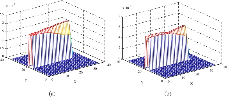
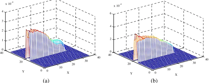
into small cells (see Figure 4). The convergence of the LWCIP process is depicted in Figure 5. For the two states (with and without via hole), the current density behavior is represented in Figures 6 and 7. With via hole, we notice that the current is maximum on via hole for the two frequencies, which models a short-circuit well. The case without via hole is given by the curves in Figure 7. We notice that the current is weak at the end of the line, which models an open circuit.
Figure 4. Mesh of circuit plan with its different sub domains.
0.8 0.85 0.9 0.95 1
50 100 150 200 250 300 350 400
Iterations
S
11
Figure 5. Convergence of LWCIP process as function of iterations number for a microstrip with VIA hole at 2 GHz.
0 10
20 30
40
0 20
40 0 0. 5 1 1. 5 2 2. 5
x 10-3
X
Y 0 10
20 30
40
0 20
40 0 2 4 6 8
x 10-3
X Y
(a) (b)
0 10
20 30
40
0 20 40
0 1 2 3 4
x 10-4
X
Y 0 10
20 30
40
0 20 40
0 2 4 6
x 10-4
X Y
(a) (b)
Figure 7. (a) Current density |Jx|for the open circuit case (without via-hole) at 1 GHz. (b) Current density|Jx|for the open circuit case (without via-hole) at 2 GHz.
In order to validate the longitudinal approach, we make a comparison between our approach and the known analytical formula for the shunt circuit case,
Zin=Z0tan (βL) (20)
Z0 is the characteristic impedance,β the propagation constant andL in the line length.
This comparison concert the response of the input impedance as function the line length. In fact, the line length comprises the microstrip line length (L0) and the VIA-hole length (H). The first component is considered constant whereas second is variable. Figure 8 illustrates this comparison and shows a good agreement for the resonant frequencies. For this simple case, the transverse representation shows a bad results, and the convergence of numerical method (Iterative on wave) is very slow (three thousand iterations), whereas in this approach the convergence is obtained with two hundred iterations [13].
4.2. 2-SIW Slot Antenna
The Substrate Integrated Waveguide consists of two or more rows of metallic VIA created in a dielectric substrate [14, 15]. The VIA diameter ‘d’ and distance D separating two adjacent VIA ‘D’ have been the subject of several studies [16–18]. Then some empirical equations are optimized to calculate these parameters efficiently [19]. In SIW cavity, we assume that only TE modes can propagate. The first resonant frequency corresponds to the T E101 mode. These equations must be respected for the guide that operates as conventional rectangular waveguide.
f101(GHz) =
c
2√μrεr
1
weff
2
+
1
leff
2
(21)
whereweff (mm) =w−0.d952D andleff (mm) =l−0.95d2D.
As we notice, the dielectric height does not intervene in the expression. This parameter is used only to calculate the characteristic impedance of the microstrip line.
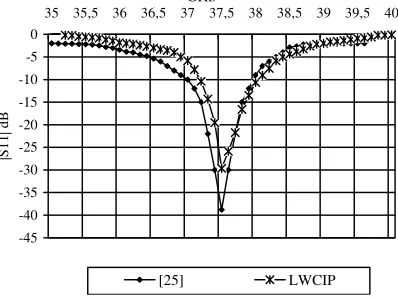
SIW-based slot antenna has been reported in several works [20–24]. In [25], an association of SIW filter and antenna is studied in the MMW frequency range. This technique includes making an aperture on the upper electric wall. In the present work, we use this structure to validate our approach. Figure 9 shows the top view of this structure. The used substrate is Rogers5880 with a relative permittivity of 2.2 and thickness of 0.254 mm. The VIA diameter dequals 0.4 mm, and the distance D between two adjacent VIA is equal to 0.7 mm. The circuit plan parameters are: Wws = 0.78 mm, Lms = 3 mm,
Wtaper = 1.2 mm, Ltaper = 1.2 mm, D1 = 2.4 mm, D2 = 0.6 mm, x = 0.15 mm, w = 0.18 mm,
Lslot= 3.5 mm andWsiw = 4 mm.
___Zc.tan(β (L0+H)) -8
-6 -4 -2 0 2 4 6 8
9,3075 39,3075 69,3075 99,3075 129,3075 L mm
Zin K
Ω
Our Method
Figure 8. Zin us function of Via-hole length L(L=L0+H),L0 = 4.6 mm,f = 2 GHz and εr= 1.
Figure 9. The geometry of the SIW slot antenna.
-45 -40 -35 -30 -25 -20 -15 -10 -5 0
35 35,5 36 36,5 37 37,5 38 38,5 39 39,5 40
GHz
|S11| dB
[25] LWCIP
Figure 10. Return loss as function of frequency.
5. CONCLUSION
REFERENCES
1. Tao, J. W., J. Atechian, R. Ratovondrahata, and H. Baubrand, “Transverse operator of large class of multidielectric waveguides,” IEEE Proc., Vol. 137, 135–139, 1990.
2. Schelkunoff, S. A., “Generalized telegraphist’s equations for waveguides,” Bell. Syst. Tech. J., Vol. 31, 748–801, Jul. 1952.
3. Solano, M. A., A. Prieto, and A. Vegas, “Comparative study of two different formulation of coupled mode theory for analyzing rectangular dielectric waveguide,” Proceedings of the 8th International
Conference on Antennas and Propagation, Vols. 1–2, 45–47, Heriot-Watt University, Edinburgh,
UK, Mar. 30–Apr. 2, 1993.
4. Amalric, J. L., H. Baudrand, and M. Hollinger, “Various aspects of coupled mode theory for anisotropic partially filled waveguide: Application to a semiconductor loaded with perpendicular induction,”7th European Microwave Conference Copenhagen, 146–149, Denmark, Sep. 1977. 5. Preibisch, J. B., A. Hardock, and C. Schuster, “Physics-based via and waveguide models for efficient
SIW simulations in multilayer substrates,”IEEE Trans. Microw. Theory Techn., early access, 2015. 6. Rimolo-Donadio, R., X. Gu, Y. Kwark, M. Ritter, B. Archambeault, F. de Paulis, Y. Zhang, J. Fan, H. Br¨uns, and C. Schuster, “Physics-based via and trace models for efficient link simulation on multilayer structuresup to 40 GHz,”IEEE Trans. Microw. Theory Techn., Vol. 57, No. 8, 2072– 2083, Aug. 2009.
7. Zhang, Y., J. Fan, G. Selli, M. Cocchini, and F. de Paulis, “Analytical evaluation of via-plate capacitance for multilayer printed circuit boards and packages,” IEEE Trans. Microw. Theory
Techn., Vol. 56, No. 9, 2118–2128, Sep. 2008.
8. Hrizi, H., L. Latrach, N. Sboui, A. Gharsallah, A. Gharbi, and H. Baudrand, “Improving the convergence of the wave iterative method by filtering techniques,” Applied Computational
Electromagnetic Society Journal, Vol. 26, No. 10, 2011.
9. Latrach, L., N. Sboui, A. Gharsallah, H. Baudrand, and A. Gharbi, “Analysis and design of planar multilayered fss with arbitrary incidence,”Applied Computational Electromagnetic Society Journal, Vol. 23, No. 2, 149–154, Jun. 2008.
10. Sboui, N., A. Gharsallah, H. Baudrand, and A. Gharbi, “Global modeling of periodic structure in coplanar wave guide,” Microwave and Opt. Techno. Lett., Vol. 43, No. 2, 157–160, Oct. 2004. 11. Sboui, N., A. Gharsallah, H. Baudrand, and A. Gharbi, “Global modeling of microwave active
circuits by an efficient iterative procedure,” IEE Proc. — Microw. Antennas Propag., Vol. 148, No. 3, 209–212, Jun. 2001.
12. Sboui, N., A. Gharsallah, H. Baudrand, and A. Gharbi, “Design and modeling of RF MEMS switch by reducing the number of interfaces,” Microwave and Opt. Techno. Lett., Vol. 49, No. 5, 1166–1170, May 2007.
13. Zairi, H., A. Gharsallah, A. Gharsallah, A. Gharbi, and H. Baudrand, “Modelization of probe feed excitation using iterative method,” Applied Computational Electromagnetic Society Journal, Vol. 19, No. 3, 198–205, Nov. 2004.
14. Yan, L., W. H. K. Wu, and T. J. Cui, “Investigations on the propagation characteristics of the substrate integrated waveguide based on the method of lines,” IEE Proc. — Microw. Antennas
Propag., Vol. 152, 35–42, 2005.
15. Boozzi, M., A. Georgiandis, and K. Wu, “Review of substrate-integrated waveguide circuits and antennas Microwaves,” IET Antennas & Propagation, Vol. 5, No. 8, 909–920, Jun. 6, 2011.
16. Deslandes, D. and K. Wu, “Single-substrate integration technique of planar circuits and waveguide filter,” IEEE Trans. Microw. Theory Techn., Vol. 51, No. 2, 593–596, Feb. 2003.
17. Deslandes, D. and K. Wu, “Design consideration and performance analysis of substrate integrated waveguide components,” 32nd European Microwave Conference, 2002.
18. Mikulasek, T., J. Lacik, and W. Raida, “SIW slot antennas utiliwed for 60 GHz channel characterization,” Microwave and Opt. Techno. Lett., Vol. 57, No. 6, 1365–1370, Jun. 2015. 19. Jian, Z., Y. Yuanwei, Z. Yong, C. Chen, and J. ShiXing, “A high — Q microwave MEMS resonator,”
20. Deslandes, D. and K. Wu, “Accurate modeling wave mechanisms and design considerations of a substrate integrated waveguide,” IEEE Trans. Microw. Theory Techn., Vol. 54, No 6, 2516–2526, Jun. 2006.
21. Zelenchuk, D. and C. Fusco, “Low insertion loss substrate integrated waveguide quasi-elliptic filters for V-band wireless personal area network applications,”IEE Proc. — Microw. Antennas Propag., Vol. 5, No. 8, 921–927, Jun. 6, 2011.
22. Patel, A., Y. Prashad, A. Vala, and R. Goswami, “Design and performance analysis of metallic posts coupled SIW based multiband passband and stopband filter,” Microwave and Opt. Techno.
Lett., Vol. 57, No. 6, 1409–1417, Jun. 2015.
23. Cassivi, Y., L. Perregrini, K. Wu, and G. Conciauro, “Low-cost and high-Q millimeter-wave resonator using substrate integrated waveguide technique,”32nd European Microwave Conference, 1–4, Milan, Italy, Sep. 2002.
24. Cassivi, Y., L. Perregrini, P. Arcioni, M. Bressan K. Wu, and G. Conciauro, “Dispersion characteristics of substrate integrated rectangular waveguide,” IEEE Microwave and Wireless
Components Letters, Vol. 12, No. 9, 333–335, Sep. 2002.