Ground Plane Effect Suppression Method to Design a Low-Profile
Printed UWB Antenna
Aliakbar Dastranj* and Faezeh Bahmanzadeh
Abstract—This paper presents a technique to design a very small planar antenna for ultra-wideband (UWB) communication applications. To cover UWB frequency range by a small-size antenna, the ground plane influence on the antenna impedance bandwidth is suppressed at middle and higher frequencies. To accomplish this purpose, a rectangular and several stepped slots are etched on the conventional radiator. Also, a tuning stub is printed in the rectangular slot, and its length is optimized. This technique decreases current distribution on the ground plane at higher frequencies, and the impedance matching of the antenna is significantly influenced by the radiating patch. The antenna has a compact size of 25×25×1.6 mm3. It can provide a wide impedance bandwidth from 2.8 to 15.4 GHz (|S11| < −10 dB) which covers the entire UWB spectrum (3.1–10.6 GHz). Two prototypes of the
antenna were fabricated and measured. The impedance matching, group delay, fidelity factor, and the antenna radiation characteristics, including co- and cross-polarized far-field patterns and realized gain were analyzed with numerical simulation and experimental measurement. Measured data are in good agreement with the simulated ones. Based on the obtained frequency- and time-domain characteristics, the designed antenna is an excellent candidate for UWB wireless devices.
1. INTRODUCTION
Designing a compact size antenna with the most attractive characteristics such as low complexity, low cost, functioning over an extremely large impedance bandwidth (BW), high data rate, and low interference in the modern wireless-enabled devices is a very challenging task, nowadays [1, 2]. Ultra-wideband (UWB) planar monopole antenna with the allocated frequency spectrum of 3.1–10.6 GHz can be a good candidate to design in such communication systems [3]. However, as the demand for high data transmission is increasing, both short and long range frequency spectra are needed. As UWB technology provides higher data rates and higher and more balanced bandwidth than narrowband systems, it can be used to send data, voice, and video at higher speeds or ranging and monitoring applications, both in civil and military systems [4].
In recent years, to fulfill the UWB communication technology necessities, different structures of planar antennas, including planar monopoles [5–8], planar dipoles [9, 10], and quasi-Yagi configurations [11, 12] have been presented. A planar slot antenna with an overall area of 50 mm×68 mm and impedance bandwidth of 2.08–8.25 GHz was proposed in [13]. In [14], by using a widened tuning stub, a coplanar waveguide (CPW)-fed square slot antenna with a size of 72×72 mm2 featureed a bandwidth of 60%. In [15], by using a U-shaped tuning stub, a UWB mono-layer slot antenna with a thickness of 0.813 mm was proposed. It can provide bidirectional radiation patterns and impedance bandwidth of 110%. The antennas presented in [16] had identical areas of 110×110 mm2 and frequency bandwidths of 120% and 110%. In [17], corners of a slot antenna were shaped to design a multi-resonance structure with a bandwidth of 105.3%. In [18], two bevels were cut on an asymmetrical rectangular
Received 1 November 2019, Accepted 20 December 2019, Scheduled 8 January 2020
* Corresponding author: Aliakbar Dastranj ([email protected]).
92 Dastranj and Bahmanzadeh
patch to improve the impedance bandwidth. By using this technique, an open-slot antenna with a broad impedance bandwidth of 122% was implemented. In [19], a rotated square slot resonator was used to design a parasitic patch antenna with a bandwidth of 2.23–5.36 GHz. A CPW-fed antenna with a half-elliptical-edged radiating patch and double open-circuit stubs for 3.7–10.1 GHz was proposed in [20]. Two mono-layer UWB antennas with sizes of 50×50 mm2 and 48×42 mm2 and operating bandwidths of 125% and 118.8% were reported in [21] and [22], respectively.
In this research, a planar monopole UWB antenna with suppressed ground plane effect is presented. In order to suppress ground plane influence on the antenna impedance bandwidth, a rectangular and several stepped slots are etched on the radiating patch. Furthermore, to reduce the current distribution on the ground plane at a desired frequency, a strip is printed in the rectangular slot. This technique decreases current distribution on the ground plane at higher frequencies. Consequently, the impedance matching of the antenna is mainly affected by the antenna radiator. The designed antenna has a simple configuration with compact size of 25×25×1.6 mm3. It can cover a wide operating bandwidth from 2.8 to 15.4 GHz (|S11|<−10 dB). To validate the proposed technique, the antenna was fabricated, and
comparison between the measured results and simulated ones is presented. Experimental outcomes show good agreement with the numerical data. The frequency- and time-domain results of the antenna including impedance bandwidth, co- and cross-polarized far-field patterns, realized gain, group delay, and fidelity factor are illustrated and discussed.
2. ANTENNA EVOLUTION PROCEDURE AND DESIGN
The evolution procedure, geometrical parameters, and fabricated prototypes of the proposed antenna are shown in Figure 1. It is seen that the final proposed structure contains asymmetric staircase-like radiating patch with modified ground plane. Moreover, a tuning strip with length Ls is printed in the rectangular slot near the left side of the radiator. As will be seen later, the combination of the aforementioned portions results in UWB operating bandwidth. The antenna is printed on an FR4 substrate with permittivity of 4.4 and loss tangent of 0.02. The overall area of the antenna is 25×25 mm2. The numerical analysis and geometry refinement of the proposed structure are performed by using Ansoft HFSS, a full-wave electromagnetic simulator package which is based on the finite element method. Different structures shown in Figure 1(b) were simulated, and their comparison results of reflection coefficient curves are illustrated in Figure 2. The design procedure starts with the design of Antenna1. As shown in Figure 1(b), Antenna1 consists of beveled ground plane and a rectangular radiator which is fed by a 50 Ω microstrip line. Referring to Figure 2, it can be observed that Antenna1 provides a
−10-dB reflection coefficient bandwidth from 11.5 to 15.5 GHz. After etching an open ended inverted L-shaped slot on the left portion of the radiating patch, impedance matching of the antenna at 6 GHz is slightly improved. In the next step, several staircase-like slots are etched on three corners of the radiator (Antenna3), and as depicted in Figure 2, Antenna3 exhibits a resonance in the reflection coefficient at 7.7 GHz whereas Antenna2 does not. However, the lower band edge frequency of Antenna3 is 3.2 GHz which cannot satisfy the requirement for UWB systems. Afterwards, a strip with lengthLs and width of 1 mm is printed in the rectangular slot near the left side of the radiator (Antenna4). As illustrated in Figure 2, the lower band edge frequency of the operating bandwidth is shifted from 3.2 to 2.8 GHz. Also, the second resonance frequency of the antenna and the higher end of the operating bandwidth occur at 12 and 15 GHz, respectively. As a result, Antenna4 can cover the broad frequency range of 2.8–15 GHz. In the last step of the antenna design, the fourth corner of the radiator is stepped to further enhance the impedance bandwidth of the antenna. As illustrated in Figure 2, the proposed antenna features good impedance matching over the entire frequency range of 2.8–15.4 GHz. Its impedance bandwidth is more than 138% for|S11|<−10 dB. Although the final optimized design is based on full-wave HFSS
simulations, simple formulas can be derived to provide an initial design and insight. The initial length of the strip can be calculated approximately from the following equation:
Ls= 1.92×fC
r× √εeff
(a)
(b)
Figure 1. (a) Fabricated prototypes of the antenna, (b) antenna evolution procedure and geometry.
94 Dastranj and Bahmanzadeh
Figure 3. Surface current distribution on the antenna.
whereCis the speed of light in free space;fr is the desired resonance frequency; andεeff is the effective dielectric constant and can be approximated by:
εeff = εr + 1
2 +
εr−1 2
1
1 + 12d/w
(2)
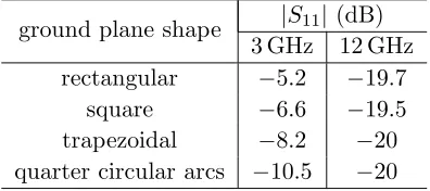
wheredis the thickness of substrate, andwis the width of common microstrip line. Is should be pointed out that in Eq. (2), εeff is the effective relative permittivity of common microstrip line. Although the strip of length Ls is not exactly the case of common microstrip line, the approximate value of Ls in Eq. (1) can serve as a starting point to calculate the length of strip from which it can be optimized to obtain a final value. By using Eq. (1), the initial value ofLsis 8 mm forfr = 12 GHz. However, the final optimized value for maximum impedance bandwidth is 7 mm. The surface current distribution on the antenna radiator and ground plane at 3 and 12 GHz is presented in Figure 3. It is seen that the current distribution at the lower frequency, 3 GHz, is considerably concentrated on the ground plane, while at the higher frequency, 12 GHz, current distribution is mainly concentrated on the staircase-like radiator and attached strip. This shows that the proposed technique considerably reduces the influence of the ground plane on the antenna impedance bandwidth at higher frequencies. To better justify this point, the reflection coefficients of the proposed antenna with different ground plane shapes are tabulated in Table 1. As can be seen, the low frequency performance of the proposed antenna depends on the ground plane shape, but at higher frequencies the ground plane does not affect the antenna reflection coefficient. The evolution procedure discussed above clearly shows that the staircase-like radiating patch with modified ground plane and attached strip jointly provide the UWB performance of the antenna.
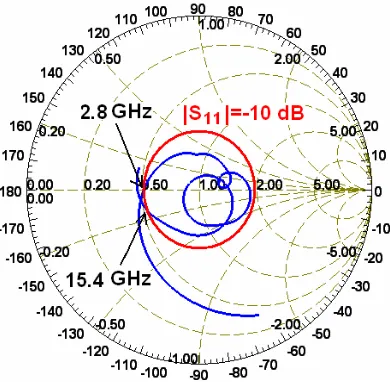
To furthered study the impedance matching of the designed structure, the simulated input impedance on Smith chart of the antenna is plotted in Figure 4. This figure shows two loops on the Smith chart, which are related to two resonant frequencies illustrated on the reflection coefficient plot of Figure 2. Moreover, it can be observed that these loops are completely inside the|S11|=−10 dB
circle, and the proposed antenna has a simulated −10-dB impedance bandwidth ranging from 2.8 to 15.4 GHz.
At last, a numerical sensitivity analysis was performed to find the influence of important design
Table 1. Reflection coefficient of the antenna with different ground plane structures.
ground plane shape |S11|(dB)
3 GHz 12 GHz
rectangular −5.2 −19.7
square −6.6 −19.5
trapezoidal −8.2 −20
Figure 4. Input impedance Smith chart of the antenna.
(a) (b)
Figure 5. Reflection coefficient curves for different values ofLs and Ds. (a)Ls, (b)Ds.
parameters on the performance of the antenna. It was found that strip length,Ls, and distance between the microstrip feed-line and open ended inverted L-shaped slot on the left portion of the radiating patch, Ds, have considerable influence on the UWB performance of the proposed antenna. Figure 5(a) shows the influence of strip length Ls on the reflection coefficient of the antenna while the other geometrical parameters are unchanged. As can be observed, this parameter affects the antenna reflection coefficient over the entire UWB spectrum. Figure 5(b) shows the simulated reflection coefficient curves for different values ofDswhile other geometrical parameters are kept fixed. As depicted in this figure, the reflection coefficients at middle and higher frequencies largely depend onDs. However, this parameter does not affect the lower band edge frequency of the antenna. Figure 5 shows that selecting the optimal values of Ls= 7 mm and Ds= 4.3 mm leads to maximum impedance bandwidth.
3. EXPERIMENTAL VERIFICATION AND DISCUSSION
Figure 1(a) shows a photograph of the proposed antenna prototypes. The antenna was simulated by using HFSS software package. Then, it was fabricated to validate the results obtained by simulation. The designed antenna is connected to a 50 Ω SMA connector for signal transmission.
96 Dastranj and Bahmanzadeh
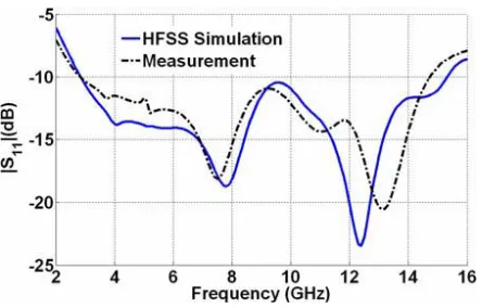
Figure 6. Comparison between the numerical and experimental reflection coefficient curves of the antenna.
(|S11|<−10 dB) which covers the entire UWB spectrum (3.1–10.6 GHz). There is a difference between
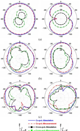
the experimental and numerical results due to measurement and also fabricating errors. However, in order to further understand the utility of the proposed antenna over the entire operating bandwidth, other radiation characteristics such as far-field patterns and realized gain must also be carefully investigated. Far-field radiation patterns of the proposed UWB antenna at 3, 9, and 15 GHz in H (x-z)- and E (y-z)-planes are plotted in Figure 7. As can be observed from Figure 7(a), the antenna has an omnidirectional pattern inH-plane and bidirectional pattern inE-plane at low frequencies with low cross polarization level. Figures 7(b) and 7(c) show that the radiation patters at middle and higher frequencies are also reasonable. The distortion of radiation pattern at high frequencies is due to the asymmetric structure of radiator and attached strip. As mentioned in Section 2, at the higher frequencies current distribution is mainly concentrated on the staircase-like radiator and attached strip, while the current distribution at the lower frequencies is considerably concentrated on the symmetric ground plane. Notice that the cross polarization level increases at higher frequencies due to excitation of higher order modes. Figure 8 illustrates the simulated three-dimensional radiation pattern of the antenna at 3 GHz. As expected from a monopole structure, it features omnidirectional and bidirectional patterns in x-z- and y-z-planes respectively. The simulated and measured gain curves of the antenna versus frequency are illustrated in Figure 9. The maximum value of the measured antenna gain is 4.4 dBi which occurs at 13 GHz. It is seen that the measured gain is moderate at the operating frequency band due to the small size (25×25 mm2) and omnidirectional behavior of the antenna. Although not shown, the gain in other directions is acceptable.
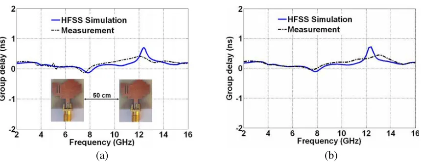
Along with frequency-domain analysis, time-domain performance should also be analyzed in order to be sure of the UWB operation. The time-domain analysis required two identical designed antennas, one as the transmitter and the other as a receiver, in the adjustment of face-to-face and side-by-side. Time-domain analysis of both configurations was considered using CST Microwave Studio by a distance of 50 cm. Time taken by the antenna to receive the pulse is indicated by an important parameter named group delay. The simulated and experimental group delays of face-to-face and side-by-side orientations are shown in Figure 10 in which the peak-to-peak variation is less than 1 ns over the entire frequency band. Results of group delay indicate that the antenna provides an excellent time-domain performance without signal distortion.
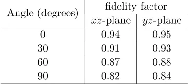
Another important parameter in time-domain analysis named fidelity factor is used to calculate the correlation between transmitted and received pulses. According to the procedure proposed in [23], the input signal is delivered to the antenna, and the far-field electric component is received by means of four virtual probes. To investigate the fidelity factor in bothE- and H-planes, four probes are placed at the angle equal toθ= 0◦, 30◦, 60◦, and 90◦ (with respect to positive z-axis) iny-z- andx-z-planes, respectively. In the numerical simulation procedure, the input signal was defined by a fourth-order Rayleigh pulse as follows:
st=
12 τ2 −
48 τ6(t−1)
2+16
τ8(t−1) 4 exp − t−1
τ 2
(a)
(b)
(c)
Figure 7. Experimental and numerical far-field E (y-z)- and H (x-z)-plane patterns of the antenna (left: x-z plane, right: y-z plane) at (a) 3 GHz, (b) 9 GHz, and (c) 15 GHz.
with τ = 67 ps. According to [24], the fidelity factor, F F, for the received pulse was calculated as follows:
F F = max k
∞
−∞
¯
98 Dastranj and Bahmanzadeh
Figure 8. 3D radiation pattern of the antenna at 3 GHz.
Figure 9. Gain of the antenna versus frequency.
(a) (b)
Figure 10. Comparison between the experimental and numerical group delay results of the antenna versus frequency. (a) Side-by-side, (b) face-to-face.
Table 2. Calculated fidelity factor of the antenna.
Angle (degrees) fidelity factor xz-plane yz-plane
0 0.94 0.95
30 0.91 0.93
60 0.87 0.88
90 0.82 0.84
mentioned in [24], a fidelity factor higher than 50% is an appropriate value for UWB systems. Table 2 presents this time-domain parameter for both planes. It is seen that the calculated fidelity factors in both planes have proper values above 82%, making the proposed antenna very capable for use in UWB communication applications. To calculateF F, as mentioned in [24], the antenna gain andE-field phase should be calculated at every angle of the desired plane. Using the aforementioned parameters and transfer function of two identical antennas, like the procedure proposed in [24], the cross-correlation between the received and transmitted pulses is done at every point in time, and the maximum value of this correlation is obtained. The F F in Eq. (4) has to be solved for every angle and plotted in a polar plot. Because of the normalization of the signals, the results of the cross-correlation are between 0 and 1.
4. CONCLUSION
A printed monopole UWB antenna with suppressed ground plane effect has been presented in this work. To suppress ground plane effect on the antenna impedance bandwidth, a rectangular and several stepped slots are etched on the radiating patch. Besides, to reduce the current distribution on the ground plane at a desired frequency, a strip is printed in the rectangular slot. This technique decreases current distribution on the ground plane at higher frequencies. Consequently, the impedance matching of the antenna is mainly affected by the antenna radiator. The antenna has a compact size of 25×25×1.6 mm3. It can provide a wide impedance bandwidth from 2.8 to 15.4 GHz (|S11|< −10 dB) which covers the
entire UWB spectrum. Two prototypes of the antenna were fabricated and measured. The impedance matching, group delay, fidelity factor, and antenna radiation characteristics, including co- and cross-polarized far-field patterns and realized gain were analyzed with numerical simulation and experimental measurement. Measured data are in good agreement with the simulated results. Based on the obtained frequency- and time-domain characteristics, the designed antenna is an attractive candidate for UWB wireless devices.
REFERENCES
1. Pfeiffer, C., T. Steffen, and G. Kakas, “Uniform beamwidth UWB feed antenna using lossy transmission lines,” Progress In Electromagnetics Research, Vol. 165, 119–130, 2019.
2. Raad, H. K., “An UWB antenna array for flexible IoT wireless systems,” Progress In Electromagnetics Research, Vol. 162, 109–121, 2018.
3. Ahmed, O. and A. R. Sebak, “A printed monopole antenna with two steps and a circular slot for UWB applications,” IEEE Antennas Wirel. Propag. Lett., Vol. 7, 411–413, 2008.
4. Oraizi, H. and S. Hedayati, “Miniaturized UWB monopole microstrip antenna design by the combination of Giusepe Peano and Sierpinski carpet fractals,” IEEE Antennas Wirel. Propag. Lett., Vol. 10, 67–70, 2011.
100 Dastranj and Bahmanzadeh
6. Abbosh, A. M. and M. E. Bialkowsky, “Design of ultrawideband planar monopole antennas of circular and elliptical shape,”IEEE Trans. Antennas Propag., Vol. 56, No. 1, 17–23, 2008.
7. Koohestani, M. and M. Golpour, “U-shaped microstrip patch antenna with novel parasitic tuning stubs for ultra wideband applications,” IET Microw. Antennas Propag., Vol. 4, No. 7, 938–946, 2010.
8. Eldek, A. A., A. Z. Elsherbeni, and C. E. Smith, “Wide-band modified printed bow-tie antenna with single and dual polarization for C- and X-band applications,”IEEE Trans. Antennas Propag., Vol. 53, No. 9, 3067–3072, 2005.
9. Chen, G.-Y. and J.-S. Sun, “A printed dipole antenna with microstrip tapered balun,” Microw. Opt. Technol. Lett., Vol. 40, No. 4, 344–346, 2004.
10. Zheng, G., A. A. Kishk, A. B. Yakovlev, and A. W. Glisson, “Simplified feed for a modified printed Yagi antenna,”Electron. Lett., Vol. 40, No. 8, 464–466, 2004.
11. Kaneda, N., W. Deal, Y. Qian, R. Waterhouse, and T. Itoh, “A broad-band planar quasi-Yagi antenna,” IEEE Trans. Antennas Propag., Vol. 50, No. 8, 1158–1160, 2002.
12. Deal, W., N. Kaneda, J. Sor, Y. Qian, and T. Itoh, “A new quasi-Yagi antenna for planar active antenna arrays,”IEEE Trans. Microwave Theory Tech., Vol. 48, No. 6, 910–918, 2000.
13. Lee, H. L., H. J. Lee, J. G. Yook, and H. K. Park, “Broadband planar antenna having round corner rectangular wide slot,”Proc. IEEE Antennas and Propagation Society Int. Symp., Vol. 2, 460–463, Jun. 16–21, 2002.
14. Chen, H.-D., “Broadband CPW-fed square slot antennas with a widened tuning stub,”IEEE Trans. Antennas Propag., Vol. 51, No. 4, 1982–1986, Aug. 2003.
15. Chair, R., A. A. Kishk, and K. F. Lee, “Ultrawideband coplanar waveguide-fed rectangular slot antenna,” IEEE Antennas Wirel. Propag. Lett., Vol. 3, 227–229, 2004.
16. Liu, Y. F., K. L. Lau, Q. Xue, and C. H. Chan, “Experimental studies of printed wide-slot antenna for wide-band applications,” IEEE Antennas Wirel. Propag. Lett., Vol. 3, 273–275, 2004.
17. Eskandari, H., M. R. Booket, M. Kamyab, and M. Veysi, “Investigation on a class of wideband printed slot antenna,” IEEE Antennas Wirel. Propag. Lett., Vol. 9, 1221–1224, 2010.
18. Liu, W. X., Y. Z. Yin, W. L. Xu, and S. L. Zuo, “Compact open-slot antenna with bandwidth enhancement,”IEEE Antennas Wirel. Propag. Lett., Vol. 10, 850–1224, 2011.
19. Sung, Y., “Bandwidth enhancement of a microstrip line-fed printed wide-slot antenna with a parasitic center patch,” IEEE Trans. Antennas Propag., Vol. 60, No. 4, 1712–1716, Apr. 2012. 20. Xu, K., Z. Zhu, H. Li, J. Huangfu, C. Li, and L. Ran, “A printed single-layer UWB monopole
antenna with extended ground plane stubs,” IEEE Antennas Wirel. Propag. Lett., Vol. 12, 237– 240, 2013.
21. Siddiqui, J. Y., C. Saha, and Y. M. M. Antar, “A novel ultrawideband (UWB) printed antenna with a dual complementary characteristic,”IEEE Antennas Wirel. Propag. Lett., Vol. 14, 974–977, 2015.
22. Unnikrishnan, D., D. Kaddour, S. Tedjini, E. Bihar, and M. Saadaoui, “CPW-fed inkjet printed UWB antenna on ABS-PC for integration in molded interconnect devices technology,” IEEE Antennas Wirel. Propag. Lett., Vol. 14, 1124–1128, 2015.
23. Wu, Q., R. Jin, J. Geng, and M. Ding, “Pulse preserving capabilities of printed circular disk monopole antennas with different grounds for the specified input signal forms,” IEEE Trans. Antennas Propag., Vol. 55, No. 10, 2866–2873, Oct. 2007.