78:3 (2016) 293–300 | www.jurnalteknologi.utm.my | eISSN 2180–3722 |
Jurnal
Teknologi
Full Paper
T
HEORETICAL
S
TUDY ON
S
LOW
-
LIGHT
G
ENERATED BY
I
NTEGRATED
M
ICRORING
R
ESONATOR WITH
W
IDE
B
ANDWIDTH AND
H
IGH
G
AIN
M. S. Aziz
*, M. S. Affandi, S. Daud, M. Bahadoran, K. T. Chaudhary,
J. Ali
Laser Center, Ibnu Sina Institute for Scientific and Industrial Research
(ISI-SIR) Universiti Teknologi Malaysia, 81310 UTM Johor Bahru, Johor,
Malaysia
Article history
Received
15 August 2015
Received in revised form
15 November 2015
Accepted
30 December 2015
*Corresponding author
[email protected]
Graphical abstract
Abstract
We proposed a new approach to generate slow light transmission with large bandwidth and high buildup factor by using a soliton pulse propagating within integrated ring resonator circuit. The system consisted series of micron-size ring resonator fabricated by using nonlinear InGaAsP/InP material that are laterally coupled together. For convenience of analysis, optical transfer function for this model is obtained by using z-transform method. Slow light performances were modeled and discuss in this paper. Intensity buildup induced within the series of rings located at left and right sides of the system while strong nonlinear Kerr effect and mutual coupling leads to the spreading frequency bands within the device. Numerical simulation verifies that signal pulse with 45 ps relative delay time and bandwidth of 5.9 GHz (47 pm) are obtained at the communication wavelength around 1550 nm for a 100 ps signal pulse.
Keywords: Nonlinear optics, fibers, coupled resonators, slow-light
Abstrak
Kami mencadangkan pendekatan baru untuk menjana cahaya perlahan dengan jalur lebar yang besar dan faktor tokokan tinggi dengan menggunakan denyut soliton merambat dalam litar bersepadu cincin resonator. Sistem ini terdiri dariada siri cincin resonator bersaiz mikron direka dengan menggunakan bahan tak linear InGaAsP / InP yang dicantumkan secara sisipan. Untuk kemudahan analisis, fungsi pemindahan optik untuk model ini diperolehi dengan menggunakan kaedah z-transform. Prestasi cahaya perlahan dimodelkan dan dibincangkan dalam manuskrip ini. Intensiti tokokan terhasil dalam siri cincin yang terletak di kiri dan kanan sistem manakala kesan tak linear Kerr dan gandingan bersama membawa kepada rebakan jalur frekuensi dalam peranti. Simulasi berangka mengesahkan bahawa nadi isyarat dengan 45 ps masa tunda relatif dan lebar jalur 5.9 GHz (47 pm) diperolehi pada panjang gelombang komunikasi sekitar 1.550 nm untuk isyarat denyut 100 ps.
Kata kunci: Optik tak-linear, fiber, pengalun bercantum, cahaya perlahan
1.0 INTRODUCTION
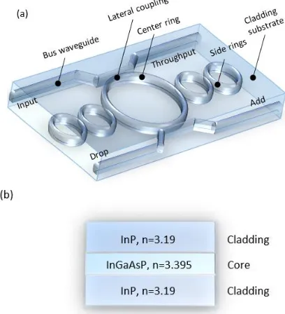
In recent years, slow light technologies have become one of the most important research topic with much of the studies focusing on development of technique that has the ability to control the transmission delay of optical signals [1, 2]. This technique offers wide range of potential applications in signal processing such as optical buffer [3], optical delay lines [4, 5] and quantum information [6]. Among all the approaches in realization of slow light, integrated optical waveguide platform is more promising due to its strong optical confinement and easy integration with ultra-compact photonics circuit [7, 8]. Recent studies have shown that strong mutual coupling in integrated multi-coupled ring resonator system induced resonant splitting that leads to pulse advancement or delay with relatively low distortion in signal pulse [9]. For instant, a number of theoretical and experimental works on generation of slow light have been demonstrated [10, 11]. Technically, the use of ring resonator device requires a high degree of control especially in all-optical signal processing system. However, the fundamental of single ring resonator system only provide simple Lorentzian response [12]. Due to this matter, some configuration is not suitable for many important applications in dense wavelength division multiplexing (DWDM) systems. Therefore, tailoring the filter response shape is needed in order to enhance the potential application of ring resonator in various field of studies. For this purpose, specific design of microring resonator (MRR) device consisting one center ring coupled to a series of microrings on the left and right hand side of the system is considered as shown in Figure 1. This unique configuration is known as “double-PANDA” ring resonator device. Optical transfer function of such system is first derived by implementing z-transform method to the photonics circuit accordingly. To date, different approaches have been used in order to determine the signal transfer function of integrated MRR system including transfer matrix method [13-17], Vernier principle [18-21] and signal flow graph method [22, 23]. In this study, a novel attempt has been made in order to achieve a delay light transmission within the proposed system with relatively large bandwidth and high buildup factor. The whole research works might contribute towards the new perspective on realization of slow light.
2.0 OPERATING PRINCIPLE
Operating system of double PANDA ring resonator is shown in Figure 1. The system consisted of one center ring, two straight waveguides and four side-rings. The straight waveguides are coupled on top and bottom of the center ring, while all side-rings are arranged in particular configuration such that two rings are serially coupled on both lateral sides of the center ring by using 2x2 optical directional coupler. This
configuration consisted of four main ports. Optical signals are injected into the system through input and add ports while the corresponding signals are ejected from the system through throughput and drop ports respectively.
Figure 1 (a) Double PANDA ring resonator configuration and (b) layer structure of composed system
3.0 PHOTONICS TRANSFER FUNCTION
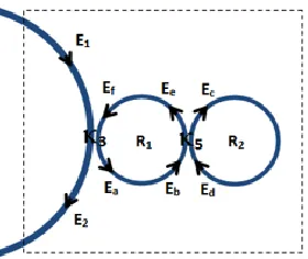
Referring to the schematic diagram of double PANDA ring resonator system as depicted in Figure 2, Input signals Ein and Eadd are injected into the system
through input and add ports. Meanwhile, output signals Et and Ed are ejected from the system via
throughput and drop ports. Circulating fields associated with different points on the center ring are denoted as E0, E1, E2, E3, E4, E5, E6and E7. i represents
the coupling factor for ith optical directional coupler
connecting ring resonator and the bus waveguide. Fraction of light that continues to propagate in its original direction is called the transmission coefficient and it is given by 𝑦𝑖= √1 −𝑖. Vice versa, the other
fraction which travels across the waveguide (coupled to the second waveguide) is called cross-coupling coefficient denoted by 𝑗√ [24, 25]. Transmission for
one complete roundtrip of light propagation in ring resonator is derived using z-transform method and given it is by ξ=ɑz^(-1) [26]. The term ɑ is assigned as the total loss coefficient of the ring waveguide for one complete roundtrip and it is given by ɑ=exp〖((-αL)⁄2) 〗where α refers to attenuation loss constant. Noted
that if we assume that ring resonator is ideal with no losses, then the value of ɑ is unity. z-transform parameter is represented by〖 z〗^(-1)=〖exp〗^(-jk_n L)
to the phase propagation of field passing through the ring resonator system [27].
Figure 2 Schematic diagram of Double PANDA ring resonator
As shown in Figure 2, 1 and 2 are the coupler
parameters for the coupling between center ring and the straight waveguides while 3, 4, 5and 6 are the
coupler parameters for the coupling between the rings respectively. Radius of the center ring is denoted as R while R1, R2, R3 and R4 are the ring radiuses for the
side-rings on the left and right sides of the center ring. To obtain the optical transfer function of this system, new set of parameters are used for simplification purpose which are 𝑦1= √1 −1, 𝑦2= √1 −2, 𝑦3= √1 −3, 𝑦4= √1 −4, 𝑦5= √1 −5, 𝑦6= √1 −6 and 𝑥1= √1 − 𝛾1, 𝑥2= √1 − 𝛾2, 𝑥3= √1 − 𝛾3, 𝑥4= √1 − 𝛾4, 𝑥5= √1 − 𝛾5 , 𝑥6= √1 − 𝛾6 where γiis the ith intensity
insertion loss coefficients for six different coupler of the system. By taking into account the coupling coefficient and insertion loss coefficient for each coupler, throughput and drop port signals can be expressed by:
𝐸𝑡= 𝑥1𝑦1𝐸𝑖𝑛+ 𝑗𝑥1√
1𝐸7 (1) 𝐸𝑑= 𝑥2𝑦2𝐸𝑎𝑑𝑑+ 𝑗𝑥2√2
𝐸3 (2)Figure 3 Schematic diagram of right rings on double PANDA ring resonator configuration
For further simplification, new set of parameters are assigned as ϕ=-αL/2-jk_n L,〖 ϕ〗_R1=-(αL_R1)/2-jk_n L_R1,
ϕ_R2=-(αL_R2)/2-jk_n L_R2, ϕ_R3=-(αL_R3)/2-jk_n L_R3 and ϕ_R4=-(αL_R4)/2-jk_n L_R4 which indicate the transmission of light after passing through one complete roundtrip for each corresponding ring. To obtain the analytical transfer function of this system, let first consider the right-hand side part of the circuit containing R1 and R2. By using z-transform method, circulating fields on the right rings as shown in schematic diagram in Figure 3 are expressed by:
𝐸𝑎= 𝑗𝑥3√
3𝐸1+ 𝑥3𝑦3𝐸𝑓 (3) 𝐸𝑏= 𝐸𝑎exp (𝜙𝑅1
2 ) (4)
𝐸𝑐= 𝑗𝑥5√
5𝐸𝑏+ 𝑥5𝑦5𝐸𝑑 (5) 𝐸𝑑= 𝐸𝑐exp(𝜙𝑅2) (6) 𝐸𝑒= 𝑗𝑥5√
5𝐸𝑑+ 𝑥5𝑦5𝐸𝑏 (7) 𝐸𝑓= 𝐸𝑒exp (𝜙𝑅1
2 ) (8)
Simplifying these equations yield:
𝐸𝑎= 𝐴𝐸1 (9)
Where
𝐴 = 𝑗𝑥3√3
1−𝑥3𝑦3[𝑥5𝑦5−𝑥52 exp(𝜙𝑅2)
1−𝑥5𝑦5 exp(𝜙𝑅2)] exp(𝜙𝑅1)
(10)
Expression above describes the relation of Ea in term of the input signal E1. Similarly, expressions for the other components of circulating fields in term of E1 can be written as:
𝐸𝑏 = [exp ( 𝜙𝑅1
2 )] 𝐴𝐸1 (11)
𝐸𝑐 = [
𝑗𝑥5√5exp(𝜙𝑅12 )
1−𝑥5𝑦5exp(𝜙𝑅2)] 𝐴𝐸1 (12)
𝐸𝑑= [
𝑗𝑥5√5exp(𝜙𝑅12 ) exp(𝜙𝑅2)
1−𝑥5𝑦5exp(𝜙𝑅2) ] 𝐴𝐸1 (13)
𝐸𝑒= [
𝑥5𝑦5−𝑥52exp(𝜙𝑅2)
1−𝑥5𝑦5exp(𝜙𝑅2)] 𝐴𝐸1exp ( 𝜙𝑅1
2 ) (14) 𝐸𝑓 = [
𝑥5𝑦5−𝑥52exp(𝜙𝑅2)
According to the diagram, circulating field on the center ring E2 can be expressed by:
𝐸2= 𝑥3𝑦3𝐸1+ 𝑗𝑥3√
3𝐸𝑓 (16)Substituting Eq. (15) into Eq. (16) yields:
𝐸2= [𝑥3𝑦3−
𝑥323𝑒𝑥𝑝(𝜙𝑅1)[𝑥5𝑦5−𝑥52𝑒𝑥𝑝(𝜙𝑅2)]
1−𝑥5𝑦5𝑒𝑥𝑝(𝜙𝑅2)−𝑥3𝑦3𝑒𝑥𝑝(𝜙𝑅1)[𝑥5𝑦5−𝑥52𝑒𝑥𝑝(𝜙𝑅2)]] 𝐸1
(17) For simplification, C12 is assigned as:
𝐶12= 𝑥3𝑦3−
𝑥323𝑒𝑥𝑝(𝜙𝑅1)[𝑥5𝑦5−𝑥52𝑒𝑥𝑝(𝜙𝑅2)]
1−𝑥5𝑦5𝑒𝑥𝑝(𝜙𝑅2)−𝑥3𝑦3𝑒𝑥𝑝(𝜙𝑅1)[𝑥5𝑦5−𝑥52𝑒𝑥𝑝(𝜙𝑅2)]
(18) Finally, expression for E2 in term of E1 can be written
as:
𝐸2= 𝐶12𝐸1 (19)
Similarly for the left-hand-side part of the circuit as shown in Figure 4, expression for E6 in term of E5 can be
written as:
𝐸6= 𝐶34𝐸5 (20)
Where
𝐶34= 𝑥4𝑦4−
𝑥424𝑒𝑥𝑝(𝜙𝑅3)[𝑥6𝑦6−𝑥62𝑒𝑥𝑝(𝜙𝑅4)]
1−𝑥6𝑦6𝑒𝑥𝑝(𝜙𝑅4)−𝑥4𝑦4𝑒𝑥𝑝(𝜙𝑅3)[𝑥6𝑦6−𝑥62𝑒𝑥𝑝(𝜙𝑅4)]
(21)
Figure 4 Schematic diagram of left rings on double PANDA ring resonator configuration
Referring back to Figure 2, relations between circulating fields of the system can be written as:
𝐸0= 𝑗𝑥1√
1𝐸𝑖𝑛+ 𝑥1𝑦1𝐸7 (22) 𝐸1= 𝐸0exp (𝜙𝑅
4) (23) 𝐸2= 𝐶12𝐸1 (24) 𝐸3= 𝐸2exp (
𝜙𝑅
4) (25) 𝐸4= 𝑗𝑥2√
2𝐸𝑎𝑑𝑑+ 𝑥2𝑦2𝐸3 (26) 𝐸5= 𝐸4exp (𝜙𝑅
4) (27) 𝐸6= 𝐶34𝐸5 (28) 𝐸7= 𝐸6exp (
𝜙𝑅
4) (29)
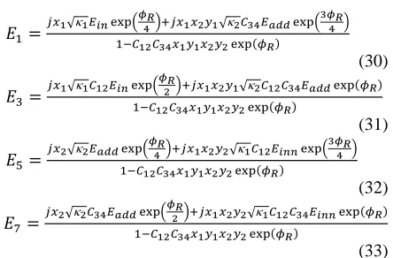
By using these sets of equations, the terms E1, E3, E5 and E7 can be expressed as:
𝐸1=
𝑗𝑥1√1𝐸𝑖𝑛exp(𝜙𝑅4)+𝑗𝑥1𝑥2𝑦1√2𝐶34𝐸𝑎𝑑𝑑exp(3𝜙𝑅4 )
1−𝐶12𝐶34𝑥1𝑦1𝑥2𝑦2exp(𝜙𝑅)
(30)
𝐸3=
𝑗𝑥1√1𝐶12𝐸𝑖𝑛exp(𝜙𝑅2)+𝑗𝑥1𝑥2𝑦1√2𝐶12𝐶34𝐸𝑎𝑑𝑑exp(𝜙𝑅)
1−𝐶12𝐶34𝑥1𝑦1𝑥2𝑦2exp(𝜙𝑅)
(31)
𝐸5=
𝑗𝑥2√2𝐸𝑎𝑑𝑑exp(𝜙𝑅4)+𝑗𝑥1𝑥2𝑦2√1𝐶12𝐸𝑖𝑛𝑛exp(3𝜙𝑅4 )
1−𝐶12𝐶34𝑥1𝑦1𝑥2𝑦2exp(𝜙𝑅)
(32)
𝐸7=
𝑗𝑥2√2𝐶34𝐸𝑎𝑑𝑑exp(𝜙𝑅2)+𝑗𝑥1𝑥2𝑦2√1𝐶12𝐶34𝐸𝑖𝑛𝑛exp(𝜙𝑅)
1−𝐶12𝐶34𝑥1𝑦1𝑥2𝑦2exp(𝜙𝑅)
(33)
Referring back to Eqs. (1) and (2), and by using the sets of equations above, finally expressions for Et and Ed the can be written as:
𝐸𝑡= 𝑥1𝑦1𝐸𝑖𝑛+ 𝑗𝑥1√
1𝐶34𝐸5exp ( 𝜙𝑅4) (34) 𝐸𝑑= 𝑥2𝑦2𝐸𝑎𝑑𝑑+ 𝑗𝑥2√
2𝐶12𝐸1exp (𝜙𝑅
4) (35) Eqs. (34) and (35) give the expressions for throughput and drop port signals in term of only Ein and Eadd. The expressions clearly provide direct relation between input and output signals and thus it can be used as the transfer function of double PANDA ring resonator system.
4.0 NUMERICAL APPROACH
In this section, transmission properties of optical signals going across nonlinear fiber ring resonator are modelled by using iterative method. Sequences of improving approximate solutions for serially-coupled double ring resonators integrated on both sides of system are generated accordingly. By using Eqs. (3-8) that have been derived earlier, Ef can be expressed as:
𝐸𝑓 = [
1−𝑥5𝑦5exp(𝜙𝑅2)
𝑥5𝑦5−exp(𝜙𝑅2)] 𝐸𝑎 (36)
Eq. (36) describes the relation between circulating field Ef in term of only Ea. Generally, amplitudes of the electric fields inside the right ring at the n¬th roundtrips are given as:
𝐸𝑎(1) = 𝑗𝑥3√
3
𝐸1 (37) 𝐸𝑓(𝑛 + 1) = [1−𝑥5𝑦5𝑒𝑥𝑝(𝜙𝑅2)
𝑥5𝑦5−𝑒𝑥𝑝(𝜙𝑅2)] 𝐸𝑎(𝑛 + 1) (38)
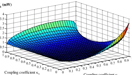
Figure 5 Peak power at throughput port, It plotted against κ1 and κ2 in 3 dimensions for double PANDA configuration
These sets of equations describe the expressions for the circulating and output fields for n number of roundtrip made within the right ring resonator. The term Ea (1) represents the first portion of light coupled into the ring waveguide and it correspond to the first roundtrip of light going across the ring. The field Ef is always one complete roundtrip ahead of Ea as can be seen from the schematic diagram. Due to the symmetrical geometry of PANDA ring resonator system, similar expressions for the left ring can be expressed as:
𝐸𝑔(1) = 𝑗𝑥4√
4𝐸5 (41) 𝐸𝑙(𝑛 + 1) = [1−𝑥6𝑦6𝑒𝑥𝑝(𝜙𝑅4)
𝑥6𝑦6−𝑒𝑥𝑝(𝜙𝑅4)] 𝐸𝑔(𝑛 + 1) (42)
𝐸𝑔(𝑛 + 1) = 𝑗𝑥4√
4𝐸5+ 𝑥4𝑦4𝐸𝑙(𝑛 + 1) (43) 𝐸6(𝑛 + 1) = 𝑥4𝑦4𝐸5+ 𝑗𝑥4√4
𝐸𝑙(𝑛 + 1) (44)5.0 RESULTS AND DISCUSSION
First, basic transmission of double PANDA configuration are simulated and discussed in this section. Output signals ejected from throughput and drop ports are governed by sets of equations that have been first derived in Equations (34) and (35). The mathematical relations suggested that both output power at throughput, It and drop port, Id are extremely
dependent on the coupling parameters of first and second coupler on the center ring. Results are generated based on the system with center ring radius of R=50 μm and side ring radiuses of R1=R2=R3=R4=10
μm respectively. Coupling coefficients κ3, κ4, κ5 and κ6
are fixed at 0.30. Some relations were examined by plotting 3-dimensional graph. During simulation process, input power is set at 1 mW and coupling coefficients values were varied from 0 to 1.
Figure 5 shows the relation between output signals at throughput port and coupling coefficient κ1 and κ2. From the graph, we can see that It reach the highest value at specific point where κ1 is equal to one while κ2 is zero. Referring to the geometry of double PANDA configuration, as value of κ1 increased, more fraction
of input light Iin are coupled into the ring. This process induces the increasing in the power within the resonator system due to intensity buildup. At the same
being ejected from the system through the second coupler. Technically, all the circulated fields within the ring will be ejected out through the first coupler and this process directly increased the output power at throughput port which corresponds to It with the highest buildup factor recorded at 3.57. The graph also shows that when κ1 is kept at zero value, output power of It does not changed for any value of κ2. This process occurred because there is no fraction of light from input Iin being coupled into the resonator system as κ1=0, thus the transmission coefficient is now equals to unity and this explains why It is having the same value as the initial input.
Figure 6 shows the simulation result of Id plotted against coupling coefficients κ1 and κ2 in 3 dimensions. For the output signals at the drop port, maximum power was recorded at the point where κ1=0 and κ2=1 respectively. Highest buildup factor was calculated at 3.87. Dynamical behaviors of the generated output signals are demonstrated as the peak power of both It and Id varied at different points on the plane as shown in simulation results.
Figure 6 Peak power at drop port, Id plotted against κ1 and κ2 in 3 dimensions for double PANDA configuration
In Figure 7, peak power of the output signal produced at drop-port of double PANDA system is plotted against coupling coefficients κ5 and κ6. Radiuses of the rings are R=50 μm and R1=R2=R3=R4=10 μm. Values of κ1 and κ2 are fixed at 0.1 and 0.35 while κ3 and κ4 are kept at constant value of 0.35 respectively. Both variable parameters κ5 and κ6 are varied from 0 to 1 and the corresponding 3-dimensional result is shown in the Figure 7.
0 0.1 0.2
0.3 0.4 0.5 0.6
0.7 0.8 0.9 1
0 0.1 0.2 0.3 0.4 0.5 0.6 0.7 0.8 0.9 10 0.5 1 1.5 2 2.5 3 3.5 4
Coupling coefficient 1
Coupling coefficient 2 It (mW)
0 0.1 0.2
0.3 0.4 0.5 0.6
0.7 0.8 0.9 1
0 0.1 0.2 0.3 0.4 0.5 0.6 0.7 0.8 0.9 1 0 0.5 1 1.5 2 2.5 3 3.5 4
Coupling coefficient 1
Figure 7 Peak power of the output signal recorded at drop port of double PANDA ring resonator system with respect to coupling coefficients κ5 and κ6
Based on the 3-dimensional result, any increment in the value of κ5 and κ6 will result in greater peak power of Id signal. Highest possible output power of this system is achieved when both coupling coefficient values is unity as clearly shown. Thus, it is said that greater values of both κ5 and κ6 are required to optimize the output signals. In the case where both coupling coefficients are set at zero, there is no component of light from the first ring being coupled into the second ring on either sides of the configuration. Technically, intensity buildup process only occurred in the first ring. In the other words, the outer rings on both sides are neglected in this particular case, which leads to a lower output power recorded at 1.86 mW. This phenomenon shows that the additional rings that are serially coupled on both sides of the system introduce additional intensity buildup on circulated field components. This process results in greater output power as the signal being ejected and collected at throughput and drop port of the system. In this case, mathematical expression that describes the ratio between output and input fields is obtained from Equations (30) to (35):
𝐸𝑡
𝐸𝑖=
𝑦1−𝑦1𝑦2𝑎1𝑒−𝑗𝜙1−𝑦2𝑎1𝑒−𝑗𝜙1+𝑎1𝑒−𝑗𝜙1𝑎2𝑒−𝑗𝜙2
1−𝑦2𝑎2𝑒−𝑗𝜙2−𝑦1𝑦2𝑎1𝑒−𝑗𝜙1+𝑦1𝑎1𝑒−𝑗𝜙1𝑎2𝑒−𝑗𝜙2
(45)
Buildup factor for this configuration, B is given by squared modulus of Equation (45). This system is assumed to be lossless such that attenuation coefficient is unity for both ring (a1=a2=1). For simplification purposes, we assumed that both ring are having the same size where L1=L2 such that ϕ1=ϕ2=ϕ.
To simplify the model further, coupling coefficients are defined as κ1= κ2= κ. By substituting 𝑡 = √1 −
, we can write:𝐵 = 2𝑡2+2𝑡3+𝑡4−2𝑡3cos 𝜙+4𝑡2cos 𝜙+2𝑡 cos 2𝜙−2𝑡 cos 𝜙 1+2𝑡2+2𝑡3+𝑡4−2𝑡 cos 2𝜙−4𝑡2cos 𝜙+2𝑡 cos 𝜙−2𝑡3cos 𝜙 (46)
Considering a system under resonant condition, the terms cos(ϕ) andcos(2ϕ) is equal to unity. Buildup
factor can be written in simplest form as:
𝐵 =6𝑡2+𝑡4
(1−𝑡2)2 (47)
For the convenience of discussion, we consider a system with coupling coefficient values of κ=0.7. Calculation shows that the ratio between output and input intensities of this system is equal to 13.82 at resonant. It is clearly shown that buildup factor for this configuration is significantly high due to the buildup of intensity process that occur within the optical resonating system.
Input signal in the form of bright soliton pulse centered at the communication wavelength around 1550 nm and full-width at half maximum (FWHM) around 100 ps is considered in this section. Initial signal’s power is 2 mW while radiuses of the center and sides ring are fixed at 50 μm and 10 μm respectively. The ring waveguide cross sectional area is 0.50 μm2. The attenuation loss is 10 dB/mm around 1550 nm and intensity insertion loss γ=0.1 respectively [28]. Effective refractive index neff is 3.169 while the intensity-dependent index coefficient n2 of InGaAsP/InP waveguide is 1.76×10⁻¹² cm2/W [29]. For further
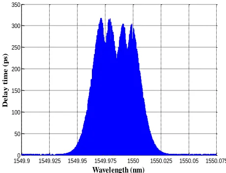
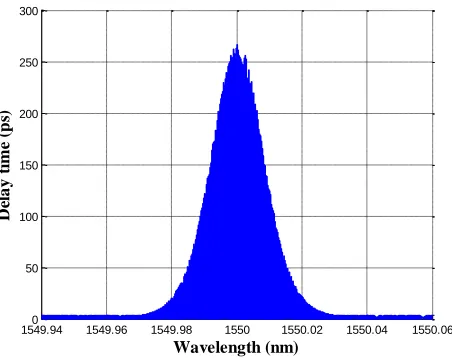
analysis, delay characteristic of output signals ejected from the proposed system are investigated numerically. For comparison purposes, time delay spectrum for light pulse in double PANDA and single ring (SRR) system were calculated and demonstrated as in Figures 8 and 9.
Figure 8 Time delay spectrum for light pulse in double PANDA system
0 0.2
0.4 0.6
0.8 1
0 0.2 0.4 0.6 0.8 1 1 2 3 4 5 6
Coupling coefficient 5 Coupling coefficient 6
I
d (mW)
1549.90 1549.925 1549.95 1549.975 1550 1550.025 1550.05 1550.075 50
100 150 200 250 300 350
Wavelength (nm)
D
e
la
y
t
im
e
(
p
s
Figure 9 Time delay spectrum for light pulse in SRR system
For SRR system, group time delay was recorded around 261 ps with effective bandwidth of 25 pm corresponding to the wavelength of 1550 nm. On the other hand, maximum group time delay for double PANDA system was recorded at 315 ps while bandwidth approaches 47 pm. Large different of group velocity in the entire signal bandwidth induced resonance splitting centered at 1549.97, 1549.98, 1549.99 and 1550 nm that can be observed from the multiple peaks in the light spectrum as clearly shown in Figure 8. This phenomenon arises due to the strong mutual-coupling and time delay contributed from the series of ring resonators coupled on the side of center ring respectively. As demonstrated in Figure 10, group time delay for a pulse propagating in double PANDA system is significantly increased with a noticeable broader 3-dB bandwidth. This phenomenon can be explained by taking into consideration the dispersive effect induced in optical waveguide that are being coupled to a series of optical resonator. During propagation, group velocity of light pulse is significantly reduced due to its effective circulation in each ring resonator before it pass through the structure. Phase shift acquired by interacting light pulse is greatly dependent on its detuning from cavity resonance. In addition, nonlinear response (Self Phase Modulation) from the interaction of light pulse with nonlinear ring resonator produces additional phase shift. Thus, this structure introduces a large dispersive effect which leads to group time delay and bandwidth modification of light pulse.
Figure 10 Time delay spectrum for light pulse in double PANDA and SRR systems
Figure 11 shows the temporal profile of signal pulse after experiencing slow-light propagation through SRR and double PANDA system. Signals delay between the two pulses are about 45 ps. Interacting signals experienced buildup of intensity as it effectively circulate within the series of additional rings coupled on the left and right sides of center ring. Buildup factor is recorded around 2.5 for this set-up. Bandwidth modulation of the signal introduces a broader spectral width and simultaneously producing shorter pulse width. As shown in Figure 11, pulse width decreases from 100 ps to 60 ps. However, output signal is assumed to maintain its soliton shape even with the shorter pulse width. The time bandwidth product (TBP) of output pulse is measured around 0.35, which is slightly greater than the value of the transform limit of sech2 shape pulse. Thus, for pulse propagation within double PANDA system, signal delay is achieved with noticeable signals gain and minor distortion as illustrated.
Figure 11 Temporal profile of signal pulses through double PANDA and SRR system
1549.940 1549.96 1549.98 1550 1550.02 1550.04 1550.06 50
100 150 200 250 300
Wavelength (nm)
D
el
a
y
t
im
e
(p
s)
1549.90 1549.925 1549.95 1549.975 1550 1550.025 1550.05 1550.075 50
100 150 200 250 300 350
Wavelength (nm)
D
e
la
y
t
im
e
(
p
s
)
50 100 150 200 250 300 350 400 450 500
0 0.5 1 1.5 2 2.5 3 3.5 4 4.5 5
Time (ps)
O
u
tp
u
t
P
o
w
e
r
(
m
W)
6.0 CONCLUSION
Based on z-transform method, analytical expression of proposed double PANDA ring resonator configuration is derived including its optical transfer function. By numerical simulation, group time delay of signal passing through the system are obtained near communication wavelength of 1550 nm. By comparing this particular system to SRR, slow light time delay for double PANDA system increased to 315 ps with effective bandwidth recorded around 47 pm. Resonance splitting is observed due to the mutual coupling and nonlinear response. Maximum pulse delay time is recorded at 45 ps with noticeable signal gain and buildup factor recorded around 2.5. Output signal is simulated with pulse width around 60 ps with observable minor signal distortion. TBP for this signal is calculated around 0.35. To summarize, the proposed system can be used to obtain a delay pulse with broader bandwidth and relatively high buildup factor. This technique provides a new setup to realizing slow light in ultra-compact photonics circuit.
Acknowledgement
Authors sincerely thank the support of the Laser Center (UTM) for providing research facilities required to complete this study. The authors gratefully acknowledge the financial support via research of Grant No. QJ130000.2709.01K76.
References
[1] Robert W. Boyd. 2009. Slow and Fast Light: Fundamentals And Applications. Journal of Modern Optics. 56:18-19. [2] Zhao, Y., Zhao, H., Zhang, X., Yuan, B., Zhang, S. 2009. New
Mechanisms Of Slow Light And Their Applications. Optics &
Laser Technology. 41: 517-525.
[3] Suwanpayak N., Jalil M. A., Aziz M. S., Ali J., Yupapin P. P. 2011. Molecular Buffer Using A PANDA Ring Resonator For Drug Delivery Use. International Journal Of Nanomedicine. 6: 575-580.
[4] Han, X., Zhang, J., Song, H., Wang, L., Teng, J., Wu, P., Zhao, M. 2013. Influence Of Coupling Conditions On The Time Delay Characteristics Of Parallel-Cascaded Optical Waveguide Ring Resonators. Optik - International Journal
for Light and Electron Optics. 124: 377-384.
[5] Liu, H. and Yariv, A. 2012. Ideal Optical Delay Lines Based On Tailored-Coupling And Reflecting, Coupled-Resonator Optical Waveguides. Opt. Lett. 37:1964-1966.
[6] Parra, E. and Lowell, J. 2007. Toward Applications of Slow Light Technology. Opt. Photon. News. 18: 40-45.
[7] Xia, F., Sekaric, L. and Vlasov, Y. 2007. Ultracompact Optical Buffers On A Silicon Chip. Nature Photonics. 1: 65-71
[8] Varmazyari, V., Habibiyan, H. and Ghafoorifard, H. 2013. All-optical Tunable Slow Light Achievement In Photonic Crystal Coupled-Cavity Waveguides. Appl. Opt. 52: 6497-6505. [9] Li, Q., Zhang, Z., Wang, J., Qiu, M. and Su, Y. 2009. Fast Light
In Silicon Ring Resonator With Resonance-Splitting. Opt.
Express. 17: 933-940
[10] Zadok, A., Eyal, A. and Tur, M. 2011. Stimulated Brillouin Scattering Slow Light In Optical Fibers. Appl. Opt. 50: 38-49. [11] Lee, M., Zhu, Y., Gauthier, D., Gehm, M. and Neifeld, M. 2011. Information-theoretic Analysis Of A
Stimulated-Brillouin-Scattering-Based Slow-Light System. Appl. Opt. 50: 6063-6072.
[12] Saeung, P., and Yupapin, P. P. 2008. Generalized Analysis Of Multiple Ring Resonator Filters: Modeling By Using Graphical Approach. Optik - International Journal for Light
and Electron Optics. 119: 465-472.
[13] Tsay, A. and Van, V. 2012. Analysis of Coupled Microring Resonators in Sheared Lattices. Photonics Technology
Letters, IEEE. 24: 1625-1627
[14] Dey, S., Mandal, S. S. 2013. Wide Free-Spectral-Range Triple Ring Resonator As Optical Filter. Opt. Eng. 50: 2920-2927. [15] Fan, G., Li, Y., Liu, X. and Zhen, Z. 2012. The Optimum Design
Model Of Two Resonators System. Optics & Laser
Technology. 44: 825-829
[16] Aziz, M. S., Jalil, M. A., Suwanpayak, N., Ali, J. and Yupapin, P. P. 2012. Optical Manipulation Of Nano-Micro Needle Array For Large Volume Molecular Diagnosis. Artificial Cells,
Blood Substitutes, and Biotechnology. 40(4): 266-270
[17] Tsay, A. and Van, V. 2011. Analytic Theory of Strongly-Coupled Microring Resonator. IEEE Journal of Quantum
Electronics. 47: 997-1005
[18] Dey, S. B., Mandal, S. and Jana, N. N. 2011. Quadruple Optical Ring Resonator Based Filter On Silicon-On-Insulator.
Optik - International Journal for Light and Electron Optics.
124: 2920-2927.
[19] Sirawattananon, C., Bahadoran, M., Ali, J., Mitatha, S. and Yupapin, P.P. 2012. Analytical Vernier Effects of a PANDA Ring Resonator for Microforce Sensing Application. IEEE
Transactions on Nanotechnology. 11: 707-712.
[20] Dey, S. and Mandal, S. 2012. Modeling And Analysis Of Quadruple Optical Ring Resonator Performance As Optical Filter Using Vernier Principle. Optics Communications. 285: 439-446.
[21] Aziz, M. S., Daud, S., Bahadoran, M., Ali, J. and Yupapin, P.P. 2012. Light Pulse In A Modified Add-Drop Optical Filter For Optical Tweezers Generation. Journal of Nonlinear Optical
Physics and Materials. 21(4): 1250047.
[22] Yupapin, P.P., Saeung, P. and Li, C. 2007. Characteristics of Complementary Ring-Resonator Add/Drop Filters Modeling By Using Graphical Approach. Optics Communications. 272: 81-86.
[23] Aziz, M. S., Bahadoran, M., Noorden, A. F. A., Chaudhary, K., Ali, J. and Yupapin, P. 2015. Analytical Treatment and Modeling of Integrated Ring Resonator Device by Z-Transform Method for Signals Amplification. J. Comput.
Theor. Nanosci. 12: 2253-2258.
[24] Poon, J. K. S., Scheuer, J., Mookherjea, S., Paloczi, G. T., Huang, Y., Yariv, A. 2004. Matrix Analysis Of Microring Coupled-Resonator Optical Waveguides. Optics Express.
12: 90-103.
[25] Aziz, M. S., Suwanpayak, N., Jalil, M. A., Jomtarak, R., Saktioto, T., Ali, J. and Yupapin, P. P. 2012. Gold Nanoparticle Trapping And Delivery For Therapeutic Applications. International Journal of Nanomedicine. 7: 11-17.
[26] Zhang, J., Guo, S. and Li, X. 2013. Independently Tunable Optical Notch Filter Based On Double Ring Resonator Structure. Optik - International Journal for Light and Electron
Optics. 124: 1307-1310.
[27] Pornsuwancharoen, N., Ali, J. and Yupapin, P.P. 2009.
Optical Solitons in Nonlinear Micro Ring Resonators:
Unexpected Results and Applications. Nova Science Pub.
[28] Shimizu, H. and Nakano, Y. 2006. Fabrication And Characterization of an InGaAsP/InP Active Waveguide Optical Isolator With 14.7 dB/mm TE Mode Nonreciprocal Attenuation. Lightwave Technology, Journal of. 24: 38-43. [29] Seo, J. and Mizumoto, T. 2004. Measurement Of Nonlinear Index Changes In An InGaAsP/InP Waveguide Using An Optical Loop Mirror Interferometer. Conference on Lasers and Electro-Optics/International Quantum Electronics
Conference and Photonic Applications Systems
Technologies, Technical Digest (CD) (Optical Society of