Differential Voltage Current Conveyor Based
Clockwise and Counter Clockwise -Hysteresis
Mode Bistable Multivibrator Implementation
Amit Bhattacharyya
Assistant Professor, Department of Electronics and Communication Engineering, Haldia Institute of Technology,
Haldia, India
ABSTRACT: This paper presents a Dual hysteresis mode Flip-flop multivibrator circuit, which is composed of only one Differential voltage current conveyor (DVCC) as the active element. Projected Dual hysteresis mode Flip-flop multivibrator Circuit consists of a DVCC, two resistors R1 and R2, and a double pole double throw dual in- line package (DPDT DIP) mechanical type switch. Top and bottom saturation levels of the Flip-flop multivibrator can be set using passive components. Real structure in design of projected model describes operation of the circuit Is-Spice is the simulation software to simulate the model. Commercially available ICs AD844AN and passive elements are required for circuit implementation. Effectivity of the projected circuit is examined as measured and simulation results well agree with hypothetical result. Simulation and measurement results of Vo–Vin transfer characteristic curves for clockwise and counter clockwise mode with an operating frequency of f=1 kHz are shown. It is observed that the threshold voltages for the simulation and measurement results are close to the design values VTH=5 V, VTL= -5 V, and the projected flip-flop multivibrator circuit is capable of fulfilling the dual hysteresis operation within the same design criteria.
KEYWORDS: Differential voltage current conveyor, Flip-flop multivibrator, clockwise and counter clockwise hysteresis approach, Current conveyor, Positive feedback.
I. INTRODUCTION
Table 1. Comparisons between different Flip-Flop multivibrator structures
STRUCTURE ELEMENTS PASSIVE
ELEMENT S TYPE
ELECTRO NICALLY ADJUSTA
BLE
HYSTERES IS PROCEDU
RE
MAXIMUM OPERATING FREQUENCY
Operational amplifier build-in
[1]Operational amplifier =1 [2] Resistor = 2
Atleast one earthed
No Single Tens of KHz
Second generation current conveyor (CCII)
[1] CCII = 1
[2] Resistor = 3
Atleast one earthed
No Single Hundreds of
KHz
Differential voltage current conveyor (DVCC)
[1] DVCC =1 [2] Resistor = 2
[3] DPDT DIP switch = 1
Atleast one earthed
Yes Dual Hundreds of
KHz
Aspects of the projected models are as follows:
Quantity of devices applies to propose design is more or less same.
Resistors are shorted to ground to achieve benefits of Integrated Circuit manufacturing procedures. Achieved functioning frequency is greater compare to Operational Amplifier constructed design. Using same topology uniqueness of dual hysteresis operation is obtained.
Possibility of variation with temperature is fewer.
Relevancy of entirely DVCC constructed design enhances. Higher and lower threshold voltages are electronically adjustable.
In Section 2, basic concept and construction of DVCC is emphasized. Then working ideology of bistable multivibrator model is described and associated expressions are given. Also non-ideality and parasitic properties of the planned circuit is analyzed in third Section .In fourth Section, a useful fabrication technique and parametric criteria is introduced. Later, laboratory examinations are performed on the fabricated model. Operation of planned model is checked via simulation software and laboratory examination results. Programme and laboratory examined outputs match with hypothetical concepts. Last portion consists of conclusion.
II. CIRCUITDELIBERATIONSANDFUNCTIONINGPRINCIPLE
A. PRIMARY CONCEPT AND IMPLEMENTATION OF DVCC
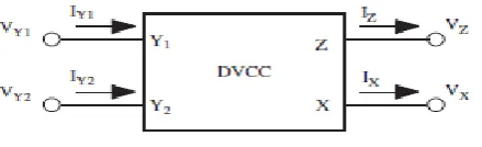
DVCC is suitable in continuous signal processing areas due to its large input resistance voltage terminals and large output resistance current terminals. Circuit symbol of DVCC with four terminals is shown in Figure 1.
Fig. 1. Circuit symbol of DVCC
X terminal voltage drop (VX) shows the variance of two Y terminals voltage drops, VY1 and VY2, and X and Z terminal
current propagation,IX and IZ occurs in the same manner. DVCC has zero X terminal input impedance and infinite
impedances at two Y terminals; hence IY1 and IY2 both are zero. Voltage drop at Z terminal is denoted as VZ .From
VX 𝐼𝑌1 𝐼𝑌2 𝐼𝑍 =
0 1 −1 0
0 0 0 0
0 0 0 0
1 0 0 0
𝐼𝑋 𝑉𝑌1 𝑉𝑌2 𝑉𝑍 (1)
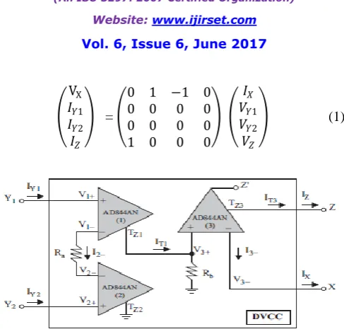
Fig. 2. Implementation of DVCC using IC844AN
Figure 2. demonstrates a hands-on assembly of DVCC consuming simply available ICAD844AN. AD844AN is a special type of OPA due to virtually short inverting and non-inverting inputs. Current propagation through inverting terminal and TZ terminal of AD844AN occurs in the same manner. Due to presence of very high impedance at
Non-inverting input terminals of the first two AD844ANs which results IY1 and IY2 equivalent to zero. Connection between
Tz terminal and non-inverting terminal of first and third IC AD844ANs via grounded resistor Rb provides the variance
of two Y terminals voltage drops,VY1 and VY2, and X and Z terminal current propagation,IX and IZ occurs in the same
manner. Figure 2. depicts the following relationships between voltage and current:
1 11
V
V
V
Y (2)
2 22
V
V
V
Y (3)0
2 1
Y
Y
I
I
(4) a Y Y a TIR
V
V
R
V
V
I
I
1 2 1 22
(5)
Z T
X
I
I
I
I
3
3
(6))
(
1 21 3
3 Y Y
a b b T
X
V
V
R
R
R
I
V
V
V
(7)
V3+ and V3- are non-inverting and inverting voltage drop of third ICAD844AN, IT1 is current flowing through TZ
terminal of first ICAD844AN. Therefore, by adjusting resistors Ra=Rb, V-I relationship of idyllic DVCC is achieved.
B. Proposed DVCC Based Model Discussions
Figure 3. depicts projected DVCC-based flip-flop multivibrator consists of a DVCC, two resistors R1 and R2, and a
DPDT DIP mechanical type switch. An oscillator [8] supplies triangular waveform as input signal Vin. Positive
feedback [9] in projected model is obtained by connecting Y1–Z in conjunction with shorted to ground impedance R2 .
Fig. 3. DVCC-based flip-flop multivibrator controlled by switch
Figure 4 (a) shows Vo-Vin transfer characteristics of the projected model during Clockwise (CW) mode operation where
terminals 1 and 3 and terminals 2 and 4 of DPDT DIP switch are shorted. For this mode, equations of current flowing through X and Z terminal Ix and Iz can be written as:
1
R
V
V
I
O inX
(8)2 R V
I O
Z (9) At first output voltage Vo is at upper saturation level Vo+ and input signal Vin is absent in the circuit, that is Vin=0. Let
R1 is smaller than R2. From equation (8) and (9), it is clear that current IX will be higher than IZ. Thus, Vo remains at
top saturation level Vo+ from starting. When input signal Vin is applied in the circuit current IX diminishes gradually
and Vo switches from Vo+ to bottom saturation level Vo- as shown in path 1 of Figure 4 (a). When input signal Vin
diminishes from zero, current IX increases until IX is larger than IZ. Then, Vo switches from Vo- to Vo+ as shown in
path 2 of Figure 4 (a).
Thus, lower and higher threshold voltages, VTL and VTH, can be obtained for the situation when IX=IZ. Expressions of
VTH and VTL in CW mode are given in equation (10) and (11):
) 1 (
2 1 R R V
VTH O (10)
) 1 (
2 1 R R V VTL O
(11)
Fig. 4 (a). Vo–Vin transfer nature of DVCC-based flip-flop multivibrator controlled by switch for CW manner approach
Figure 4 (b) shows VO-Vin transfer characteristics of the projected model during Counter Clockwise (CCW) mode
operation where terminals 1 and 4 and terminals 2 and 3 of DPDT DIP switch are shorted. For this mode, equations of Ix and Iz can be written as:
2 R
V V
I O in
Z
1 R V
I O
X (13)
Fig. 4 (b).Vo–Vin transfer nature of DVCC-based flip-flop multivibrator controlled by switch for CCW manner approach
Let resistor R1 is smaller than R2. From (12) and (13), it is clear that current IX will be higher than IZ. Thus, Vo remains
at the top saturation level Vo+ from starting refer to path 1’ of Figure 4 (b). When input signal Vin diminishes from zero,
current IZ increases. Once IZ is larger than IX, Vo switches from Vo +
to Vo-. Hence lower threshold voltage VTL is
obtained. In path 2’, Vin is lower than VTH and Vo is at Vo-. Once IZ is more negative than IX, output level switches from
Vo- to Vo+. Hence upper threshold voltage VTH is obtained. Expressions of VTH and VTL in CCW mode derived from
(12) and (13) are given in (14) and (15):
) 1 (
1 2
R R V
VTH O (14)
) 1 (
1 2
R R V VTL O
(15)
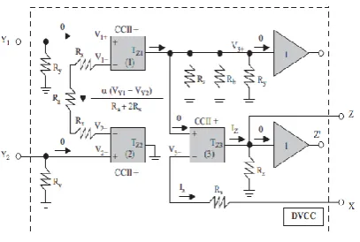
III.REALANDPARASITICPROPERTIESEXPLANATIONS
Using IC AD844AN [10] Second generation current conveyor in positive mode cascaded with buffering voltage having inbuilt parasitic impedances is obtained according to the datasheet. Several non-idealities, like parasitic impedances and real gain concepts are emphasized here. A real structure of used DVCC based circuit model in Figure 5, is given where Rx, Ry, and Rz acting as terminal parasitic resistances. Parasitic resistance Rx is approximately several tens of ohms, but Ry and Rz are approximately several mega-ohms. α is considered as non-ideal voltage gain. According to the datasheet of AD844AN the typical data of α gain = 0.99, β gain =0.98, Rx=50Ω, Ry=10 M Ω, and Rz=3MΩ are considered.
IV.FABRICATIONCRITERIAANDEXAMINEDOUTPUTS
A. Fabrication Techniques and Parametric Criteria
Minimization of the chance of parasitic and real gain effects of the proposed model, the criteria that Ra>>2Rx, R1>>Rx, Rb<< (Rz//Ry), R2<< (Rz//Ry) must be maintained in the fabrication techniques. Parasitic resistance Rx is
approximately several tens of ohms, but Ry and Rz are approximately several mega-ohm range.
Thus the chosen values for resistors R
a, Rb, R1, and R2 range from few kilo-ohms to few hundreds of kilo-ohms.Fabrication criteria are such that R1 must be smaller than R2. DVCC fabricated with easily accessible ICs is able to rise
above the issue of loading effect even in the absence of voltage buffer. For implementation and checking purpose, easily accessible ICs AD844AN and passive components are used to check viability of projected model.
B. Simulated and Examined Outputs
Laboratory examination is performed by using easily accessible AD844AN ICs, two resistors and a DPDT DIP mechanical type switch to obtain projected design. To simulate real structure as given in Figure 5 Spice is the simulation software. Supply voltages of ±15 V with saturation levels Vo+= Vo-= 14 V is maintained for circuit simulations and experiments. External function generator provides applied triggering signal Vtrg. According to the
datasheet of AD844AN the typical data of α gain = 0.99, β gain =0.98, Rx=50Ω, Ry=10 M Ω, and Rz=3MΩ are considered to satisfy the conditions: Rb=10 k Ω <<Rz/Ry=2.3 M Ω and Ra=9.4 k Ω<< 2Rx=100 Ω. During Clockwise
mode operation, the lower and higher threshold voltages are considered as VTH=5 V and VTL= -5 V. Hence, a resistance
ratio[11] of R1/R2=0.64 is achieved. Arbitrarily R2 is considered as 20 k Ω (R2=20 kΩ <<Rz||Ry=2.3 M Ω), and hence
R1 as 12.8 k Ω (R1=12.8 k Ω >>Rx=50 Ω). For counter clockwise mode operation, a resistance ratio R2/R1=1.35 is
chosen, depending upon the said design techniques. Thus, R2 is considered as 20 k Ω (R2=20 kΩ <<Rz||Ry=2.3 M Ω),
and hence R1 as 14.8 k Ω (R1=14.8 k Ω >>Rx=50 Ω).
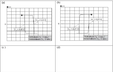
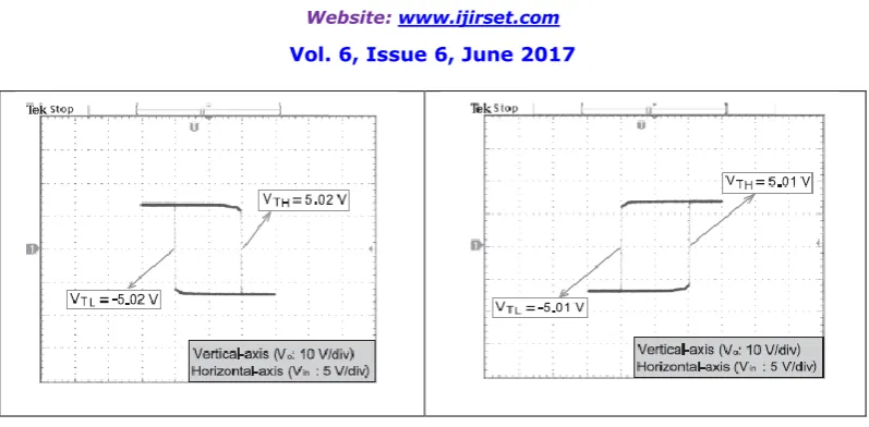
Figure 6(a)-(d) shows the simulation and measurement results of Vo–Vin transfer characteristic curves for CW and CCW mode operations with an operating frequency of f=1 kHz. From Figure 6(a)-(d), it is shown that the threshold voltages for the simulation and measurement results are close to the design values VTH=5 V, VTL= -5 V, and the
projected flip-flop multivibrator circuit is capable of fulfilling the dual hysteresis operation within the same design criteria.
(a) (b)
Fig. 6.Transfer characteristic with an operating frequency of f=1 kHz (a) Simulation result for Clockwise mode (b) Simulation result for Counter Clockwise mode (c) Measurement result for Clockwise mode(d) Measurement result for Counter Clockwise mode
V. CONCLUSION
In this paper, the projected bistable multivibrator model consists of only one DVCCand three resistors and one DPDT DIP mechanical switch. The projected flip-flop multivibrator circuit is able to fulfill the dual hysteresis action surrounded by alike design criteria. Effectiveness of recommended design is scrutinized due to satisfactory results of programme and experiment with theoretical results. The expected design affords new presentation for the DVCC founded systems. DVCC has extensive presentations in the area of communication systems, signal processing field specially processing of electrocardiogram signal [12-13] (ECG), instrumentation, and measurement systems.
REFERENCES
[1] A. Sedra, G. W. Roberts and F. Gohh, “The current conveyor: history, progress and new results,” Proc. IEE Circuits, Devices and Systems, Vol. 137, No. 2, pp. 78–87, 1990.
[2] G. Ferri and N. C. Guerrini, “Low-Voltage Low-Power CMOS Current Conveyors,” Cluwer Academic Publishers,vol. 13, no.9, pp. 1200– 1212, 2003.
[3] B. Dalibor, R. Senani, V. B. and Z. Kolka, “Active elements for analog signal processing: classification, review, and new proposals,” Radio
engineering, Vol. 17, No. 4, pp. 15-32, 2008.
[4] C. Toumazou, F. J. Lidgey and D. G. Haigh, “Analogue IC Design: The current mode approach,” IEEE Circuits and Systems Series 2, Peter Peregrinus, London, 1990.
[5] M. S. Ansari and S. A. Rahman, “A novel current-mode non-linear feedback neural circuit for solving linear equations,” Proc. Int’l Conf. on Multimedia, Signal Processing and Communication Technologies (IMPACT’09),Vol. 2, Issue 2, pp. 284–287, 2009.
[6] S. Maheshwari, “Current-mode third-order quadrature oscillator,” IET circuits, devices & systems, Vol. 4, No. 3, pp. 188–195, 2010. [7] M. S. Ansari and M. Z. Khan, “Digitally programmable first order current mode continuous-time filters,” Proc. 2nd IEEE Int’l Conf. on
Power, Control and Embedded Systems (ICPCES), Vol. 7, No. 3, pp. 1–6, 2012.
[8] D. Biolek, “CDTA–building block for current-mode analog signal processing,” Proc. 16th European Conf. on circuit theory and design (ECCTD’03), pp. 397–400, 2003.
[9] D. Biolek, V. Biolkova and Z. Kolka, “Single-CDTA (Current Differencing Transconductance Amplifier) Current-Mode Biquad Revisited,”
WSEAS Trans. on Electronics, Vol. 5, No. 6, pp. 250–256, 2008.
[10] AD844 - Analog Devices http://www.analog.com /media/en/technical..../datasheets/AD844.pdf. Date accessed: 10/02/2015. 11] K. Pal, Modified current conveyors and their applications, Microelectron. J. Vol. 20, No. 4, 37–40, 1989.
[12] M. Kaur, G. Kaur, “Adaptive Wavelet Thresholding for Noise reduction in Electrocardiogram (ECG) Signals”, International Journal of Communication and Networking System Vol 3, No. 1, 261-266, 2014.